EP0348076A1 - Einrichtung zur Datenverarbeitung - Google Patents
Einrichtung zur Datenverarbeitung Download PDFInfo
- Publication number
- EP0348076A1 EP0348076A1 EP89305794A EP89305794A EP0348076A1 EP 0348076 A1 EP0348076 A1 EP 0348076A1 EP 89305794 A EP89305794 A EP 89305794A EP 89305794 A EP89305794 A EP 89305794A EP 0348076 A1 EP0348076 A1 EP 0348076A1
- Authority
- EP
- European Patent Office
- Prior art keywords
- interrupt
- priority level
- handler
- interrupt handler
- interrupts
- Prior art date
- Legal status (The legal status is an assumption and is not a legal conclusion. Google has not performed a legal analysis and makes no representation as to the accuracy of the status listed.)
- Granted
Links
Images


Classifications
-
- G—PHYSICS
- G06—COMPUTING OR CALCULATING; COUNTING
- G06F—ELECTRIC DIGITAL DATA PROCESSING
- G06F13/00—Interconnection of, or transfer of information or other signals between, memories, input/output devices or central processing units
- G06F13/14—Handling requests for interconnection or transfer
- G06F13/20—Handling requests for interconnection or transfer for access to input/output bus
- G06F13/24—Handling requests for interconnection or transfer for access to input/output bus using interrupt
- G06F13/26—Handling requests for interconnection or transfer for access to input/output bus using interrupt with priority control
-
- G—PHYSICS
- G06—COMPUTING OR CALCULATING; COUNTING
- G06F—ELECTRIC DIGITAL DATA PROCESSING
- G06F15/00—Digital computers in general; Data processing equipment in general
- G06F15/16—Combinations of two or more digital computers each having at least an arithmetic unit, a program unit and a register, e.g. for a simultaneous processing of several programs
- G06F15/163—Interprocessor communication
- G06F15/17—Interprocessor communication using an input/output type connection, e.g. channel, I/O port
Definitions
- This invention relates to data processing apparatus and, more specifically, is concerned with a multi-processor data processing system.
- a data processing system generally has a number of interrupt lines, for carrying interrupt signals from various sources, such as peripheral devices.
- interrupt lines for carrying interrupt signals from various sources, such as peripheral devices.
- sources such as peripheral devices.
- United States Patent No. 3 421 150 described a multi-processor data processing system having an interrupt directory circuit which assigns the highest priority pending interrupt request to the processor currently having the lowest interruptability index code; that is, to the most available processor.
- VLSI assist for a multi-processor B. Beck et al, Operating Systems Review, Vol 21, No. 4, October 1987 pages 10-20, describes a multi-processor system having a system link and interrupt controller (SLIC) subsystem, which dynamically allocates interrupt requests to those processors running the least important processes.
- SLIC system link and interrupt controller
- a problem with these prior art systems is that they require special hardware for deciding which of the processors is to handle each interrupt.
- the object of the present invention is to avoid this problem, while still achieving balancing of the interrupt load among the processors.
- a data processing apparatus comprising a plurality of data processing modules, each with a variable priority level, wherein a plurality of interrupt signals are distributed in parallel to all the processing modules, characterised in that, at any given time, one of the modules is designated as an interrupt handler with responsibility for handling all the interrupts, and characterised in that, whenever the priority level of any of the processing modules changes, that processing module determines whether any of the processing modules now has a priority level lower than that of the currently designated interrupt handler and, if so, causes the role of interrupt handler to be transferred to that lower priority module.
- the invention overcomes the above-mentioned problem by pre-designating one of the processing modules as the interrupt handler, so that no special-purpose hardware is required for deciding which processing module should handle an incoming interrupt. Balancing of the interrupt load is achieved by arranging that, whenever a module changes its priority level, it checks whether any of the modules (including itself) now has a lower priority than the current interrupt handler and, if so, it designates that module as the new interrupt handler.
- the data processing system comprises a plurality of data processing modules 10.
- the processing modules are connected to a plurality of memory modules 11, by way of a memory bus 12.
- the memory modules 11 form the main memory of the system.
- the processing modules 10 are also connected to a plurality of input/output (I/O) units 13, by way of an I/O bus 14.
- the I/O units may include, for example, disc file units, printers, and so on.
- the I/O bus 14 includes data and address lines, for transferring data between the processing modules and the I/O units.
- the I/O bus also includes a plurality of interrupt lines, for conveying interrupt signals from the I/O units to the processing modules.
- the interrupt lines are connected to all the processing modules in parallel, so that each module receives all the interrupts.
- the system also includes a central services module (CSM) 15, connected between the memory bus 12 and the I/O bus 14.
- the CSM 15 is also capable of generating interrupts.
- the processing module includes a central processing unit (CPU) 20, which may be a known microprocessor chip.
- CPU central processing unit
- the processing module also includes a register 21, referred to as the PENDING register, which receives interrupts both from the I/O bus and from the CSM 15. This register has one bit for each interrupt signal. When an interrupt signal is received, the corresponding bit of the PENDING register is set.
- interrupts on the I/O bus these interrupts are applied to all the processing modules in parallel. Thus, when an interrupt is produced, it is stored in the PENDING registers of all the modules. These interrupts are cleared only when the I/O units withdraw their interrupt requests.
- interrupts from the CSM these are applied only to the processing module that is currently responsible for handling interrupts (see below). These interrupts are written directly into the PENDING register by the CSM under protection of a semaphore bit, and can be cleared by overwriting the register, as will be described.
- the processing module also includes another register 22, referred to as the MASK register.
- This contains a set of mask bits one for each interrupt line. When a mask bit is set, the corresponding interrupt signal is unmasked, and can be received by the CPU. Conversely, when a mask bit is cleared, the corresponding interrupt signal is masked, and is ignored by the CPU.
- each CPU has an internal priority level, equal to the priority of the operation it is currently performing.
- the lowest priority level (0) is allocated to user programs.
- Higher priority levels are allocated to programs for processing interrupts, according to the priority level of the interrupts.
- the CPU is interrupted whenever the input priority level indicated by the priority encoder 24 is greater than the internal priority level of the CPU.
- the PENDING and MASK registers of each processing module can be accessed by the CPU in any module, by way of the I/O bus 14. This allows any CPU to read or write the registers in the same module, or in a different module.
- the interrupts are divided into two categories: balanced and unbalanced.
- the responsibility for balanced interrupts can be passed from one CPU to another, by means of an interrupt balancing procedure to be described.
- An unbalanced interrupt on the other hand, cannot be passed between the CPUs, but always remains with the CPU or CPUs to which it is allocated.
- one of the CPUs has responsibility for handling the balanced interrupts, this CPU being referred to as the interrupt handler.
- the interrupt handler As will be described, whenever a CPU changes its priority level, it initiates a transfer of responsibility for the balanced interrupts to the CPU with the lowest priority level. This can occur in two ways. First, if the current interrupt handler increases its priority level, it may find that another CPU now has a lower priority level, and so it will hand over responsibility for interrupts to that other CPU; that is, the other CPU will become the interrupt handler. Alternatively, if a CPU other than the interrupt handler lowers its priority level, it may find that it now has a lower priority than the interrupt handler, and so will take responsibility from the interrupt handler; that is it will become the interrupt handler. If the change of priority level does not affect which is the lowest priority CPU, there will be no transfer of responsibility.
- any active interrupts i.e interrupts which are already being processed by any CPU
- responsibility for an active interrupt remains with the CPU that is processing it, until the interrupt signal is withdrawn from the interrupt line.
- the CPU in question then transfers responsibility for any subsequent occurrences of that interrupt signal to the current interrupt handler.
- control information is stored in the main memory 11, and can be accessed by any one of the CPUs.
- LEVELS This is a table having one entry for each CPU, indicating the current priority levels of the CPUs.
- HANDLER This is a pointer, indicating which of the CPUs currently has responsibility for handling balanced interrupts, i.e. which is the interrupt handler.
- ACTIVE This is a pattern of bits, one bit for each interrupt line, and indicates which of the interrupts is currently active.
- SEMAPHORE This is a semaphore bit which is used to ensure that only one CPU at a time can access the control information.
- BALANCED This is a pre-set pattern of bits indicating which of the interrupt lines are to be treated as balanced interrupts.
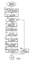
- FIG. 3 shows the interrupt handling routine that is executed by any of the CPUs when it is interrupted.
- the first action of the interrupt handling routine is temporarily to raise the internal priority level of the CPU to the maximum possible value. This ensures that the CPU will not be interrupted by a subsequent higher priority interrupt, before it has finished handling the current interrupt.
- the SEMAPHORE bit is then set, so as to ensure that no other CPU can access the control information at the same time. If the SEMAPHORE bit is already set, the CPU waits, since this means that another CPU is already accessing the control information.
- the CPU executes a CHANGE LEVEL subroutine. This updates the LEVEL table in the main store. It then scans the table to determine whether the current interrupt handler is still the CPU with the lowest priority level. If not, the lowest priority CPU is designated as the new interrupt handler and any inactive, pending, balanced interrupts are transferred to it from the old interrupt handler. Any active, pending, balanced interrupts are retained by the old interrupt handler, until they have been processed by it.
- the CHANGE LEVEL subroutine is described in more detail below with reference to Figure 4.
- the CPU now completes the interrupt processing. Details of the actions required to process the interrupt depend on the actual nature of the interrupt e.g. they may involve reading data from a disc file unit, or sending data to a printer. These actions form no part of the invention, and may be conventional, and so they will not be described in detail.
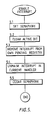
- this shows the CHANGE LEVEL subroutine in detail. As mentioned above, this is executed by a CPU when it changes level as a result of an interrupt. It is also executed if the CPU voluntarily changes level for any reason.
- the first action is to update the LEVEL table in main store, by setting the entry for this CPU to the priority level of the interrupt.
- the MASK register of the new handler is then combined, in a bit-by-bit OR function, with the bit-by-bit AND of TO-BE-BALANCED and the inverse of ACTIVE.
- the effect of this is to unmask the inactive, balanced interrupts in the new handler, so that they can now be received by the CPU. Any active interrupts remain masked, since they are not yet to be transferred.
- CHANGE LEVEL subroutine the program that calls it is responsible for setting the SEMAPHORE before the subroutine is called and for clearing it after the subroutine is executed.
- this shows the ENABLE INTERRUPT subroutine in detail.
- This subroutine is executed by a CPU whenever the CPU has processed an active interrupt to a stage such that it can now transfer responsibility for subsequent occurrences of that interrupt to the current interrupt handler.
- the first action is to set the SEMAPHORE bit.
- the internal priority level of the CPU is raised to the maximum possible value, so as to inhibit further interrupts.
- the old priority level of the CPU is saved.
Landscapes
- Engineering & Computer Science (AREA)
- Theoretical Computer Science (AREA)
- Computer Hardware Design (AREA)
- Physics & Mathematics (AREA)
- General Engineering & Computer Science (AREA)
- General Physics & Mathematics (AREA)
- Software Systems (AREA)
- Bus Control (AREA)
Applications Claiming Priority (2)
| Application Number | Priority Date | Filing Date | Title |
|---|---|---|---|
| GB888815042A GB8815042D0 (en) | 1988-06-24 | 1988-06-24 | Data processing apparatus |
| GB8815042 | 1988-06-24 |
Publications (2)
| Publication Number | Publication Date |
|---|---|
| EP0348076A1 true EP0348076A1 (de) | 1989-12-27 |
| EP0348076B1 EP0348076B1 (de) | 1992-12-02 |
Family
ID=10639280
Family Applications (1)
| Application Number | Title | Priority Date | Filing Date |
|---|---|---|---|
| EP89305794A Expired - Lifetime EP0348076B1 (de) | 1988-06-24 | 1989-06-08 | Einrichtung zur Datenverarbeitung |
Country Status (6)
| Country | Link |
|---|---|
| US (1) | US5099414A (de) |
| EP (1) | EP0348076B1 (de) |
| AU (1) | AU612269B2 (de) |
| DE (1) | DE68903693T2 (de) |
| GB (1) | GB8815042D0 (de) |
| ZA (1) | ZA894316B (de) |
Cited By (3)
| Publication number | Priority date | Publication date | Assignee | Title |
|---|---|---|---|---|
| EP0459714A2 (de) | 1990-06-01 | 1991-12-04 | AT&T Corp. | Unterbrechungsverarbeitungszuordnung in einem Mehrprozessorsystem |
| WO1993001553A1 (en) * | 1991-07-08 | 1993-01-21 | Seiko Epson Corporation | Microprocessor architecture capable of supporting multiple heterogeneous processors |
| EP0602858A1 (de) * | 1992-12-18 | 1994-06-22 | International Business Machines Corporation | Vorrichtung und Verfahren zur Unterbrechungsbedienung in einem Mehrrechnersystem |
Families Citing this family (26)
| Publication number | Priority date | Publication date | Assignee | Title |
|---|---|---|---|---|
| USRE38419E1 (en) | 1986-05-13 | 2004-02-10 | Ncr Corporation | Computer interface device |
| JP2855298B2 (ja) * | 1990-12-21 | 1999-02-10 | インテル・コーポレーション | 割込み要求の仲裁方法およびマルチプロセッサシステム |
| US5613128A (en) * | 1990-12-21 | 1997-03-18 | Intel Corporation | Programmable multi-processor interrupt controller system with a processor integrated local interrupt controller |
| JPH04246763A (ja) * | 1991-01-31 | 1992-09-02 | Nec Corp | マルチプロセッサ回路 |
| DE4211245B4 (de) * | 1991-04-05 | 2009-05-14 | Kabushiki Kaisha Toshiba, Kawasaki | Prozessorsystem in Parallelverarbeitungsbauart und Verfahren zu dessen Steuerung |
| AU2270892A (en) * | 1991-06-26 | 1993-01-25 | Ast Research, Inc. | Automatic distribution of interrupts controller for a multiple processor computer system |
| GB2257549B (en) * | 1991-07-06 | 1995-05-03 | Motorola Israel Ltd | Modular data/control equipment |
| US5590380A (en) * | 1992-04-22 | 1996-12-31 | Kabushiki Kaisha Toshiba | Multiprocessor system with processor arbitration and priority level setting by the selected processor |
| GB2298503B (en) * | 1993-12-16 | 1998-08-12 | Intel Corp | Multiple programmable interrupt controllers in a computer system |
| US5464435A (en) * | 1994-02-03 | 1995-11-07 | Medtronic, Inc. | Parallel processors in implantable medical device |
| US5613126A (en) * | 1994-05-31 | 1997-03-18 | Advanced Micro Devices, Inc. | Timer tick auto-chaining technique within a symmetrical multiprocessing system |
| US5802350A (en) * | 1996-01-18 | 1998-09-01 | International Business Machines Corporation | System and method for selecting an interrupt system based upon the operating system of a multiprocessor system |
| US5778236A (en) * | 1996-05-17 | 1998-07-07 | Advanced Micro Devices, Inc. | Multiprocessing interrupt controller on I/O bus |
| US5949994A (en) * | 1997-02-12 | 1999-09-07 | The Dow Chemical Company | Dedicated context-cycling computer with timed context |
| US6606676B1 (en) * | 1999-11-08 | 2003-08-12 | International Business Machines Corporation | Method and apparatus to distribute interrupts to multiple interrupt handlers in a distributed symmetric multiprocessor system |
| US6877057B2 (en) * | 2002-01-25 | 2005-04-05 | Dell Products L.P. | Information handling system with dynamic interrupt allocation apparatus and methodology |
| JP4017646B2 (ja) * | 2003-06-20 | 2007-12-05 | 富士通株式会社 | 割り込み制御方法、割り込み制御装置及び割り込み制御プログラム |
| US7222200B2 (en) * | 2004-10-14 | 2007-05-22 | Dell Products L.P. | Method for synchronizing processors in SMI following a memory hot plug event |
| US20060112208A1 (en) * | 2004-11-22 | 2006-05-25 | International Business Machines Corporation | Interrupt thresholding for SMT and multi processor systems |
| US7386642B2 (en) * | 2005-01-28 | 2008-06-10 | Sony Computer Entertainment Inc. | IO direct memory access system and method |
| US7680972B2 (en) * | 2005-02-04 | 2010-03-16 | Sony Computer Entertainment Inc. | Micro interrupt handler |
| JP2006216042A (ja) * | 2005-02-04 | 2006-08-17 | Sony Computer Entertainment Inc | 割り込み処理のためのシステムおよび方法 |
| US8463971B2 (en) * | 2005-08-22 | 2013-06-11 | Oracle America Inc. | Approach for distributing interrupts from high-interrupt load devices |
| US7581052B1 (en) * | 2005-08-22 | 2009-08-25 | Sun Microsystems, Inc. | Approach for distributing multiple interrupts among multiple processors |
| US7610425B2 (en) * | 2005-08-22 | 2009-10-27 | Sun Microsystems, Inc. | Approach for managing interrupt load distribution |
| CN117203616A (zh) * | 2021-05-31 | 2023-12-08 | 三星电子株式会社 | 电子设备及电子设备的传感器数据处理方法 |
Citations (2)
| Publication number | Priority date | Publication date | Assignee | Title |
|---|---|---|---|---|
| US3421150A (en) * | 1966-08-26 | 1969-01-07 | Sperry Rand Corp | Multiprocessor interrupt directory |
| EP0257348A2 (de) * | 1986-08-26 | 1988-03-02 | Bull HN Information Systems Inc. | Multiprozessor-Unterbrechungsumleitungsmechanismus |
Family Cites Families (6)
| Publication number | Priority date | Publication date | Assignee | Title |
|---|---|---|---|---|
| US3286236A (en) * | 1962-10-22 | 1966-11-15 | Burroughs Corp | Electronic digital computer with automatic interrupt control |
| US3665404A (en) * | 1970-04-09 | 1972-05-23 | Burroughs Corp | Multi-processor processing system having interprocessor interrupt apparatus |
| IT971304B (it) * | 1972-11-29 | 1974-04-30 | Honeywell Inf Systems | Sistema di accesso a priorita variabile dinamicamente |
| US4009470A (en) * | 1975-02-18 | 1977-02-22 | Sperry Rand Corporation | Pre-emptive, rotational priority system |
| US4271467A (en) * | 1979-01-02 | 1981-06-02 | Honeywell Information Systems Inc. | I/O Priority resolver |
| US4777587A (en) * | 1985-08-30 | 1988-10-11 | Advanced Micro Devices, Inc. | System for processing single-cycle branch instruction in a pipeline having relative, absolute, indirect and trap addresses |
-
1988
- 1988-06-24 GB GB888815042A patent/GB8815042D0/en active Pending
-
1989
- 1989-06-07 ZA ZA894316A patent/ZA894316B/xx unknown
- 1989-06-08 DE DE8989305794T patent/DE68903693T2/de not_active Expired - Fee Related
- 1989-06-08 EP EP89305794A patent/EP0348076B1/de not_active Expired - Lifetime
- 1989-06-12 US US07/364,881 patent/US5099414A/en not_active Expired - Lifetime
- 1989-06-23 AU AU36765/89A patent/AU612269B2/en not_active Ceased
Patent Citations (2)
| Publication number | Priority date | Publication date | Assignee | Title |
|---|---|---|---|---|
| US3421150A (en) * | 1966-08-26 | 1969-01-07 | Sperry Rand Corp | Multiprocessor interrupt directory |
| EP0257348A2 (de) * | 1986-08-26 | 1988-03-02 | Bull HN Information Systems Inc. | Multiprozessor-Unterbrechungsumleitungsmechanismus |
Non-Patent Citations (2)
| Title |
|---|
| NEW ELECTRONICS, vol. 18, no. 8, April 1985, page 28, London, GB; Q.A. RICE: "Hardware interrupt controller" * |
| OPERATING SYSTEMS REVIEW, vol. 21, no. 4, October 1987, pages 10-20, ACM, Washington, DC, US; B. BECK et al.: "VLSI assist for a multiprocessor" * |
Cited By (16)
| Publication number | Priority date | Publication date | Assignee | Title |
|---|---|---|---|---|
| EP0459714A2 (de) | 1990-06-01 | 1991-12-04 | AT&T Corp. | Unterbrechungsverarbeitungszuordnung in einem Mehrprozessorsystem |
| EP0459714A3 (en) * | 1990-06-01 | 1992-01-08 | American Telephone And Telegraph Company | Interrupt processing allocation in a multiprocessor system |
| JPH04232558A (ja) * | 1990-06-01 | 1992-08-20 | American Teleph & Telegr Co <Att> | マルチプロセッサシステム |
| US5179707A (en) * | 1990-06-01 | 1993-01-12 | At&T Bell Laboratories | Interrupt processing allocation in a multiprocessor system |
| US5604865A (en) * | 1991-07-08 | 1997-02-18 | Seiko Epson Corporation | Microprocessor architecture with a switch network for data transfer between cache, memory port, and IOU |
| US5440752A (en) * | 1991-07-08 | 1995-08-08 | Seiko Epson Corporation | Microprocessor architecture with a switch network for data transfer between cache, memory port, and IOU |
| WO1993001553A1 (en) * | 1991-07-08 | 1993-01-21 | Seiko Epson Corporation | Microprocessor architecture capable of supporting multiple heterogeneous processors |
| US5754800A (en) * | 1991-07-08 | 1998-05-19 | Seiko Epson Corporation | Multi processor system having dynamic priority based on row match of previously serviced address, number of times denied service and number of times serviced without interruption |
| US5941979A (en) * | 1991-07-08 | 1999-08-24 | Seiko Epson Corporation | Microprocessor architecture with a switch network and an arbitration unit for controlling access to memory ports |
| US6219763B1 (en) | 1991-07-08 | 2001-04-17 | Seiko Epson Corporation | System and method for adjusting priorities associated with multiple devices seeking access to a memory array unit |
| US6272579B1 (en) | 1991-07-08 | 2001-08-07 | Seiko Epson Corporation | Microprocessor architecture capable of supporting multiple heterogeneous processors |
| US6611908B2 (en) | 1991-07-08 | 2003-08-26 | Seiko Epson Corporation | Microprocessor architecture capable of supporting multiple heterogeneous processors |
| US6954844B2 (en) | 1991-07-08 | 2005-10-11 | Seiko Epson Corporation | Microprocessor architecture capable of supporting multiple heterogeneous processors |
| US7657712B2 (en) | 1991-07-08 | 2010-02-02 | Seiko Epson Corporation | Microprocessor architecture capable of supporting multiple heterogeneous processors |
| EP0602858A1 (de) * | 1992-12-18 | 1994-06-22 | International Business Machines Corporation | Vorrichtung und Verfahren zur Unterbrechungsbedienung in einem Mehrrechnersystem |
| US5379434A (en) * | 1992-12-18 | 1995-01-03 | International Business Machines Corporation | Apparatus and method for managing interrupts in a multiprocessor system |
Also Published As
| Publication number | Publication date |
|---|---|
| ZA894316B (en) | 1990-09-26 |
| DE68903693D1 (de) | 1993-01-14 |
| AU612269B2 (en) | 1991-07-04 |
| GB8815042D0 (en) | 1988-08-03 |
| DE68903693T2 (de) | 1993-06-17 |
| AU3676589A (en) | 1990-01-04 |
| US5099414A (en) | 1992-03-24 |
| EP0348076B1 (de) | 1992-12-02 |
Similar Documents
| Publication | Publication Date | Title |
|---|---|---|
| EP0348076B1 (de) | Einrichtung zur Datenverarbeitung | |
| EP0116591B1 (de) | Multiprozessorsystem zur behandlung von anrufen zwischen prozessoren | |
| US4959781A (en) | System for assigning interrupts to least busy processor that already loaded same class of interrupt routines | |
| US5193197A (en) | Apparatus and method for distributed dynamic priority arbitration for access to a shared resource | |
| EP1115060A2 (de) | Vorrichtung und Verfahren zur Durchführung von Hochgeschwindigkeitskontextumschaltung mit geringerer Systembelastung | |
| US5905898A (en) | Apparatus and method for storing interrupt source information in an interrupt controller based upon interrupt priority | |
| US5568643A (en) | Efficient interrupt control apparatus with a common interrupt control program and control method thereof | |
| US4615019A (en) | Data processing system with interrupt facilities | |
| KR930016879A (ko) | 공유메모리로의 배타적 액세스를 실행하는 멀티프로세서 시스템 | |
| US5249297A (en) | Methods and apparatus for carrying out transactions in a computer system | |
| US5850555A (en) | System and method for validating interrupts before presentation to a CPU | |
| KR0175983B1 (ko) | 데이타 처리 시스템 | |
| US5524211A (en) | System for employing select, pause, and identification registers to control communication among plural processors | |
| US5850558A (en) | System and method for referencing interrupt request information in a programmable interrupt controller | |
| US5894578A (en) | System and method for using random access memory in a programmable interrupt controller | |
| US5274825A (en) | Microprocessor vectored interrupts | |
| JP2594600B2 (ja) | シングルチップマイクロコンピュータ | |
| CN1133929C (zh) | 处理数据的负载共享系统及方法以及具有负载共享的通信系统 | |
| US6401144B1 (en) | Method and apparatus for managing data transfers between peripheral devices by encoding a start code in a line of data to initiate the data transfers | |
| US20020083257A1 (en) | Buffer page roll implementation for PCI-X block read transactions | |
| JP2731761B2 (ja) | ネットワーク制御装置 | |
| KR100294314B1 (ko) | 데이터처리시스템및방법과그런시스템과의통신시스템 | |
| US5933856A (en) | System and method for processing of memory data and communication system comprising such system | |
| EP0520835A2 (de) | Verriegelungsschema für Geräte in einem Rechnersystem | |
| EP0098170B1 (de) | Zugriffssteuerungsverarbeitungssystem in einem Computer-System |
Legal Events
| Date | Code | Title | Description |
|---|---|---|---|
| PUAI | Public reference made under article 153(3) epc to a published international application that has entered the european phase |
Free format text: ORIGINAL CODE: 0009012 |
|
| AK | Designated contracting states |
Kind code of ref document: A1 Designated state(s): DE FR GB IT NL |
|
| 17P | Request for examination filed |
Effective date: 19891116 |
|
| 17Q | First examination report despatched |
Effective date: 19920409 |
|
| ITF | It: translation for a ep patent filed | ||
| GRAA | (expected) grant |
Free format text: ORIGINAL CODE: 0009210 |
|
| AK | Designated contracting states |
Kind code of ref document: B1 Designated state(s): DE FR GB IT NL |
|
| REF | Corresponds to: |
Ref document number: 68903693 Country of ref document: DE Date of ref document: 19930114 |
|
| ET | Fr: translation filed | ||
| PLBE | No opposition filed within time limit |
Free format text: ORIGINAL CODE: 0009261 |
|
| STAA | Information on the status of an ep patent application or granted ep patent |
Free format text: STATUS: NO OPPOSITION FILED WITHIN TIME LIMIT |
|
| 26N | No opposition filed | ||
| PGFP | Annual fee paid to national office [announced via postgrant information from national office to epo] |
Ref country code: NL Payment date: 19990531 Year of fee payment: 11 |
|
| PGFP | Annual fee paid to national office [announced via postgrant information from national office to epo] |
Ref country code: DE Payment date: 20000524 Year of fee payment: 12 |
|
| PG25 | Lapsed in a contracting state [announced via postgrant information from national office to epo] |
Ref country code: NL Free format text: LAPSE BECAUSE OF NON-PAYMENT OF DUE FEES Effective date: 20010101 |
|
| NLV4 | Nl: lapsed or anulled due to non-payment of the annual fee |
Effective date: 20010101 |
|
| REG | Reference to a national code |
Ref country code: GB Ref legal event code: IF02 |
|
| PG25 | Lapsed in a contracting state [announced via postgrant information from national office to epo] |
Ref country code: DE Free format text: LAPSE BECAUSE OF NON-PAYMENT OF DUE FEES Effective date: 20020403 |
|
| PGFP | Annual fee paid to national office [announced via postgrant information from national office to epo] |
Ref country code: FR Payment date: 20020513 Year of fee payment: 14 |
|
| PG25 | Lapsed in a contracting state [announced via postgrant information from national office to epo] |
Ref country code: FR Free format text: LAPSE BECAUSE OF NON-PAYMENT OF DUE FEES Effective date: 20040227 |
|
| REG | Reference to a national code |
Ref country code: FR Ref legal event code: ST |
|
| PG25 | Lapsed in a contracting state [announced via postgrant information from national office to epo] |
Ref country code: IT Free format text: LAPSE BECAUSE OF NON-PAYMENT OF DUE FEES;WARNING: LAPSES OF ITALIAN PATENTS WITH EFFECTIVE DATE BEFORE 2007 MAY HAVE OCCURRED AT ANY TIME BEFORE 2007. THE CORRECT EFFECTIVE DATE MAY BE DIFFERENT FROM THE ONE RECORDED. Effective date: 20050608 |
|
| PGFP | Annual fee paid to national office [announced via postgrant information from national office to epo] |
Ref country code: GB Payment date: 20060516 Year of fee payment: 18 |
|
| GBPC | Gb: european patent ceased through non-payment of renewal fee |
Effective date: 20070608 |
|
| PG25 | Lapsed in a contracting state [announced via postgrant information from national office to epo] |
Ref country code: GB Free format text: LAPSE BECAUSE OF NON-PAYMENT OF DUE FEES Effective date: 20070608 |