EP0347993A2 - Mikrowellen-Oszillatoreinrichtungen - Google Patents
Mikrowellen-Oszillatoreinrichtungen Download PDFInfo
- Publication number
- EP0347993A2 EP0347993A2 EP19890201593 EP89201593A EP0347993A2 EP 0347993 A2 EP0347993 A2 EP 0347993A2 EP 19890201593 EP19890201593 EP 19890201593 EP 89201593 A EP89201593 A EP 89201593A EP 0347993 A2 EP0347993 A2 EP 0347993A2
- Authority
- EP
- European Patent Office
- Prior art keywords
- wire
- terminal
- connection
- bonding area
- length
- Prior art date
- Legal status (The legal status is an assumption and is not a legal conclusion. Google has not performed a legal analysis and makes no representation as to the accuracy of the status listed.)
- Granted
Links
Images
Classifications
-
- H—ELECTRICITY
- H03—ELECTRONIC CIRCUITRY
- H03B—GENERATION OF OSCILLATIONS, DIRECTLY OR BY FREQUENCY-CHANGING, BY CIRCUITS EMPLOYING ACTIVE ELEMENTS WHICH OPERATE IN A NON-SWITCHING MANNER; GENERATION OF NOISE BY SUCH CIRCUITS
- H03B5/00—Generation of oscillations using amplifier with regenerative feedback from output to input
- H03B5/18—Generation of oscillations using amplifier with regenerative feedback from output to input with frequency-determining element comprising distributed inductance and capacitance
- H03B5/1841—Generation of oscillations using amplifier with regenerative feedback from output to input with frequency-determining element comprising distributed inductance and capacitance the frequency-determining element being a strip line resonator
- H03B5/1847—Generation of oscillations using amplifier with regenerative feedback from output to input with frequency-determining element comprising distributed inductance and capacitance the frequency-determining element being a strip line resonator the active element in the amplifier being a semiconductor device
- H03B5/1852—Generation of oscillations using amplifier with regenerative feedback from output to input with frequency-determining element comprising distributed inductance and capacitance the frequency-determining element being a strip line resonator the active element in the amplifier being a semiconductor device the semiconductor device being a field-effect device
-
- H—ELECTRICITY
- H03—ELECTRONIC CIRCUITRY
- H03B—GENERATION OF OSCILLATIONS, DIRECTLY OR BY FREQUENCY-CHANGING, BY CIRCUITS EMPLOYING ACTIVE ELEMENTS WHICH OPERATE IN A NON-SWITCHING MANNER; GENERATION OF NOISE BY SUCH CIRCUITS
- H03B5/00—Generation of oscillations using amplifier with regenerative feedback from output to input
- H03B5/18—Generation of oscillations using amplifier with regenerative feedback from output to input with frequency-determining element comprising distributed inductance and capacitance
-
- H—ELECTRICITY
- H03—ELECTRONIC CIRCUITRY
- H03B—GENERATION OF OSCILLATIONS, DIRECTLY OR BY FREQUENCY-CHANGING, BY CIRCUITS EMPLOYING ACTIVE ELEMENTS WHICH OPERATE IN A NON-SWITCHING MANNER; GENERATION OF NOISE BY SUCH CIRCUITS
- H03B9/00—Generation of oscillations using transit-time effects
- H03B9/12—Generation of oscillations using transit-time effects using solid state devices, e.g. Gunn-effect devices
-
- H—ELECTRICITY
- H03—ELECTRONIC CIRCUITRY
- H03B—GENERATION OF OSCILLATIONS, DIRECTLY OR BY FREQUENCY-CHANGING, BY CIRCUITS EMPLOYING ACTIVE ELEMENTS WHICH OPERATE IN A NON-SWITCHING MANNER; GENERATION OF NOISE BY SUCH CIRCUITS
- H03B2200/00—Indexing scheme relating to details of oscillators covered by H03B
- H03B2200/003—Circuit elements of oscillators
- H03B2200/0032—Circuit elements of oscillators including a device with a Schottky junction
-
- H10W72/07554—
-
- H10W72/534—
-
- H10W72/5453—
-
- H10W72/547—
-
- H10W72/5473—
-
- H10W72/5522—
-
- H10W72/59—
-
- H10W72/926—
-
- H10W72/936—
-
- H10W72/952—
-
- H10W90/00—
-
- H10W90/753—
-
- H10W90/756—
Definitions
- This invention relates to microwave oscillator devices comprising a transistor body, particularly but not exclusively a Schottky-gate field-effect transistor (a so-called "MESFET”) of gallium arsenide, with electrical connections including lengths of wire which form inductors in a feedback path. More particularly, the invention provides a two-terminal device of this form as a replacement for a Gunn diode.
- a Schottky-gate field-effect transistor a so-called "MESFET”
- the invention provides a two-terminal device of this form as a replacement for a Gunn diode.
- an active semiconductor device requires a negative-resistance characteristic.
- a negative resistance is inherent in devices such as Gunn diodes (also called transferred electron devices), IMPATT diodes and tunnel diodes and is obtained by simply applying a dc bias to the two electrodes of the device.
- the negative-resistance state has to be simulated by suitable feedback between the electrodes of the transistor, and inductive connections are used for this purpose.
- the resulting arrangement may be a three-terminal or two-terminal device.
- European patent application EP-A-0 156 708 discloses a microwave oscillator device comprising a transistor body (a FET in this case) having first and second main electrodes (source and drain) and a control electrode (gate); a microwave device envelope comprising an electrically insulating surround within which the transistor body is mounted on a base of the envelope; and electrical connections between the electrodes of the transistor and electrical terminals of the device.
- a first terminal is provided by the base, and a second terminal is carried by the surround.
- the connection to the second main electrode (source) comprises in series at least first and second lengths of wire.
- the connection to the control electrode comprises a third length of wire. At least the second and third lengths of wire form inductors in a feedback path between the control electrode and the second main electrode.
- the oscillator of EP-A-0 156 708 includes a tuning circuit comprising a varicap diode connected to the source electrode of the FET by the first length of wire. This first length is kept as short as possible in this known device so as to have no significant inductance.
- the device envelope is that of a microwave transistor and has a third terminal which is also carried by the insulating surround.
- the base is of metal and forms an earth terminal of the device.
- the FET body and varicap body are mounted to a first capacitor on the base.
- a second capacitor and a resistor are also mounted on the base, beside the first capacitor.
- the top of the first capacitor is connected to the third terminal by one connection wire, and the drain of the FET is connected to the second terminal by another connection wire.
- the source electrode is connected by the very short first wire to the top of the varicap body, and the second wire extends from the top of the varicap body to the top of the second capacitor which effectively couples this second wire inductor to earth at microwave frequencies.
- the gate of the FET is connected directly to the earth terminal by the inductive third wire bonded to the metal base. This gate connection wire is longer than the first and second wire connections for the source of the FET and so provides a larger inductance in the gate connection.
- a further wire extends from the top of the second capacitor to the top of the resistor to form a bias circuit connected to earth.
- the present invention is based on a recognition by the present inventor that a microwave oscillator device comprising a transistor body can be constructed as a replacement both electrically and mechanically for a Gunn diode by adopting within a microwave diode envelope a different and inverted connection arrangement in which the first main electrode is connected to the base terminal(instead of to the second terminal) and in which wire connections for both the control electrode and the second main electrode are isolated from the base and connected together electrically to the second terminal at the top of the surround so as to provide inductive feedback by way of a dc coupling in which the connection for the second main electrode comprises in series more than one upwardly-extending inductive length of wire (utilizing one or more bonding areas) so as to have a total inductance which is high compared with the inductance of the wire connection for the gate.
- Such an inverted connection arrangement permits long inductive lengths of wire to be compressed into a small space, and may be made readily compatible with the small space and the bonding areas available inside an envelope of conventional two-terminal outline for a Gunn diode.
- Such a device may perform as an electrical equivalent to a Gunn diode (having the same impedance as seen at the terminals) but with a higher efficiency in its dc to microwave conversion than a Gunn diode.
- a microwave oscillator device comprising a transistor body having first and second main electrodes and a control electrode, a microwave device envelope comprising an electrically insulating surround within which the transistor body is mounted on a base of the envelope, and electrical connections between the electrodes of the transistor body and electrical terminals of the device, of which a first terminal is provided by the base and of which a second terminal is carried by the surround, the connection to the second main electrode comprising in series at least first and second lengths of wire, the connection to the control electrode comprising a third length of wire, the second and third lengths of wire forming inductors in a feedback path between the control electrode and the second main electrode, which device is characterised in that the envelope comprises an upper bonding area which is present adjacent the top of the surround and which is electrically connected to the second terminal, and a lower bonding area which is present adjacent the base and which is electrically insulated from the first terminal, in that the first main electrode is connected to the first terminal, in that the first length of wire extends
- the first length of wire may be increased by arching the wire and/or more than one separate bonding area may be provided at the bottom of the available space for the inclusion of further wires in the series connection.
- the arrangement may be such that the lower bonding area comprises first and second separate areas which are present beside the transistor body, and that the connection to the second main electrode comprises the first length of wire extending from the electrode to the first area, the second length of wire extending from the second area to the upper bonding area, and a fourth length of wire extending from the first area to the second area.
- the fourth length of wire extends to a height which is above half (or even above three quarters of) the height of the upper bonding area above the base, thereby increasing the length (and hence the inductance) of the fourth length of wire.
- the first length of wire may extend to about the same height, thereby increasing the inductance of the first length.
- the transistor body may comprise a bipolar transistor having a collector as the first main electrode, an emitter as the second main electrode, and a base as the control electrode.
- a bipolar transistor having a collector as the first main electrode, an emitter as the second main electrode, and a base as the control electrode.
- a unipolar device such as a field-effect transistor, especially a FET formed in gallium arsenide or another III-V compound semiconductor material(s) having a high electron mobility.
- the transistor body comprises a Schottky-gate FET having drain and source main electrodes and a gate control electrode.
- the transistor body often comprises a substrate of semi-insulating material, and so a compatible manfacturing process can be adopted in which the lower bonding area provided in accordance with the invention comprises metallization on a substrate of the semi-insulating material having the same thickness as the substrate of the transistor body.
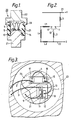
- the microwave oscillator device of Figure 1 comprises a transistor body 10 having first and second main electrodes 11 and 12 respectively ( Figure 3) and a control electrode 13.
- a microwave device envelope 20 comprises an electrically insulating surround 25 within which the transistor body 10 is mounted on a base 21 of the envelope. Electrical connections 1 to 5 are present between the electrodes of the transistor body 10 and electrical terminals 21 and 22 of the device. Of these a first terminal 21 is provided by the base, and a second terminal 22 is carried by the surround 25.
- the connection to the second main electrode 12 comprises in series at least first and second lengths of wire 1 and 2 respectively.
- the connection to the control electrode 13 comprises a third length of wire 3.
- the second and third lengths of wire 2 and 3 form inductors L2 and L3 (see Figure 2) in a feedback path between the control electrode 13 and the second main electrode 12.
- the envelope 20 comprises an upper bonding area 23 which is present adjacent the top of the surround 25 and which is electrically connected to the second terminal 22, and a lower bonding area 15,16,17 which is present adjacent the base 21 and which is electrically insulated from the first terminal 21.
- the first main electrode 11 is connected to the first terminal 21.
- the first length 1 of wire extends to the lower bonding area 15,16,17.
- the second length 2 of wire extends from the lower bonding area 15,16,17 to the upper bonding area 23.
- the third length of wire 3 extends to the upper bonding area 23.
- connection of both the second and third lengths 2 and 3 to the second terminal 22 provides a dc coupling via the inductive feedback path (L1,L2,L3, and possibly L4) in which the inductance L1 and L2 (and possibly L4) of the connection 1,2 (and possibly 4) between the second main electrode 12 and the second terminal 22 is higher than the inductance L3 of the connection 3 between the control electrode 13 and the second terminal 22.
- the device of Figure 1 is an electrical and mechanical replacement for a Gunn diode.
- the envelope 20 diagrammatically illustrated in Figure 1 can be of the same outline as one of the conventionally used Gunn diode envelopes such as, for example, the international standard SOD 31 type having a double-ended cylindrical geometry.
- the envelope base 21 provides the terminal to which the dc bias voltage (+V in Figure 2) is applied at one end of the device.
- the envelope 20 comprises a cover 22 which is mounted on top of the insulating cylindrical surround 25 and which provides the earth terminal. Both the second and third lengths of wire 2 and 3 are connected to this second terminal 22 (and not to the base) which is the opposite situation to that of the oscillator in EP-A-0 156 708.
- the envelope 20 may have the same structure as a conventional Gunn diode envelope.
- the base 21 may be of metal (for example gold-plated copper) forming the first terminal at one end of the insulating surround 25;
- the transistor body 10 may be mounted on a plinth of this base 21;
- the surround 25 may be of ceramic (for example alumina) and may have a metal ring 23 (for example "Kovar" Trade Mark) forming a flange at the top of the surround 25;
- the connections 1 to 5 may be, for example, gold wires; the wires 2 and 3 can be bonded in known manner to the ring 23, and the cover terminal 22 of metal (for example gold-plated copper) may be welded to the ring 23.
- the oscillator device can have an electrical performance resembling that of a Gunn diode with the same microwave impedances seen at its terminals 21 and 22 but with a high efficiency in dc to microwave conversion (typically 10 to 30 percent, as compared with 1 to 3 percent for a Gunn diode).
- the appropriate circuit diagram with inductive feedback between electrodes 13 and 12 is shown in Figure 2.
- the transistor body 10 comprises a Schottky-gate field-effect transistor, for example a gallium arsenide MESFET, having drain electrode 11, source electrode 12 and gate electrode 13. These electrodes 11 to 13 may comprise gold, for example.
- the transistor body 10 comprises the active transistor structure formed in and on an epitaxial layer of n -type semiconducting gallium arsenide on a substrate of semi-insulating material, for example chromium-doped gallium arsenide.
- the body 10 may be attached to the base 21 by an intermediate layer 24 of, for example, an insulating epoxy or other adhesive.
- the bonding area 15,16,17 may comprise metallization 16,17 (for example gold) on a substrate 15 of the same semi-insulating material and same thickness as the substrate of the transistor body.
- This substrate 15 may be a lateral extension of the substrate of the transistor body 10, or it may be a separate substrate (as illustrated in Figures 1 and 3) separately attached to the base 21 by an intermediate adhesive layer 24.
- the source connection comprises only the first and second lengths of wire 1 and 2 extending to and from one lower bonding area, the length 1 being increased by arching upwards in the available space below the cover 22 (as illustrated in Figure 1) so as to form a significant inductance L1 for the first wire 1.
- the inductance L1 may even be chosen to be larger than the inductance L3 of the gate connection 3, so that the total inductance (L1+L2) of the source connection 1,2 in the feedback path is more than two times larger than the inductance L3 of the gate connection. This is the opposite situation to that of the oscillator device of EP-A-0 156 708.
- the lower bonding area 15,16,17 comprises separate first and second metallization areas 16 and 17 respectively, beside the transistor body 10.
- the connection to the second main electrode 12 in this case now comprises the first length of wire 1 extending from the electrode 12 to the first bonding area 16, the second length of wire 2 extending from the second bonding area 17 to the top of the surround 25, and a fourth length of wire 4 extending from the first bonding area 16 to the second bonding area 17.
- these separate metallization areas 16 and 17 are provided on the same substrate 15, but they may be provided on separate substrates.
- the lengths 1,4 and 2 may be formed by a single wire stitch-bonded so as to hop between the areas 12,16,17 and 23.
- the arched wires 1 and 4 may extend to substantially the same height in the envelope space and this facilitates their provision in the wire bonding operation, particularly with stitch-bonding.
- the wires 1 and 4 may be arched to a height above the base 21 in excess of half (and even three quarters) of the height of the upper bonding area 23 above the base 21.
- the maximum height to which the wires 1 and 4 can be arched may be determined by the reliability and reproducibility of the wire bonding operation which are achievable with the particular bonding machine used and the particular form of wire used, as well as the shape of the envelope space. In the particular example illustrated in Figure 1, there is a recess in the underside of the cover 22 which provides more space so that the wire 1 (and wire 4) may even be arched to a height near or above the top of the upper bonding area 23.
- the total inductance L1,L2 (and possibly L4) of the source connection 1,2 (and possibly 4) may be about 3nH, and the inductance L3 of the gate connection 3 may be about 1nH, whereas the inductance L5 in the drain connection 5 is very much less, for example about 0.5nH.
- an inductance of about 1nH per mm of the wire is obtained.
- the height inside the envelope 20, between the plinth of the base 21 and the top of the bonding ring 23 may be about 0.75mm, and the bodies 10 and 15 may each be about 0.1mm high.
- the wires 2 and 3 may each have a length of about 1mm and hence an inductance of about 1nH, and the remaining inductance (about 2nH) required for the source connection may be obtained by using two lengths 1 and 4 of wire which may be arched to a lower height in the envelope space.
- connection arrangement results in a broad-band oscillator which oscillates at a frequency determined by the dimensions of a resonant waveguide cavity in which the device is mounted in operation.
- connection arrangement of the FET of EP-A-0 156 708 (having varactor tuning in the source connection and a higher inductance in the gate connection than in the source connection) results in an oscillator whose frequency is determined by the inductance (wire length) in the source connection.
- wires 1 to 5 may be employed with other shaped cross-sections if desired, for example a rectangular cross-section for at least some of the wires 1 to 5 so that these wires may have the nature of straps.
- the upper bonding area 23 may be provided in some other manner, for example as a metallization layer on a surface of the insulating surround 25 on the top of the surround 25 or for example on a ledge near the top of the surround 25.
- the lower bonding area 15,16,17 for the source connection wires may be provided on a different surface from the top of the plinth on which the transistor body 10 is mounted.
- the lower bonding area may be metallization provided on a low ledge of the insulating surround 25 adjacent the base 21, or it may be mounted on a lower ledge of the base 21 while still being electrically insulated from the first terminal.
- the source connection wires in the oscillator of EP-A-0 156 708 were coupled electrically to the base terminal by capacitors
- the source connection wires 1,2,4 in the oscillator of the present invention are insulated from the base terminal 21 (both at dc and microwave frequencies) and are dc coupled to the upper earth terminal 22.
- the cover 22 and base 21 are formed wholly of metal in a conventional microwave device envelope, other constructions could be used in which part of the cover 22 and/or base 21 is electrically insulating whereas another part is electrically conductive and forms the terminal connections of the device.
- the transistor body 10 in an oscillator in accordance with the present invention may comprise a bipolar transistor.
- the transistor may have its emitter and base electrodes 12 and 13 respectively at the top surface of the body and its collector electrode 11 at the bottom surface.
- Such a bipolar transistor body may be mounted on a metallised surface of the metal base 21 so as to form a direct connection between the collector electrode 11 and the device terminal 21 without requiring a wire 5.
- the dc path between the source and gate electrodes 12 and 13 may include a resistor (for example between wires 2 and 4) to set a desired bias condition for the transistor.
- a decoupling capacitor is coupled in parallel with the resistor.
Landscapes
- Inductance-Capacitance Distribution Constants And Capacitance-Resistance Oscillators (AREA)
- Wire Bonding (AREA)
- Junction Field-Effect Transistors (AREA)
Applications Claiming Priority (2)
| Application Number | Priority Date | Filing Date | Title |
|---|---|---|---|
| GB8814889A GB2220113B (en) | 1988-06-22 | 1988-06-22 | Microwave oscillator devices |
| GB8814889 | 1988-06-22 |
Publications (3)
| Publication Number | Publication Date |
|---|---|
| EP0347993A2 true EP0347993A2 (de) | 1989-12-27 |
| EP0347993A3 EP0347993A3 (de) | 1991-03-27 |
| EP0347993B1 EP0347993B1 (de) | 1994-06-08 |
Family
ID=10639174
Family Applications (1)
| Application Number | Title | Priority Date | Filing Date |
|---|---|---|---|
| EP89201593A Expired - Lifetime EP0347993B1 (de) | 1988-06-22 | 1989-06-19 | Mikrowellen-Oszillatoreinrichtungen |
Country Status (5)
| Country | Link |
|---|---|
| US (1) | US4947138A (de) |
| EP (1) | EP0347993B1 (de) |
| JP (1) | JPH0244904A (de) |
| DE (1) | DE68915862T2 (de) |
| GB (1) | GB2220113B (de) |
Cited By (2)
| Publication number | Priority date | Publication date | Assignee | Title |
|---|---|---|---|---|
| EP0656683A1 (de) * | 1993-12-03 | 1995-06-07 | Deutsche Thomson-Brandt Gmbh | Anordnung zur Verringerung von Störungen bei Schwingkreisen in integrierten Schaltungen |
| WO2002041487A1 (de) * | 2000-11-17 | 2002-05-23 | Infineon Technologies Ag | Oszillatorschaltung |
Families Citing this family (2)
| Publication number | Priority date | Publication date | Assignee | Title |
|---|---|---|---|---|
| JP3850325B2 (ja) * | 2002-03-27 | 2006-11-29 | 株式会社東芝 | マイクロ波集積回路 |
| DE102006007380B4 (de) * | 2005-12-07 | 2017-12-14 | René Zimmer | Hochfrequenzgenerator, Hochfrequenzsender und deren Verwendung, insbesondere zur Erzeugung von UWB-Signalen |
Family Cites Families (3)
| Publication number | Priority date | Publication date | Assignee | Title |
|---|---|---|---|---|
| FR2561048B1 (fr) * | 1984-03-09 | 1986-09-19 | Thomson Csf | Oscillateur hyperfrequences a transistor, commande par capacite variable |
| JPS6122656A (ja) * | 1984-07-10 | 1986-01-31 | Nec Corp | 発振用トランジスタ素子 |
| US4768079A (en) * | 1984-08-07 | 1988-08-30 | M/A Com, Inc. | Field effect transistor device |
-
1988
- 1988-06-22 GB GB8814889A patent/GB2220113B/en not_active Expired - Lifetime
-
1989
- 1989-06-05 US US07/361,526 patent/US4947138A/en not_active Expired - Fee Related
- 1989-06-19 DE DE68915862T patent/DE68915862T2/de not_active Expired - Fee Related
- 1989-06-19 EP EP89201593A patent/EP0347993B1/de not_active Expired - Lifetime
- 1989-06-20 JP JP1155922A patent/JPH0244904A/ja active Pending
Cited By (3)
| Publication number | Priority date | Publication date | Assignee | Title |
|---|---|---|---|---|
| EP0656683A1 (de) * | 1993-12-03 | 1995-06-07 | Deutsche Thomson-Brandt Gmbh | Anordnung zur Verringerung von Störungen bei Schwingkreisen in integrierten Schaltungen |
| WO2002041487A1 (de) * | 2000-11-17 | 2002-05-23 | Infineon Technologies Ag | Oszillatorschaltung |
| US6806785B2 (en) | 2000-11-17 | 2004-10-19 | Infineon Technologies Ag | Oscillator circuit using bonding wires for inductors and having a resonance transformation circuit |
Also Published As
| Publication number | Publication date |
|---|---|
| GB2220113A (en) | 1989-12-28 |
| JPH0244904A (ja) | 1990-02-14 |
| EP0347993B1 (de) | 1994-06-08 |
| GB2220113B (en) | 1992-02-12 |
| DE68915862T2 (de) | 1994-12-22 |
| EP0347993A3 (de) | 1991-03-27 |
| US4947138A (en) | 1990-08-07 |
| GB8814889D0 (en) | 1988-07-27 |
| DE68915862D1 (de) | 1994-07-14 |
Similar Documents
| Publication | Publication Date | Title |
|---|---|---|
| CN1643685A (zh) | 功率放大器器件 | |
| JP2800566B2 (ja) | 電界効果トランジスタおよび高周波信号発振器および周波数変換回路 | |
| US4266239A (en) | Semiconductor device having improved high frequency characteristics | |
| EP0018091B1 (de) | Halbleitervorrichtung mit mehreren Halbleiter-Chipportionen | |
| US4458215A (en) | Monolithic voltage controlled oscillator | |
| EP0379258A2 (de) | Abstimmbare Hohlleiter-Oszillatoren | |
| JPH10223674A (ja) | 半導体の入出力接続構造 | |
| US4947138A (en) | Microwave oscillator devices | |
| US8912647B2 (en) | Semiconductor device for smoothing the voltage of the end face of a drain of a high frequency semiconductor chip | |
| US5126827A (en) | Semiconductor chip header having particular surface metallization | |
| US4647867A (en) | High-frequency, high-gain, push-pull amplifier circuit | |
| EP0174457B1 (de) | Transistorvorrichtungen für Mikrowellen-Schwingelemente | |
| US5406114A (en) | Bipolar high-frequency transistor | |
| JPS60206305A (ja) | 可変コンデンサ制御形トランジスタ超高周波発振器 | |
| JPS6017931Y2 (ja) | 超高周波トランジスタ発振器 | |
| JPH07120906B2 (ja) | マイクロ波ミリ波高出力トランジスタ | |
| US20240145413A1 (en) | Semiconductor device | |
| JPH0697203A (ja) | 半導体装置 | |
| JPS63280463A (ja) | 半導体装置 | |
| JPS6364081B2 (de) | ||
| JP4164013B2 (ja) | 半導体装置 | |
| JPS6318705A (ja) | Vco用電界効果トランジスタ | |
| JPH07142626A (ja) | 半導体装置 | |
| JPS6032749Y2 (ja) | チップ形静電容量素子 | |
| JPH0513539B2 (de) |
Legal Events
| Date | Code | Title | Description |
|---|---|---|---|
| PUAI | Public reference made under article 153(3) epc to a published international application that has entered the european phase |
Free format text: ORIGINAL CODE: 0009012 |
|
| AK | Designated contracting states |
Kind code of ref document: A2 Designated state(s): DE FR GB IT NL |
|
| PUAL | Search report despatched |
Free format text: ORIGINAL CODE: 0009013 |
|
| AK | Designated contracting states |
Kind code of ref document: A3 Designated state(s): DE FR GB IT NL |
|
| 17P | Request for examination filed |
Effective date: 19910923 |
|
| RAP3 | Party data changed (applicant data changed or rights of an application transferred) |
Owner name: N.V. PHILIPS' GLOEILAMPENFABRIEKEN Owner name: PHILIPS ELECTRONICS UK LIMITED |
|
| 17Q | First examination report despatched |
Effective date: 19930708 |
|
| GRAA | (expected) grant |
Free format text: ORIGINAL CODE: 0009210 |
|
| AK | Designated contracting states |
Kind code of ref document: B1 Designated state(s): DE FR GB IT NL |
|
| PG25 | Lapsed in a contracting state [announced via postgrant information from national office to epo] |
Ref country code: IT Free format text: LAPSE BECAUSE OF FAILURE TO SUBMIT A TRANSLATION OF THE DESCRIPTION OR TO PAY THE FEE WITHIN THE PRESCRIBED TIME-LIMIT;WARNING: LAPSES OF ITALIAN PATENTS WITH EFFECTIVE DATE BEFORE 2007 MAY HAVE OCCURRED AT ANY TIME BEFORE 2007. THE CORRECT EFFECTIVE DATE MAY BE DIFFERENT FROM THE ONE RECORDED. Effective date: 19940608 Ref country code: NL Effective date: 19940608 |
|
| REF | Corresponds to: |
Ref document number: 68915862 Country of ref document: DE Date of ref document: 19940714 |
|
| ET | Fr: translation filed | ||
| NLV1 | Nl: lapsed or annulled due to failure to fulfill the requirements of art. 29p and 29m of the patents act | ||
| PLBE | No opposition filed within time limit |
Free format text: ORIGINAL CODE: 0009261 |
|
| STAA | Information on the status of an ep patent application or granted ep patent |
Free format text: STATUS: NO OPPOSITION FILED WITHIN TIME LIMIT |
|
| 26N | No opposition filed | ||
| PGFP | Annual fee paid to national office [announced via postgrant information from national office to epo] |
Ref country code: GB Payment date: 19950531 Year of fee payment: 7 |
|
| REG | Reference to a national code |
Ref country code: FR Ref legal event code: CD |
|
| PGFP | Annual fee paid to national office [announced via postgrant information from national office to epo] |
Ref country code: FR Payment date: 19950628 Year of fee payment: 7 |
|
| PGFP | Annual fee paid to national office [announced via postgrant information from national office to epo] |
Ref country code: DE Payment date: 19950822 Year of fee payment: 7 |
|
| PG25 | Lapsed in a contracting state [announced via postgrant information from national office to epo] |
Ref country code: GB Effective date: 19960619 |
|
| GBPC | Gb: european patent ceased through non-payment of renewal fee |
Effective date: 19960619 |
|
| PG25 | Lapsed in a contracting state [announced via postgrant information from national office to epo] |
Ref country code: FR Effective date: 19970228 |
|
| PG25 | Lapsed in a contracting state [announced via postgrant information from national office to epo] |
Ref country code: DE Effective date: 19970301 |
|
| REG | Reference to a national code |
Ref country code: FR Ref legal event code: ST |