EP0347983A2 - Circuit électronique de commande de délai - Google Patents
Circuit électronique de commande de délai Download PDFInfo
- Publication number
- EP0347983A2 EP0347983A2 EP89201549A EP89201549A EP0347983A2 EP 0347983 A2 EP0347983 A2 EP 0347983A2 EP 89201549 A EP89201549 A EP 89201549A EP 89201549 A EP89201549 A EP 89201549A EP 0347983 A2 EP0347983 A2 EP 0347983A2
- Authority
- EP
- European Patent Office
- Prior art keywords
- input
- signal
- pulse signal
- pulse
- delay
- Prior art date
- Legal status (The legal status is an assumption and is not a legal conclusion. Google has not performed a legal analysis and makes no representation as to the accuracy of the status listed.)
- Withdrawn
Links
Images


Classifications
-
- H—ELECTRICITY
- H03—ELECTRONIC CIRCUITRY
- H03K—PULSE TECHNIQUE
- H03K5/00—Manipulating of pulses not covered by one of the other main groups of this subclass
- H03K5/13—Arrangements having a single output and transforming input signals into pulses delivered at desired time intervals
- H03K5/133—Arrangements having a single output and transforming input signals into pulses delivered at desired time intervals using a chain of active delay devices
-
- H—ELECTRICITY
- H03—ELECTRONIC CIRCUITRY
- H03K—PULSE TECHNIQUE
- H03K5/00—Manipulating of pulses not covered by one of the other main groups of this subclass
- H03K2005/00013—Delay, i.e. output pulse is delayed after input pulse and pulse length of output pulse is dependent on pulse length of input pulse
- H03K2005/00019—Variable delay
- H03K2005/00026—Variable delay controlled by an analog electrical signal, e.g. obtained after conversion by a D/A converter
- H03K2005/00052—Variable delay controlled by an analog electrical signal, e.g. obtained after conversion by a D/A converter by mixing the outputs of fixed delayed signals with each other or with the input signal
-
- H—ELECTRICITY
- H03—ELECTRONIC CIRCUITRY
- H03K—PULSE TECHNIQUE
- H03K5/00—Manipulating of pulses not covered by one of the other main groups of this subclass
- H03K2005/00013—Delay, i.e. output pulse is delayed after input pulse and pulse length of output pulse is dependent on pulse length of input pulse
- H03K2005/0015—Layout of the delay element
- H03K2005/00163—Layout of the delay element using bipolar transistors
- H03K2005/00176—Layout of the delay element using bipolar transistors using differential stages
-
- H—ELECTRICITY
- H03—ELECTRONIC CIRCUITRY
- H03K—PULSE TECHNIQUE
- H03K5/00—Manipulating of pulses not covered by one of the other main groups of this subclass
- H03K2005/00013—Delay, i.e. output pulse is delayed after input pulse and pulse length of output pulse is dependent on pulse length of input pulse
- H03K2005/0015—Layout of the delay element
- H03K2005/00163—Layout of the delay element using bipolar transistors
- H03K2005/00182—Layout of the delay element using bipolar transistors using constant current sources
-
- H—ELECTRICITY
- H03—ELECTRONIC CIRCUITRY
- H03K—PULSE TECHNIQUE
- H03K5/00—Manipulating of pulses not covered by one of the other main groups of this subclass
- H03K2005/00013—Delay, i.e. output pulse is delayed after input pulse and pulse length of output pulse is dependent on pulse length of input pulse
- H03K2005/0015—Layout of the delay element
- H03K2005/00228—Layout of the delay element having complementary input and output signals
Definitions
- the present invention relates to digital delay circuits, and more particularly to an electronic delay control circuit that delays an input pulse without changing the pulse width.
- delay may be achieved by inputting a pulse signal to a shift register having a plurality of taps, and then selecting the appropriate tap for the desired delay.
- the delay is an integer multiple of the clock signal that clocks the shift register, and does not provide for adjustment within the range of values less than one clock cycle.
- analog type delay lines with variable components can be used to provide a constantly variable delay time, but such circuits tend to alter the pulse width of the resulting delayed pulse signal.
- Another technique is to convert the pulse signal into a ramp signal that is input to a comparator for comparison with a variable reference voltage. Again this provides a constantly variable delay time, but at the expense of altering the width of the pulse signal.
- What is desired is an electronic delay control circuit that provides a constantly variable delay while maintaining a desired pulse width, i.e., that delays both the leading and trailing edge of the input pulse signal equally.
- the present invention provides an electronic delay control circuit that variably delays equally both the leading and trailing edges of an input pulse signal.
- a pulse signal to be delayed is one input to a first comparator and a reference signal is the other input.
- the pulse signal together with the reference signal also is input to a second and third comparator at opposite inputs.
- the outputs of the second and third comparators are input to a pulse shaping network and added to the output of the first comparator to change the slope of the edges of the pulse output of the first comparator.
- a current steering circuit in response to a delay control signal steers a constant current source between the second and third comparators to vary the amplitude of the outputs of the second and third comparators, and thus the edge slopes of the output pulse signal.
- the output pulse signal is buffered and output as a delayed pulse signal.
- a pulse signal is input to a first comparator 12 together with a reference signal REF1 to produce a corresponding pulse output.
- the pulse signal and the reference signal also are input to a second and third comparator 14, 16 at opposing input terminals.
- the outputs of the second and third comparators 14, 16 are input to a pulse shaping network 18 to produce a pulsed output for each edge of the input pulse signal.
- the outputs of the pulse shaping network 18 are added to the pulse output of the first comparator to effectively change equally the slopes of the leading and trailing edges of the pulse output, thus effectively delaying the pulse output.
- the delayed pulse output is buffered by an amplifier 20 and provided as a complementary output by an output amplifier 22.
- the delay of the pulse output is controlled by a delay control signal that is input to a current steering circuit 24.
- a constant current source 26 having a control current Ic is steered between the second and third comparators 14, 16, which in turn determines the amplitude of the pulsed outputs from the pulse shaping network 18.
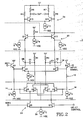
- a differential implementation of the electronic delay control circuit is illustrated in Fig. 2.
- the pulse signal to be delayed is input to emitter-follower transistor Q4 which serves to isolate the electronic delay control circuit from external circuits.
- the input pulse signal is applied as inputs to respective differential amplifier transistors Q3, Q6, Q8.
- a first reference signal REF1 is input via isolation transistor Q1 to the respective differential amplifier transistors Q2, Q5, Q7.
- the outputs of the differential amplifiers making up the second and third comparators 14, 16 are input to respective RC networks, R1C1 and R2C2, which make up the pulse shaping network 18.
- the outputs from the pulse shaping network 18 are summed with the outputs of the differential amplifier formed by Q2, Q3, which make up the first comparator 12, at nodes 28, 30.
- the summed output is input to the buffer differential amplifier 20 formed by transistors Q11, Q12 and then input to the differential output amplifier 22 formed by transistors Q13, Q14 to provide complementary outputs.
- the delay control signal and a second reference signal REF2 are input to the current steering differential amplifier 24 formed by transistors Q9, Q10.
- the current steering differential amplifier 24 is biased by the control current Ic.
- the delay control signal equals REF2
- the control current Ic is divided equally between the two comparators 14, 16.
- the pulse input signal therefore provides complementary output pulse signals at the collectors that have a nominal edge slope as shown by the solid line 32 in Fig. 3. If the delay control signal is greater than REF2 and a positive pulse signal is input, then more of Ic flows through comparator 16 than through comparator 14, causing the current input to the pulse shaping network 18 at the junction of R1C1 to increase and the current input at the junction of R2C2 to decrease.
- Fig. 4 illustrates the delay characteristics of the circuit of Fig. 2.
- the delay time is measured in picoseconds over a five volt control range. If REF2 is selected to be in the middle of the range where the characteristic is virtually linear, i.e., at approximately three volts, then a delay control signal in the range of approximately two to four volts provides a delay of approximately ⁇ four hundred and seventy five picoseconds.
- REF1 can be a constant value. However if the input pulse signal does not have the desired duty cycle, then the input pulse signal is converted into a ramp signal prior to input to the isolation transistor Q4. REF1 is then adjusted to provide the desired duty cycle for the output pulse signal. Such a pulse width control is independent of the delay controlled by the delay control signal.
- the present invention provides an electronic delay control circuit that effectively provides fine delay adjustment of an input pulse signal without varying its pulse width by adding current pulses to the output current pulse signal at the edges of the input pulse signal, the delay control signal causing a control current from a constant current source to be steered between two pulse shaping networks to generate the pulse currents.
Landscapes
- Physics & Mathematics (AREA)
- Nonlinear Science (AREA)
- Pulse Circuits (AREA)
Applications Claiming Priority (2)
| Application Number | Priority Date | Filing Date | Title |
|---|---|---|---|
| US07/208,450 US4862020A (en) | 1988-06-20 | 1988-06-20 | Electronic delay control circuit having pulse width maintenance |
| US208450 | 1988-06-20 |
Publications (2)
| Publication Number | Publication Date |
|---|---|
| EP0347983A2 true EP0347983A2 (fr) | 1989-12-27 |
| EP0347983A3 EP0347983A3 (fr) | 1990-10-10 |
Family
ID=22774657
Family Applications (1)
| Application Number | Title | Priority Date | Filing Date |
|---|---|---|---|
| EP19890201549 Withdrawn EP0347983A3 (fr) | 1988-06-20 | 1989-06-14 | Circuit électronique de commande de délai |
Country Status (3)
| Country | Link |
|---|---|
| US (1) | US4862020A (fr) |
| EP (1) | EP0347983A3 (fr) |
| JP (1) | JPH0239720A (fr) |
Cited By (5)
| Publication number | Priority date | Publication date | Assignee | Title |
|---|---|---|---|---|
| EP0562905A1 (fr) * | 1992-03-24 | 1993-09-29 | Bull S.A. | Circuit à retard variable |
| EP0562904A1 (fr) * | 1992-03-24 | 1993-09-29 | Bull S.A. | Procédé et dispositif de réglage de retard à plusieurs gammes |
| EP0613246A1 (fr) * | 1993-02-25 | 1994-08-31 | AT&T Corp. | Ligne à retard variable ayant une grande plage et oscillateur en anneau |
| EP0456231B1 (fr) * | 1990-05-11 | 1997-01-08 | Sony Corporation | Circuit de retard programmable |
| EP0998041A3 (fr) * | 1998-10-27 | 2004-11-24 | NEC Electronics Corporation | Circuit à retard variable |
Families Citing this family (13)
| Publication number | Priority date | Publication date | Assignee | Title |
|---|---|---|---|---|
| US5218363A (en) * | 1982-04-12 | 1993-06-08 | Lecroy Corporation | High-speed switching tree with input sampling pulses of constant frequency and means for varying the effective sampling rate |
| US4945261A (en) * | 1989-03-27 | 1990-07-31 | National Semiconductor Corporation | Level and edge sensitive input circuit |
| FR2655218A1 (fr) * | 1989-11-28 | 1991-05-31 | Radiotechnique Compelec | Circuit retardateur a retard reglable. |
| DE4110340C2 (de) * | 1990-04-16 | 1993-11-25 | Tektronix Inc | Aktive ansteuerbare digitale Verzögerungsschaltung |
| US5159205A (en) * | 1990-10-24 | 1992-10-27 | Burr-Brown Corporation | Timing generator circuit including adjustable tapped delay line within phase lock loop to control timing of signals in the tapped delay line |
| FR2671244B1 (fr) * | 1990-12-27 | 1993-03-05 | Bull Sa | Dispositif de retard reglable. |
| FR2671245B1 (fr) * | 1990-12-27 | 1993-03-05 | Bull Sa | Dispositif de retard reglable. |
| US5554950A (en) * | 1992-02-04 | 1996-09-10 | Brooktree Corporation | Delay line providing an adjustable delay in response to binary input signals |
| US5262690A (en) * | 1992-04-29 | 1993-11-16 | International Business Machines Corporation | Variable delay clock circuit |
| US5191301A (en) * | 1992-05-12 | 1993-03-02 | International Business Machines Corporation | Integrated differential voltage controlled ring oscillator |
| US5532622A (en) * | 1995-04-24 | 1996-07-02 | International Business Machines Corporation | Multi-input transition detector with a single delay |
| US6066972A (en) * | 1998-10-13 | 2000-05-23 | International Business Machines Corporation | Differential receiver with duty cycle asymmetry correction |
| US6411145B1 (en) * | 2001-06-14 | 2002-06-25 | Lsi Logic Corporation | Feedback control of clock duty cycle |
Family Cites Families (15)
| Publication number | Priority date | Publication date | Assignee | Title |
|---|---|---|---|---|
| DE2114149C3 (de) * | 1971-03-24 | 1973-09-20 | Robert Bosch Fernsehanlagen Gmbh, 6100 Darmstadt | Amphtudendiskriminator fur eine Schaltungsanordnung zur Erzeugung eines Korrektursignals zur Flankenverstelle rung von Impulsen |
| JPS5615168B2 (fr) * | 1973-08-28 | 1981-04-08 | ||
| US3906247A (en) * | 1974-01-16 | 1975-09-16 | Gte Automatic Electric Lab Inc | Programmable proportional clock edge delay circuit |
| JPS56147709A (en) * | 1980-04-18 | 1981-11-16 | Lion Corp | Tooth paste composition |
| DE3327427C2 (de) * | 1983-07-29 | 1985-11-21 | Schwabe GmbH & Co KG, 7067 Urbach | Generator für Rechteckspannungen variabler Phase |
| DE3483576D1 (de) * | 1983-12-09 | 1990-12-13 | Fujitsu Ltd | Tor-schaltungsanordnung. |
| US4567378A (en) * | 1984-06-13 | 1986-01-28 | International Business Machines Corporation | Driver circuit for controlling signal rise and fall in field effect transistor processors |
| JPS61290815A (ja) * | 1985-06-19 | 1986-12-20 | Victor Co Of Japan Ltd | 移相回路 |
| CA1242770A (fr) * | 1985-08-06 | 1988-10-04 | Mosaid Technologies Inc. | Generateur de signaux de synchronisation programmable |
| JPS62101116A (ja) * | 1985-10-29 | 1987-05-11 | Toko Inc | パルス遅延回路 |
| CA1270911A (fr) * | 1986-07-18 | 1990-06-26 | Einar O. Traa | Circuit a retard numerique rapide programmable |
| US4801827A (en) * | 1987-11-02 | 1989-01-31 | Tektronix, Inc. | Adjustable delay element for digital systems |
| US4797586A (en) * | 1987-11-25 | 1989-01-10 | Tektronix, Inc. | Controllable delay circuit |
| JP3769323B2 (ja) * | 1996-06-18 | 2006-04-26 | 積水化学工業株式会社 | 建物ユニットを用いたユニット建物の構築構造 |
| JPH117914A (ja) * | 1997-06-18 | 1999-01-12 | Ulvac Japan Ltd | イオン照射装置 |
-
1988
- 1988-06-20 US US07/208,450 patent/US4862020A/en not_active Expired - Fee Related
-
1989
- 1989-06-14 EP EP19890201549 patent/EP0347983A3/fr not_active Withdrawn
- 1989-06-15 JP JP1153575A patent/JPH0239720A/ja active Pending
Cited By (9)
| Publication number | Priority date | Publication date | Assignee | Title |
|---|---|---|---|---|
| EP0456231B1 (fr) * | 1990-05-11 | 1997-01-08 | Sony Corporation | Circuit de retard programmable |
| EP0562905A1 (fr) * | 1992-03-24 | 1993-09-29 | Bull S.A. | Circuit à retard variable |
| EP0562904A1 (fr) * | 1992-03-24 | 1993-09-29 | Bull S.A. | Procédé et dispositif de réglage de retard à plusieurs gammes |
| FR2689339A1 (fr) * | 1992-03-24 | 1993-10-01 | Bull Sa | Procédé et dispositif de réglage de retard à plusieurs gammes. |
| FR2690022A1 (fr) * | 1992-03-24 | 1993-10-15 | Bull Sa | Circuit à retard variable. |
| US5327031A (en) * | 1992-03-24 | 1994-07-05 | Bull S.A. | Variable-delay circuit |
| EP0613246A1 (fr) * | 1993-02-25 | 1994-08-31 | AT&T Corp. | Ligne à retard variable ayant une grande plage et oscillateur en anneau |
| US5434525A (en) * | 1993-02-25 | 1995-07-18 | At&T Corp. | Wide-range variable delay and ring oscillator |
| EP0998041A3 (fr) * | 1998-10-27 | 2004-11-24 | NEC Electronics Corporation | Circuit à retard variable |
Also Published As
| Publication number | Publication date |
|---|---|
| EP0347983A3 (fr) | 1990-10-10 |
| US4862020A (en) | 1989-08-29 |
| JPH0239720A (ja) | 1990-02-08 |
Similar Documents
| Publication | Publication Date | Title |
|---|---|---|
| US4862020A (en) | Electronic delay control circuit having pulse width maintenance | |
| US4988960A (en) | FM demodulation device and FM modulation device employing a CMOS signal delay device | |
| US5039893A (en) | Signal delay device | |
| US6624688B2 (en) | Filtering variable offset amplifer | |
| US4638255A (en) | Rectangular wave pulse generators | |
| EP0315376B1 (fr) | Elément de retard ajustable pour systèmes numériques | |
| US5317219A (en) | Compensated digital delay circuit | |
| US5306971A (en) | Binary controlled digital tapped delay line | |
| JPH07202653A (ja) | 時間遅延回路 | |
| US5334891A (en) | Variable delay circuit for producing a delay which varies as a hyperbolic function of the current intensity | |
| JPH0744438B2 (ja) | 遅延回路 | |
| EP0534638B1 (fr) | Système d'ajustage de la phase d'horloge à faible instabilité | |
| KR100937066B1 (ko) | 디지털 제어 펄스 폭 조정 회로 | |
| JPH0563525A (ja) | パルス幅可変回路 | |
| US4691120A (en) | Pulse delay circuit device | |
| US4710654A (en) | Delay circuit including an improved CR integrator circuit | |
| KR100400317B1 (ko) | 클럭 동기 장치의 지연 회로 | |
| US4747068A (en) | Adaptive filter | |
| JP2688552B2 (ja) | 可変遅延装置 | |
| US7872515B1 (en) | Phase interpolation device and slew rate control device thereof | |
| US5140283A (en) | Time variant analog signal switching apparatus including switching transient avoidance | |
| CA2040134C (fr) | Ligne a retard reglable | |
| US5155388A (en) | Logic gates with controllable time delay | |
| US6940331B2 (en) | Delayed tap signal generating circuit for controlling delay by interpolating two input clocks | |
| JP2664958B2 (ja) | クロックデューティ調整回路 |
Legal Events
| Date | Code | Title | Description |
|---|---|---|---|
| PUAI | Public reference made under article 153(3) epc to a published international application that has entered the european phase |
Free format text: ORIGINAL CODE: 0009012 |
|
| AK | Designated contracting states |
Kind code of ref document: A2 Designated state(s): CH LI NL |
|
| PUAL | Search report despatched |
Free format text: ORIGINAL CODE: 0009013 |
|
| AK | Designated contracting states |
Kind code of ref document: A3 Designated state(s): CH LI NL |
|
| 17P | Request for examination filed |
Effective date: 19901015 |
|
| 17Q | First examination report despatched |
Effective date: 19930505 |
|
| STAA | Information on the status of an ep patent application or granted ep patent |
Free format text: STATUS: THE APPLICATION IS DEEMED TO BE WITHDRAWN |
|
| 18D | Application deemed to be withdrawn |
Effective date: 19930916 |