EP0347862B1 - Entraîneur pour moteur sans balais - Google Patents
Entraîneur pour moteur sans balais Download PDFInfo
- Publication number
- EP0347862B1 EP0347862B1 EP89111244A EP89111244A EP0347862B1 EP 0347862 B1 EP0347862 B1 EP 0347862B1 EP 89111244 A EP89111244 A EP 89111244A EP 89111244 A EP89111244 A EP 89111244A EP 0347862 B1 EP0347862 B1 EP 0347862B1
- Authority
- EP
- European Patent Office
- Prior art keywords
- transistor
- transistors
- current
- driving
- driving transistors
- Prior art date
- Legal status (The legal status is an assumption and is not a legal conclusion. Google has not performed a legal analysis and makes no representation as to the accuracy of the status listed.)
- Expired - Lifetime
Links
Images

Classifications
-
- H—ELECTRICITY
- H02—GENERATION; CONVERSION OR DISTRIBUTION OF ELECTRIC POWER
- H02P—CONTROL OR REGULATION OF ELECTRIC MOTORS, ELECTRIC GENERATORS OR DYNAMO-ELECTRIC CONVERTERS; CONTROLLING TRANSFORMERS, REACTORS OR CHOKE COILS
- H02P6/00—Arrangements for controlling synchronous motors or other dynamo-electric motors using electronic commutation dependent on the rotor position; Electronic commutators therefor
- H02P6/08—Arrangements for controlling the speed or torque of a single motor
- H02P6/085—Arrangements for controlling the speed or torque of a single motor in a bridge configuration
-
- H—ELECTRICITY
- H02—GENERATION; CONVERSION OR DISTRIBUTION OF ELECTRIC POWER
- H02P—CONTROL OR REGULATION OF ELECTRIC MOTORS, ELECTRIC GENERATORS OR DYNAMO-ELECTRIC CONVERTERS; CONTROLLING TRANSFORMERS, REACTORS OR CHOKE COILS
- H02P6/00—Arrangements for controlling synchronous motors or other dynamo-electric motors using electronic commutation dependent on the rotor position; Electronic commutators therefor
- H02P6/34—Modelling or simulation for control purposes
-
- Y—GENERAL TAGGING OF NEW TECHNOLOGICAL DEVELOPMENTS; GENERAL TAGGING OF CROSS-SECTIONAL TECHNOLOGIES SPANNING OVER SEVERAL SECTIONS OF THE IPC; TECHNICAL SUBJECTS COVERED BY FORMER USPC CROSS-REFERENCE ART COLLECTIONS [XRACs] AND DIGESTS
- Y02—TECHNOLOGIES OR APPLICATIONS FOR MITIGATION OR ADAPTATION AGAINST CLIMATE CHANGE
- Y02P—CLIMATE CHANGE MITIGATION TECHNOLOGIES IN THE PRODUCTION OR PROCESSING OF GOODS
- Y02P80/00—Climate change mitigation technologies for sector-wide applications
- Y02P80/10—Efficient use of energy, e.g. using compressed air or pressurized fluid as energy carrier
Definitions
- the present invention relates to a brushless motor driver applicable to an acoustic apparatus and an image apparatus and the like.
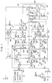
- Fig. 4 is a circuit diagram showing a conventional brushless motor driver.
- a brushless motor 1 has three phase driving coils 2a, 2b and 2c and a rotor (not shown), and driving transistors Q21, Q22, Q25, Q26, Q29 and Q30 are provided for controlling current supply to the driving coils 2a, 2b and 2c.
- the driving transistors Q21, Q25 and Q29 arranged at an upper side are NPN transistors respectively, whose collectors are connected with a positive feed terminal 3 of a power source V CC .
- the driving transistors Q22, Q26 and Q30 arranged at a lower side are NPN transistors respectively, whose emitters are connected to an inverting input terminal of a control amplifier A1 and to ground (negative feed terminal) through a resistance R11.
- An emitter of the driving transistor Q21 is connected with a collector of the driving transistor Q22, and the node between the both transistors Q21 and Q22 is connected with the driving coil 2a.
- An emitter of the driving transistor Q25 is connected with a collector of the driving transistor Q26, and the node between the both transistors Q25 and Q26 is connected with the driving coil 2b.
- An emitter of the driving transistor Q29 is connected with a collector of the driving transistor Q30, and the node between the both transistors Q29 and Q30 is connected with the driving coil 2c.
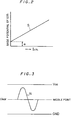
- Terminals 4 to 9 are provided for inputting sensor signals H U +, H U ⁇ , H V +, H V ⁇ , H W + and H W ⁇ as shown in Fig. 5 respectively, the sensor signals H U +, H U ⁇ , H V +, H V ⁇ , H W + and H W ⁇ being produced by well known technique on the basis of rotating angle of the rotor.
- the sensor signals H U +, H V +, H W + are 120 degrees out of phase to each other, while the sensor signals H U ⁇ , H V ⁇ and H W ⁇ are 180 degrees out of phase with the sensor signals H U +, H V + and H W + respectively.
- the terminals 4 and 5 are respectively connected with bases of NPN transistors Q1 and Q2 forming a differential transistor pair, and emitters of the transistors Q1 and Q2 are coupled and connected with ground through a constant current source 10.
- the terminals 6 and 7 are respectively connected with bases of NPN transistors Q4 and Q5 forming a differential transistor pair, and emitters of the transistors Q4 and Q5 are coupled and connected with ground through a constant current source 11.
- the terminals 8 and 9 are respectively connected with bases of NPN transistors Q7 and Q8 forming a differential transistor pair, and emitters of the transistors Q7 and Q8 are coupled and connected with ground through a constant current source 12.
- a collector of the transistor Q1 is connected with a collector and a base of a PNP transistor Q3 and a base of a PNP transistor Q12, and emitters of the transistors Q3 and Q12 are connected with the positive feed terminal 3 respectively.
- the transistors Q3 and Q12 form a current mirror circuit.
- a collector of the transistor Q4 is connected with a collector and a base of a PNP transistor Q6 and a base of a PNP transistor Q11, and emitters of the transistors Q6 and Q11 are connected with the positive feed terminal 3 respectively.
- the transistors Q6 and Q11 form a current mirror circuit.
- a collector of the transistor Q7 is connected with a collector and a base of a PNP transistor Q9 and a base of a PNP transistor Q10, and emitters of the transistors Q9 and Q10 are connected with the positive feed terminal 3 respectively.
- the transistors Q9 and Q10 form a current mirror circuit.
- Collectors of the transistors Q2 and Q9 are connected and collectors of the transistors Q5 and Q3 are connected while collectors of the transistors Q8 and Q6 are connected.
- a collector of the transistor Q10 is connected with ground through a resistance R1, and a collector of the transistor Q11 is connected with ground through a resistance R2 while a collector of the transistor Q12 is connected with ground through a resistance R3.
- a current corresponding to the current obtained by adding a current flowing through transistor Q1 and a current flowing through transistor Q5 flows through the resistance R3 via the transistors Q3 and Q12 forming-the current mirror circuit, and a voltage corresponding to a voltage drop across the resistance R3 can be output from a node N1 as an output voltage for U phase.
- a current corresponding to the one obtained by adding a current flowing through the transistor Q4 and a current flowing through the transistor Q8 flows through the resistance R2 via the transistors Q6 and Q11 forming the current mirror circuit, and a voltage corresponding to a voltage drop across the resistance R2 can be output from a node N2 as an output voltage for V phase.
- transistor Q2 flows through the resistance R1 via the transistors Q9 and Q10 forming the current mirror circuit, and a voltage corresponding to a voltage drop across the resistance R1 can be output from a node N3 as an output voltage for W phase.
- a waveform synthetic circuit 13 consists of the terminals 4 to 9, the transistors Q1 to Q12, the resistances R1 to R3 and the constant current sources 10 to 12.
- the node N1 of the output voltage for U phase is connected with both bases of a PNP transistor Q13 and an NPN transistor Q14, and the node N2 of the output voltage for V phase is connected with both bases of a PNP transistor Q15 and an NPN transistor Q16, while the node N3 of the output voltage for W phase is connected with both bases of a PNP transistor Q17 and an NPN transistor Q18.
- Emitters of the transistors Q13, Q15 and Q17 are commonly to the positive feed terminal 3 through a constant current source 14, and collectors of the transistors Q13, Q15 and Q17 are respectively connected with bases of the driving transistors Q22, Q26 and Q30 arranged on the lower side.
- Resistances R7, R8 and R9 are connected between bases and emitters of the driving transistors Q22, Q26 and Q30 respectively.
- operation of the transistors Q13, Q15 and Q17 is controlled on the basis of the output voltage of the nodes N1, N2 and N3 respectively to selectively supply a current of the constant current source 14 to the bases of the driving transistors Q22, Q26 and Q30 and the resistancesR7, R8 and R9, so that the operation of the driving transistors Q22, Q26 and Q30 can be controlled.
- emitters of the transistors Q14, Q16 and Q18 are commonly connected with ground through a constant current source 15.
- a collector of the transistor Q14 is connected with a base and a collector of a PNP transistor Q19 and a base of a PNP transistor Q20, and emitters of the transistors Q19 and Q20 are connected with the positive feed terminal 3, respectively.
- the transistors Q19 and Q20 provide a current mirror circuit.
- a collector of the transistor Q20 is connected with a base of the driving transistor Q21 while being connected with an emitter of the driving transistor Q21 through a resistance R4.
- a collector of the transistor Q16 is connected with a base and a collector of a PNP transistor Q23 and a base of a PNP transistor Q24, and emitters of the transistors Q23 and Q24 are connected with the positive feed terminal 3, respectively.
- the transistors Q23 and Q24 provide a current mirror circuit.
- a collector of the transistor Q24 is connected with a base of the driving transistor Q25 while being connected with an emitter of the driving transistor Q25 through a resistance R5.
- a collector of the transistor Q18 is connected with a base and a collector of a PNP transistor Q27 and a base of a PNP transistor Q28, and emitters of the transistors Q27 and Q28 are connected with the positive feed terminal 3.
- the transistors Q27 and Q28 consist of a current mirror circuit.
- a collector of the transistor Q28 is connected with a base of the driving transistor Q29 while being connected with an emitter of the driving transistor Q29 through a resistance R6.
- the transistors Q14, Q16 and Q18 are controlled on the basis of the output voltage of the nodes N1, N2 and N3, respectively, to selectively supply a current absorbed by the constant current source 15 to the transistors Q19, Q23 and Q27, to thereby selectively supply a current corresponding to the current flowing in the transistors Q19, Q23 and Q27 to the bases of the driving transistors Q21, Q25 and Q29 and the resistancesR4, R5 and R6 through the transistors Q20, Q24 and Q28, so that the driving transistors Q21, Q25 and Q29 can be controlled.
- a torque command V T is applied to a non-inverting input terminal thereof from a terminal 16.
- the control amplifier A1 adjusts the amount of current I CTL flowing in each of the constant current sources 14 and 15 so that a voltage R F across the resistance R11 is the same as the voltage of the torque command V T .
- the resistance 10 is provided for setting a DC-gain of the control amplifier A1 in cooperation with the resistance R11.
- the sensor signals H U +, H U ⁇ , H V +, H V ⁇ , H W + and H W ⁇ as shown in Fig. 5 are applied to the terminals 4 to 9 of the waveform synthetic circuit 13 in relation to the rotating angle ⁇ E of the rotor.
- a current I O of the constant current source 10 is fed to the transistors Q3 and Q9 in proportion to the base-to-emitter voltages of the transistors Q1 and Q2 forming the differential transistor pair.
- a current I O of the constant current source 11 is fed to the transistors Q6 and Q3 in proportion to the base-to-emitter voltages of the transistors Q4 and Q5 forming the differential transistor pair.
- a current I O of the constant current source 12 is fed to the transistors Q9 and Q6 in proportion to the base-to-emitter voltages of the transistors Q7 and Q8 forming the differential transistor pair.
- the current corresponding to the one obtained by adding the current flowing through the transistor Q1 and the current flowing through the transistor Q5 flows through the resistance R3 via the transistors Q3 and Q12 forming the current mirror circuit, to thereby set the potential of the node N1.
- the current corresponding to the one obtained by adding the current flowing through the transistor Q4 and the current flowing through the transistor Q8 flows through the resistance R2 via the transistors Q6 and Q11 forming the current mirror circuit, to thereby set the potential of the node N2.
- the current corresponding to the one obtained by adding the current flowing through the transistor Q7 and the current flowing through the transistor Q2 flows through the resistance R1 via the transistors Q9 and Q10 forming the current mirror circuit, to thereby set the potential of the node N3.
- the potential of the node N1 is "H" when the voltages of the sensor signals H U +, H U ⁇ , H V + and H V ⁇ have the relation of H U + > H U ⁇ , H V ⁇ > H V + (namely, the rotating angle ⁇ E is within the range from O° to 120°), while the potential is "L" when the voltages of the sensor signals H U +, H U ⁇ , H V ⁇ and H V + have the relation of H U + ⁇ H U ⁇ , H V ⁇ ⁇ H V + (namely, the rotating angle ⁇ E is within the range from 180° to 300°).
- the transistor Q14 When the level of the node N1 is "H”, the transistor Q14 conducts to supply the current corresponding to the current flowing through the transistor Q14 to the base of the driving transistor Q21 and the resistance R4 through transistors Q19 and Q20 forming the current mirror circuit, so that the driving transistor Q21 is turned on.
- the transistor Q13 when the level of the node N2 is "L”, the transistor Q13 conducts to supply a current to the base of the driving transistor Q22 and the resistance R7, so that the driving transistor Q22 is turned on.
- the potential of the node N2 is "H" when the voltages of the sensor signals H V +, H V ⁇ , H W + and H W ⁇ have the relation of H V + > H V ⁇ , H W ⁇ > H W + (namely, the rotating angle ⁇ E is within the range from 120° to 240°), so that the driving transistor Q25 is turned on by the transistors Q16, Q23 and Q24.
- the potential of the node N2 is "L" when the voltages of the sensor signals H V +, H V ⁇ , H W + and H W ⁇ have the relation of H V + ⁇ H V ⁇ , H W ⁇ ⁇ H W + (namely, the rotating angle ⁇ E is within the range from O° to 60° and 300° to 360°), so that the driving transistor Q26 is turned on by the transistor Q15.
- the potential of the node N3 is "H" when the voltages of the sensor signals H W +, H W ⁇ , H U + and H U ⁇ have the relation of H W + > H W ⁇ , H U ⁇ > H U + (namely, the rotating angle ⁇ E is within the range from 240° to 360°), so that the driving transistor Q29 is turned on by the transistor Q18, Q27 and Q28.
- the potential of the node N3 is "L" when the voltages of the sensor signals H W +, H W ⁇ , H U + and H U ⁇ have the relation of H W + ⁇ H W ⁇ , H U ⁇ ⁇ H U + (namely, the rotating angle ⁇ E is within the range from 60° to 180°), so that the driving transistor Q30 is turned on by the transistor Q17.
- the driving transistors Q21, Q25 and Q29 arranged on the upper side and the driving transistors Q22, Q26 and Q30 arranged on the lower side are sequentially turned on by switching every rotating angle 120° on the basis of the sensor signals H U +, H U ⁇ , H V +, H V ⁇ , H W + and H W ⁇ , whereby the current sequentially flows to driving coils 2a, 2b and 2c so as to obtain a rotating magnetic field for producing a moment of rotation.
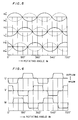
- Fig. 6 shows the current inflow-outflow state of the brushless motor 1 in U phase, V phase and W phase.
- the currents I CTL of the constant current sources 14 and 15 are adjusted by the control amplifier A1 so that a driving current corresponding to the torque command V T flows to the driving coils 2a, 2b and 2c. Namely, when the voltage of the torque command V T rises, the currents I CTL of the constant current sources 14 and 15 are increased by the operation of the control amplifier A1, whereby the base currents of the driving transistors Q21, Q22, Q25, Q26, Q29 and Q30 are increased to increase the driving current flowing in the driving coils 2a, 2b and 2c.
- the driving current causes the voltage R F to rise by flowing in the resistance R11.
- Another brushless motor driver is disclosed in the patent publication JP-A 58-33988.
- the motor is controlled by applying signals of the rotor position to differential amplifiers.
- the voltage of a reference voltage generator is compared with the outputs of transistors, which detect the operating voltages of coil drive transistors, thereby controlling the currents of the transistors through a current mirror circuit, a transistor and a condenser of a low pass filter.
- the arrangement is provided to prevent oversaturation of the coil drive transistors.
- a principal object of the present invention is to provide an improved brushless motor driver which can drive the motor with a high efficiency and a low noise while preventing saturation of driving transistors with respect to any torque command.
- a brushless motor driver is provided as defined in claim 1.
- the brushless motor driver comprises a brushless motor having a rotor and driving coils for polyphase; control signal producing means for producing transistor drive control signals per each phase on the basis of the rotating angle of the rotor; means for applying a torque command; current adjusting means for adjusting an amount of current in the transistor drive control signals on the basis of the torque command; a group of driving transistors, each of the driving transistors having a control electrode, for driving the rotor by controlling current with respect to the driving coils on the basis of the transistor drive control signals applied to each of the control electrodes; saturation voltage generating means for generating a saturation voltage corresponding to the torque command; and current correcting means for comparing the saturation voltage generated by the saturation voltage generating means with an operating voltage of each the driving transistors to correct the amount of current in the transistor drive control signals so that the operating voltage drops below the saturation voltage generator by the saturation voltage generating means.
- the saturation voltage corresponding to the torque command is generated and compared with the operating voltage of each of the driving transistors to correct the value of current in the transistor drive control signals so that the operating voltage drops below the generated saturation voltage, for driving the motor with high efficiency and low noise while preventing saturation of the driving transistors at any torque command.
- Fig. 1 is a circuit diagram showing a brushless motor driver according to an embodiment of the present invention.
- the same reference numerals as in Fig. 4 designate identical or equivalent parts.
- a PNP transistor Q49 in lieu of the constant current source 14 in Fig. 4 is connected to emitters of the transistors Q13, Q15 and Q17, while an NPN transistor Q50 in lieu of the constant current source 15 in Fig. 4 is connected to emitters of the transistors Q14, Q16 and Q18.
- a constant current source 17 is further provided in which an amount or value of a current I CTL is controlled by the control amplifier A1.
- a current distributing circuit which consists of transistors Q39 to Q48 is also provided between the constant current source 17 and the transistors Q49 and Q50.
- one end of the constant current source 17 is connected with the positive feed terminal 3 while another end thereof is connected with a collector and a base of an NPN transistor Q39 and a base of an NPN transistor Q40. Emitters of the transistors Q39 and Q40 are connected with ground respectively, thus the transistors Q39 and Q40 form a current mirror circuit.
- a collector of the transistor Q40 is connected with a collector and a base of a PNP transistor Q41 and a base of a PNP transistor Q42, while emitters of the transistors Q41 and Q42 are connected with the positive feed terminal 3 respectively, thus the transistors Q41 and Q42 form a current mirror circuit.
- a collector of the transistor Q42 is connected with emitters of PNP transistors Q43 and Q44 forming a differential transistor pair.
- a reference voltage V REF is applied to a base of the transistor Q43 from a voltage source 18, while an output voltage V O of an error amplifier A2 is applied to a base of the transistor Q44, so that a current flowing in the transistor Q42 may be distributed to the transistors Q43 and Q44 according to the voltages V REF at the basis of Q43 and V O at the basis of Q44.
- a collector of the transistor Q43 is connected with a collector and a base of an NPN transistor Q45 and a base of the NPN transistor Q50, while emitters of the transistors Q45 and Q50 are connected with ground respectively, thus the transistors Q45 and Q50 form a current mirror circuit.
- a collector of the transistor Q44 is connected with a collector and a base of an NPN transistor Q46 and a base of an NPN transistor Q47, while emitters of the transistors Q46 and Q47 are connected with ground respecetively, thus the transistors Q46 and Q47 form a current mirror circuit.
- a collector of the transistor Q47 is connected with a collector and a base of a PNP transistor Q48 and a base of the PNP transistor Q49, while emitters of the transistors Q48 and Q49 are connected with the positive feed terminal 3 respectively, thus the transistors Q48 and Q49 form a current mirror circuit.
- a current corresponding to a current supplied to the transistor Q39 from the constant current source 17 flows to the transistor Q42 through the transistors Q40 and Q41.
- a current flowing in the transistor Q42 is distributed to the transistors Q43 and Q44 according to the voltages V REF and V O .
- a current corresponding to a current flowing in the transistor Q43 flows in the transistor Q50 through the transistor Q45, while a current corresponding to the current flowing in the transistor Q44 flows in the transistor Q49 through the transistors Q46, Q47 and Q48.
- An amplification circuit 19 consists of an error amplifier A2, a voltage source 18 for generating a reference voltage V REF , and resistances R15 and R16.
- the reference voltage V REF from the voltage source 18 is in addition to Q43 also fed to a non-inverting input terminal of the error amplifier A2.
- a potential (a motor driving output voltage for U phase) of a node between the driving transistors Q21 and Q22 is inputted through resistances R12 and R15
- a potential (a motor driving output voltage for V phase) of a node between the driving transistors Q25 and Q26 is inputted through resistances R13 and R15
- a potential (a motor driving output voltage for W phase) of a node between the driving transistors Q29 and Q30 is inputted through resistances R14 and R15, respectively.
- the error amplifier A2 produces the voltage V O by amplifying the difference between the reference voltage V REF and the motor driving output voltage with a gain corresponding to the ratio of the resistance R16 to the resistance R15, and supplies the voltage V O to the base of the transistor Q44 so that the sum of the motor driving output voltages becomes equal to the reference voltage V REF .
- a saturation voltage generating circuit 22 consists of constant current sources 20 and 21, a diode Q34, and a resistance R17.
- One end of the constant current source 20 for supplying the current I CTL and one end of the constant current source 21 for supplying a current I1 are connected to the positive feed terminal 3 respectively, while the other ends of the constant current sources 20 and 21 are connected with an anode of the diode 34 respectively.
- a cathode of the diode 34 is connected with the emitters of the driving transistors Q22, Q26 and Q30 through the resistance R17.
- a constant current source 23 and diodes Q31, Q32 and Q33 are provided for detecting operating voltages (collector-to-emitter voltages) of the driving transistors Q22, Q26 and Q30 arranged at the lower side.
- one end of the constant current source 23 for supplying a current I1 is connected with the positive feed terminal 3
- the other end of the constant current source 23 is connected with anodes of the diodes Q31, Q32 and Q33
- cathodes of the diodes Q31, Q32 and Q33 are connected with the collectors of the driving transistors Q22, Q26 and Q30 respectively.
- a current correcting circuit 25 consists of transistors Q35 to Q38, and a constant current source 24 for correcting the base currents of the driving transistors Q21, Q22, Q25, Q26, Q29 and Q30.
- one end of the constant current source 24 for supplying a current I CTL is connected with the positive feed terminal 3, while the other end of the constant current source 24 is connected with emitters of PNP transistors Q35 and Q36 forming a differential transistor pair.
- a base of the transistor Q35 is connected with a node between the constant current source 20 and the diode Q34, while a base of the transistor Q36 is connected with a node between the constant current source 23 and the diodes Q31, Q32 and Q33.
- a collector of the transistor Q35 is connected with ground while a collector of the transistor Q36 is connected with a collector and a base of an NPN transistor Q37 and a base of an NPN transistor Q38.
- Emitters of transistors Q37 and Q38 are connected with ground respectively, while the collector of the transistor Q38 is connected with a collector of the transistor Q39, thus the transistors Q37 and Q38 form a current mirror circuit.
- the base potential of the transistor Q35 is the sum of the voltage R F across the resistance R11, the voltage across the resistance R17, and the voltage across the diode Q34.
- the base potential has a characteristic shown by a solid line S with respect to the current I CTL .
- reference numeral ⁇ designates a rising component of the base potential on the basis of the current I1 supplied from the constant current source 21.
- the rising component ⁇ is set for generating the saturation voltage which is slightly higher than the actual saturation voltage of the driving transistors.
- the base potential of the transistor Q36 is the sum of the voltage R F across the resistance R11, the operating voltage of the driving transistor Q22, Q26 or Q30, and the voltage across the diode Q31, Q32 or Q33.
- the saturation of the driving transistor is practically detected by the voltage across the resistance R17. Namely, when the operating voltage of the driving transistor drops below the voltage across the resistance R17 by the saturation of the driving transistor, the base potential of the transistor Q36 becomes less than the base potential of the transistor Q35, whereby the current I CTL of the constant current source 24 is divided into the transistor Q36 on the basis of the differential characteristic of the transistors Q35 and Q36.
- the transistors Q37 and Q38 forming the current mirror circuit, a current corresponding to a current flowing in the transistor Q36 is absorbed from the constant current source 17 into ground through the transistor Q38.
- the base potential of the transistor Q36 is higher than the base potential of the transistor Q35, and hence all the current I CTL of the constant current source 24 flows to the transistor Q35, to thereby prevent the current I CTL of the constant current source 17 from being absorbed by the transistor Q38.
- the current corresponding to the current I CTL flowing in the transistor Q39 flows to the transistor Q42 through the transistors Q40 and Q41, and the current flowing in the transistor Q42 is divided in the ratio 1:1 for supplying to the transistors Q43 and Q44, whereby the current corresponding to the current flowing in the transistor Q43 flows to the transistor Q50 through the transistor Q45, while the current corresponding to the current flowing in the transistor Q44 flows to the transistor Q49 through the transistors Q46, Q47 and Q48.
- the base currents corresponding to the torque command V T are supplied to the driving transistors Q21, Q22, Q25, Q26, Q29 and Q30, whereby the driving currents corresponding to the torque command V T are supplied to the driving coils 2a, 2b and 2c.
- the current supplied to the transistor Q39 from the constant current source 17 decreases to cause the currents of the transistors Q49 and Q50 to decrease, whereby the base currents of the driving transistors Q21, Q22, Q25, Q26, Q29 and Q30 decrease to prevent the driving transistors from saturating.
- the sum of the motor driving output voltages for U ⁇ W phase is adjusted so as to correspond with the reference voltage V REF by the amplification circuit 19 and the transistors Q43 and Q44 forming the differential circuit. Namely, if the sum of the motor driving output voltages becomes higher than the reference voltage V REF , the increased voltage is amplified by the amplification circuit 19 to cause the base potential V O of the transistor Q44 to drop, whereby the current flowing in the transistor Q50 decreases while the current flowing in the transistor Q49 increases on the basis of the differential characteristic of the transistors Q43 and Q44.
- the base currents of the driving transistors Q21, Q25 and Q29 arranged at the upper side decrease to cause the operating voltages (collector-to-emitter voltages) of the driving transistors Q21, Q25 and Q29 to rise, while the base currents of the driving transistors Q22, Q26 and Q30 arranged at the lower side increase to cause the operating voltages (collector-to-emitter voltages) of the driving transistors Q22, Q26 and Q30 to drop, whereby the motor driving output voltages of U ⁇ W phases drop.
- the decreased voltage is amplified by the amplification circuit 19 to cause the base potential V O of the transistor Q44 to rise, whereby the current flowing in the transistor Q50 increases while the current flowing in the transistor Q49 decreases on the basis of the differential characteristic of the transistors Q43 and Q44.
- the base currents of the driving transistors Q21, Q25 and Q29 arranged at the upper side increase to cause the operating voltages of the driving transistors Q21, Q25 and Q29 to drop, while the base currents of the driving transistors Q22, Q26 and Q30 arranged at the lower side decrease to cause the operating voltages of the driving transistors Q22, Q26 and Q30 to rise, whereby the motor driving output voltages of U ⁇ W phases rise.
- the sum of the motor driving output voltages for U ⁇ W phases is adjusted so as to correspond with the reference voltage V REF .
- Fig. 3 shows a motor driving waveform N in which the middle point thereof is set at the reference voltage V REF .
- the driving transistors Q21, Q22, Q25, Q26, Q29 and Q30 are prevented from saturating.
- V REF V CC - (V CE3 + V CE2 ) 2
- the driving transistors arranged at the upper side can be formed as a PNP output circuit.
- the saturation of the driving transistors Q22, Q26 and Q30 arranged at the lower side for adjust the motor driving output voltages of U ⁇ W phases is detected by means of the amplification circuit 19 and transistors Q43 and Q44 so that the driving transistors Q21, Q25 and Q29 arranged at the upper side can be prevented from saturation.
- the saturation of the driving transistors Q21, Q25 and Q29 arranged at the upper side for adjusting the motor driving output voltages of U ⁇ W phases may be detected by means the amplification circuit 19 and transistors Q43 and Q44 so that the driving transistors Q22, Q26 and Q30 arranged at the lower side can also be prevented from saturation.
Claims (3)
- Dispositif d'entraînement pour moteur sans balais, comprenant :
un moteur sans balais comportant un rotor et des bobines d'entraînement (2a, 2b, 2c) pour un système polyphasé ;
des moyens générateurs de signaux de commande (13) pour produire des signaux de commande de transistor pour chaque phase sur la base de l'angle de rotation dudit rotor ;
des transistors de commande (Q21, Q22, Q25, Q26, Q29, Q30) pour commander le courant d'alimentation desdites bobines d'entraînement (2a, 2b, 2c) sur la base desdits signaux de commande de transistor ;
des moyens (16) pour appliquer une commande de couple ;
des moyens d'ajustage de courant (A1, R10, R11, Q39 - Q50, 17) pour ajuster une quantité de courant s'écoulant dans lesdits transistors de commande sur la base de ladite commande de couple (VT) ;
des moyens générateurs de tension de saturation (22) pour engendrer une tension de saturation correspondant à ladite commande de couple (VT) ; et
des moyens de correction de courant (25) pour comparer ladite tension de saturation à une tension de fonctionnement desdits transistors de commande (Q21, Q22, Q25, Q26, Q29, Q30) pour corriger la quantité de courant s'écoulant dans lesdits transistors de commande, qui est ajustée par lesdits moyens d'ajustage de courant de façon que ladite tension de fonctionnement tombe en dessous de ladite tension de saturation,
caractérisé en ce que
ledit dispositif d'entraînement de moteur sans balais comprend en outre une borne d'alimentation positive (3) et une borne d'alimentation négative (RF),
lesdits transistors de commande comportent un groupe de premiers transistors de commande (Q21, Q25, Q29) connectés entre ladite borne d'alimentation positive (3) et chacune desdites bobines d'entraînement (2a, 2b, 2c) respectivement, et un groupe de seconds transistors de commande (Q22, Q26, Q30) connectés entre ladite borne d'alimentation négative (RF) et chacun desdites bobines d'entraînement (2a, 2b, 2c) respectivement,
lesdits moyens de correction de courant (25) comparent ladite tension de fonctionnement d'au moins l'un desdits groupes de premiers transistors d'entraînement (Q21, Q25, Q29) et de seconds transistors d'entraînement (Q22, Q26, Q30), à ladite tension de saturation,
ledit dispositif d'entraînement de moteur sans balais comprend en outre des moyens de circuit amplificateur (19) pour ajuster le rapport des courants s'écoulant dans ledit groupe de premiers transistors de commande (Q21, Q25, Q29) et ledit groupe de seconds transistors de commande (Q22, Q26, Q30) de façon que le potentiel des noeuds entre lesdits premiers transistors de commande et lesdits seconds transistors de commande soit sensiblement égal à une tension de référence (VREF), lesdits moyens de circuit (19) étant arrangés pour comparer ledit potentiel des noeuds entre lesdits premiers transistors de commande et lesdits seconds transistors de commande à ladite tension de référence (VREF). - Dispositif d'entraînement pour moteur sans balais selon la revendication 1, caractérisé en ce que
lesdits moyens générateurs de tension de saturation (22) comprenant :
des sources de courant constant (20, 21) pour engendrer une quantité de courant correspondant à ladite commande de couple (VT) ; et
une résistance (R17) montée en série avec lesdites sources de courant constant (20, 21) pour engendrer une tension de saturation comme fonction d'un courant fourni par lesdites sources de courant constant (20, 21). - Dispositif d'entraînement pour moteur sans balais selon la revendication 1, caractérisé en ce que les moyens de correction de courant précité (25) comprennent :
une source de courant constant (24) pour engendrer une quantité de courant correspondant à la commande de couple précité (VT) ;
une paire de transistors différentiels (Q35, Q36) qui se compose de deux transistors (Q35, Q36) reliés à ladite source de courant constant (24), respectivement, pour distribuer le courant fourni par ladite source de courant constant (24) à chacun des deux transistors (Q35, Q36) comme fonction de la tension de saturation précitée engendrée par les moyens générateur de tension de saturation précités (22) et la tension de fonctionnement précitée du groupe précité de transistors de commande ; et
un circuit symétrique de courant (Q37, Q38) relié à un transistor (36) de ladite paire de transistors différentiels (Q35, Q36) pour corriger une quantité de courant s'écoulant dans ledit groupe de transistors de commande, comme fonction du courant s'écoulant dans ledit transistor (Q36) lorsque ladite tension de fonctionnement dudit groupe de transistors de commande tombe en dessous de la tension de saturation engendrée par lesdits moyens générateurs de tension de saturation (22).
Applications Claiming Priority (2)
| Application Number | Priority Date | Filing Date | Title |
|---|---|---|---|
| JP153089/88 | 1988-06-20 | ||
| JP63153089A JPH0223090A (ja) | 1988-06-20 | 1988-06-20 | ブラシレスモータの駆動装置 |
Publications (3)
| Publication Number | Publication Date |
|---|---|
| EP0347862A2 EP0347862A2 (fr) | 1989-12-27 |
| EP0347862A3 EP0347862A3 (en) | 1990-12-05 |
| EP0347862B1 true EP0347862B1 (fr) | 1995-02-01 |
Family
ID=15554733
Family Applications (1)
| Application Number | Title | Priority Date | Filing Date |
|---|---|---|---|
| EP89111244A Expired - Lifetime EP0347862B1 (fr) | 1988-06-20 | 1989-06-20 | Entraîneur pour moteur sans balais |
Country Status (4)
| Country | Link |
|---|---|
| US (1) | US4987352A (fr) |
| EP (1) | EP0347862B1 (fr) |
| JP (1) | JPH0223090A (fr) |
| DE (1) | DE68920917T2 (fr) |
Families Citing this family (15)
| Publication number | Priority date | Publication date | Assignee | Title |
|---|---|---|---|---|
| US5115174A (en) * | 1989-01-18 | 1992-05-19 | Hitachi, Ltd. | Method of controlling brushless DC motor |
| US5173645A (en) * | 1989-07-03 | 1992-12-22 | Sankyo Seiki Mfg. Co., Ltd. | Brushless motor drive circuit |
| JP2633984B2 (ja) * | 1990-10-12 | 1997-07-23 | 株式会社三協精機製作所 | ブラシレスモータの駆動回路 |
| JP2634941B2 (ja) * | 1990-10-15 | 1997-07-30 | 株式会社三協精機製作所 | ブラシレスモータの駆動回路 |
| US5103148A (en) * | 1990-11-06 | 1992-04-07 | Motorola, Inc. | Low voltage circuit to control high voltage transistor |
| JP2624382B2 (ja) * | 1991-01-21 | 1997-06-25 | 株式会社三協精機製作所 | ブラシレスモータの駆動回路 |
| US5264774A (en) * | 1991-07-23 | 1993-11-23 | Rohm Co., Ltd. | Motor control circuit and motor drive system using the same |
| JPH06165571A (ja) * | 1992-11-18 | 1994-06-10 | Matsushita Electric Ind Co Ltd | ブラシレスモータの制御装置 |
| JP3367717B2 (ja) * | 1993-08-03 | 2003-01-20 | 株式会社リケン | 直流モータ制御回路及び直流モータ |
| US5668449A (en) * | 1994-10-27 | 1997-09-16 | Sgs-Thomson Microelectronics, Inc. | Motor with input-controlled high side driver |
| US5614797A (en) * | 1995-02-28 | 1997-03-25 | Sgs-Thomson Microelectronics, Inc. | Stator coil driver circuit for a brushless DC motor |
| US5731670A (en) * | 1995-03-31 | 1998-03-24 | Sgs-Thomson Microelectronics S.R.L. | Method for driving a brushless DC electric motor |
| JPH10290593A (ja) * | 1997-04-15 | 1998-10-27 | Mitsubishi Electric Corp | センサレス・ブラシレスモータの駆動回路 |
| US5883479A (en) * | 1997-07-01 | 1999-03-16 | Stmicroelectronics, Inc. | BEMF rectification during power off to prevent parasitic effect |
| JP2004222400A (ja) * | 2003-01-14 | 2004-08-05 | Mitsumi Electric Co Ltd | 電流制御回路、及び、モータ駆動回路 |
Family Cites Families (6)
| Publication number | Priority date | Publication date | Assignee | Title |
|---|---|---|---|---|
| JPS56123793A (en) * | 1980-02-29 | 1981-09-29 | Sony Corp | Driving circuit for brushless motor |
| JPS5833986A (ja) * | 1981-08-20 | 1983-02-28 | Matsushita Electric Ind Co Ltd | ブラシレス直流モ−タ |
| JPS5833987A (ja) * | 1981-08-21 | 1983-02-28 | Matsushita Electric Ind Co Ltd | ブラシレス直流モ−タ |
| JPS5833988A (ja) * | 1981-08-22 | 1983-02-28 | Matsushita Electric Ind Co Ltd | ブラシレス直流モ−タ |
| US4535276A (en) * | 1983-01-12 | 1985-08-13 | Matsushita Electric Industrial Co., Ltd. | Output circuit and brushless motor using the same |
| JPS59204485A (ja) * | 1983-05-04 | 1984-11-19 | Matsushita Electric Ind Co Ltd | ブラシレスモ−タの駆動装置 |
-
1988
- 1988-06-20 JP JP63153089A patent/JPH0223090A/ja active Pending
-
1989
- 1989-03-14 US US07/323,393 patent/US4987352A/en not_active Expired - Fee Related
- 1989-06-20 EP EP89111244A patent/EP0347862B1/fr not_active Expired - Lifetime
- 1989-06-20 DE DE68920917T patent/DE68920917T2/de not_active Expired - Fee Related
Also Published As
| Publication number | Publication date |
|---|---|
| EP0347862A2 (fr) | 1989-12-27 |
| JPH0223090A (ja) | 1990-01-25 |
| DE68920917T2 (de) | 1995-05-24 |
| EP0347862A3 (en) | 1990-12-05 |
| US4987352A (en) | 1991-01-22 |
| DE68920917D1 (de) | 1995-03-16 |
Similar Documents
| Publication | Publication Date | Title |
|---|---|---|
| EP0347862B1 (fr) | Entraîneur pour moteur sans balais | |
| US4958948A (en) | System for driving a brushless motor | |
| US4227127A (en) | Motor speed control circuit having improved starting characteristics | |
| KR100328418B1 (ko) | 센서리스브러쉬리스모터의구동회로 | |
| US4500830A (en) | Current control circuit for a plurality of loads | |
| JPS6311877B2 (fr) | ||
| US4626702A (en) | Saw-tooth wave generating circuit | |
| US4051428A (en) | Current control circuit with current proportional circuit | |
| JP3675371B2 (ja) | 電圧レギュレータ | |
| JP3016317B2 (ja) | 可変利得増幅器 | |
| US4788478A (en) | Speed control system for DC motor | |
| US4272709A (en) | Circuit for controlling the drive of motor | |
| JPH10163770A (ja) | 直流制御差動ベース電圧発生回路 | |
| US5907260A (en) | Differential amplifying circuit | |
| US5793170A (en) | Motor drive circuit | |
| US4511833A (en) | Stepping motor driving circuit | |
| US5014020A (en) | Amplifier for outputting motor controlling signal in motor controlling circuit | |
| KR940000866Y1 (ko) | 모터 유기전압의 중점 귀환회로 | |
| US4230980A (en) | Bias circuit | |
| JPS6227639B2 (fr) | ||
| JP2568690B2 (ja) | 定電流回路 | |
| US6130582A (en) | Amplifier circuit including compensation circuitry for canceling variations in an amplifier feedback signal | |
| JP2746574B2 (ja) | 速度サーボ回路 | |
| JPH0686587A (ja) | ブラシレスモータの駆動装置 | |
| JPH0618011B2 (ja) | 直流基準電圧発生回路 |
Legal Events
| Date | Code | Title | Description |
|---|---|---|---|
| PUAI | Public reference made under article 153(3) epc to a published international application that has entered the european phase |
Free format text: ORIGINAL CODE: 0009012 |
|
| AK | Designated contracting states |
Kind code of ref document: A2 Designated state(s): DE FR NL |
|
| PUAL | Search report despatched |
Free format text: ORIGINAL CODE: 0009013 |
|
| AK | Designated contracting states |
Kind code of ref document: A3 Designated state(s): DE FR NL |
|
| 17P | Request for examination filed |
Effective date: 19901212 |
|
| 17Q | First examination report despatched |
Effective date: 19921111 |
|
| GRAA | (expected) grant |
Free format text: ORIGINAL CODE: 0009210 |
|
| AK | Designated contracting states |
Kind code of ref document: B1 Designated state(s): DE FR NL |
|
| REF | Corresponds to: |
Ref document number: 68920917 Country of ref document: DE Date of ref document: 19950316 |
|
| ET | Fr: translation filed | ||
| PLBE | No opposition filed within time limit |
Free format text: ORIGINAL CODE: 0009261 |
|
| STAA | Information on the status of an ep patent application or granted ep patent |
Free format text: STATUS: NO OPPOSITION FILED WITHIN TIME LIMIT |
|
| 26N | No opposition filed | ||
| REG | Reference to a national code |
Ref country code: FR Ref legal event code: D6 |
|
| PGFP | Annual fee paid to national office [announced via postgrant information from national office to epo] |
Ref country code: FR Payment date: 19990610 Year of fee payment: 11 |
|
| PGFP | Annual fee paid to national office [announced via postgrant information from national office to epo] |
Ref country code: DE Payment date: 19990618 Year of fee payment: 11 |
|
| PGFP | Annual fee paid to national office [announced via postgrant information from national office to epo] |
Ref country code: NL Payment date: 19990628 Year of fee payment: 11 |
|
| PG25 | Lapsed in a contracting state [announced via postgrant information from national office to epo] |
Ref country code: NL Free format text: LAPSE BECAUSE OF NON-PAYMENT OF DUE FEES Effective date: 20010101 |
|
| PG25 | Lapsed in a contracting state [announced via postgrant information from national office to epo] |
Ref country code: FR Free format text: LAPSE BECAUSE OF NON-PAYMENT OF DUE FEES Effective date: 20010228 |
|
| NLV4 | Nl: lapsed or anulled due to non-payment of the annual fee |
Effective date: 20010101 |
|
| REG | Reference to a national code |
Ref country code: FR Ref legal event code: ST |
|
| PG25 | Lapsed in a contracting state [announced via postgrant information from national office to epo] |
Ref country code: DE Free format text: LAPSE BECAUSE OF NON-PAYMENT OF DUE FEES Effective date: 20010403 |