EP0347704A1 - Infrarotdetektor - Google Patents
Infrarotdetektor Download PDFInfo
- Publication number
- EP0347704A1 EP0347704A1 EP89110605A EP89110605A EP0347704A1 EP 0347704 A1 EP0347704 A1 EP 0347704A1 EP 89110605 A EP89110605 A EP 89110605A EP 89110605 A EP89110605 A EP 89110605A EP 0347704 A1 EP0347704 A1 EP 0347704A1
- Authority
- EP
- European Patent Office
- Prior art keywords
- components
- housing
- infrared
- detector
- infrared detector
- Prior art date
- Legal status (The legal status is an assumption and is not a legal conclusion. Google has not performed a legal analysis and makes no representation as to the accuracy of the status listed.)
- Granted
Links
- 230000005855 radiation Effects 0.000 claims abstract description 5
- 239000002991 molded plastic Substances 0.000 claims 1
- 229910052751 metal Inorganic materials 0.000 abstract description 8
- 239000002184 metal Substances 0.000 abstract description 8
- 238000000465 moulding Methods 0.000 abstract 1
- 238000010137 moulding (plastic) Methods 0.000 abstract 1
- 238000012216 screening Methods 0.000 abstract 1
- 241000239290 Araneae Species 0.000 description 5
- 238000004519 manufacturing process Methods 0.000 description 3
- 239000000463 material Substances 0.000 description 3
- 239000004033 plastic Substances 0.000 description 3
- IJGRMHOSHXDMSA-UHFFFAOYSA-N Atomic nitrogen Chemical compound N#N IJGRMHOSHXDMSA-UHFFFAOYSA-N 0.000 description 2
- 239000000853 adhesive Substances 0.000 description 2
- 230000001070 adhesive effect Effects 0.000 description 2
- 238000007765 extrusion coating Methods 0.000 description 2
- 230000005669 field effect Effects 0.000 description 2
- 229920001169 thermoplastic Polymers 0.000 description 2
- 229920001187 thermosetting polymer Polymers 0.000 description 2
- 239000004416 thermosoftening plastic Substances 0.000 description 2
- 239000003990 capacitor Substances 0.000 description 1
- 239000000919 ceramic Substances 0.000 description 1
- 239000013078 crystal Substances 0.000 description 1
- 238000007872 degassing Methods 0.000 description 1
- 238000010586 diagram Methods 0.000 description 1
- 230000009977 dual effect Effects 0.000 description 1
- 230000000694 effects Effects 0.000 description 1
- 238000005516 engineering process Methods 0.000 description 1
- 238000001125 extrusion Methods 0.000 description 1
- 238000003780 insertion Methods 0.000 description 1
- 230000037431 insertion Effects 0.000 description 1
- 229910052757 nitrogen Inorganic materials 0.000 description 1
- 230000003287 optical effect Effects 0.000 description 1
- TWNQGVIAIRXVLR-UHFFFAOYSA-N oxo(oxoalumanyloxy)alumane Chemical compound O=[Al]O[Al]=O TWNQGVIAIRXVLR-UHFFFAOYSA-N 0.000 description 1
- 230000010287 polarization Effects 0.000 description 1
- 238000007789 sealing Methods 0.000 description 1
- 239000004065 semiconductor Substances 0.000 description 1
- 238000005476 soldering Methods 0.000 description 1
- 230000002269 spontaneous effect Effects 0.000 description 1
- 239000000758 substrate Substances 0.000 description 1
- 238000003466 welding Methods 0.000 description 1
Images


Classifications
-
- G—PHYSICS
- G01—MEASURING; TESTING
- G01J—MEASUREMENT OF INTENSITY, VELOCITY, SPECTRAL CONTENT, POLARISATION, PHASE OR PULSE CHARACTERISTICS OF INFRARED, VISIBLE OR ULTRAVIOLET LIGHT; COLORIMETRY; RADIATION PYROMETRY
- G01J5/00—Radiation pyrometry, e.g. infrared or optical thermometry
- G01J5/10—Radiation pyrometry, e.g. infrared or optical thermometry using electric radiation detectors
- G01J5/34—Radiation pyrometry, e.g. infrared or optical thermometry using electric radiation detectors using capacitors, e.g. pyroelectric capacitors
-
- G—PHYSICS
- G08—SIGNALLING
- G08B—SIGNALLING OR CALLING SYSTEMS; ORDER TELEGRAPHS; ALARM SYSTEMS
- G08B13/00—Burglar, theft or intruder alarms
- G08B13/18—Actuation by interference with heat, light, or radiation of shorter wavelength; Actuation by intruding sources of heat, light, or radiation of shorter wavelength
- G08B13/189—Actuation by interference with heat, light, or radiation of shorter wavelength; Actuation by intruding sources of heat, light, or radiation of shorter wavelength using passive radiation detection systems
- G08B13/19—Actuation by interference with heat, light, or radiation of shorter wavelength; Actuation by intruding sources of heat, light, or radiation of shorter wavelength using passive radiation detection systems using infrared-radiation detection systems
-
- H—ELECTRICITY
- H01—ELECTRIC ELEMENTS
- H01L—SEMICONDUCTOR DEVICES NOT COVERED BY CLASS H10
- H01L31/00—Semiconductor devices sensitive to infrared radiation, light, electromagnetic radiation of shorter wavelength or corpuscular radiation and specially adapted either for the conversion of the energy of such radiation into electrical energy or for the control of electrical energy by such radiation; Processes or apparatus specially adapted for the manufacture or treatment thereof or of parts thereof; Details thereof
- H01L31/02—Details
- H01L31/0203—Containers; Encapsulations, e.g. encapsulation of photodiodes
Definitions
- the invention relates to an infrared detector with at least one detector element which is held in a housing which has a window which is transparent to infrared radiation above the detector element, and with further electrical components which are connected to the detector element.
- Infrared detectors of this type with pyroelectric detector elements are mainly used in burglar alarm devices and automatic light switches.
- the temperature of the human body which usually differs from the environment, is used of the detector element. Due to the pyroelectric effect, the spontaneous polarization of the material changes, which leads to charge generation. This charge is drawn off on electrodes and converted into a voltage using an impedance converter.
- a field effect transistor with a low gate leakage current serves as the impedance converter.
- the infrared detectors previously available for the described application use a window that is transparent to infrared radiation and is glued into a metallic housing cap.
- the components are mounted on a mounting plate and the two housing parts are tightly connected.
- infrared detectors all have the disadvantage that automatic testing and positioning on a circuit board is only possible to a very limited extent or with complex special devices.
- the invention has for its object an infrared detector Tor of the type mentioned in such a way that it is characterized by simple assembly, higher reliability and simplified processing with at least the same optoelectric data as known designs.
- the housing is formed by a plastic molded part, in which a molded sheet and the components are embedded, the molded sheet electrically connecting the components and being provided with projections projecting outward from the molded part for electrical connection, and that steps for receiving the detector element and an infrared filter are arranged in the molded part.
- the infrared detector according to the invention a defined optical alignment is ensured without additional adjustment aids due to the connection contacts protruding from the molded part. Usual assembly facilities can be used.
- a thin plate of ceramic or crystal is used as the pyroelectric material for the detector element. Electrodes are applied to the surface of this plate and form two separate capacitors. These are either connected in series or in opposite directions in parallel.
- the serial connection is recommended for the structure according to the invention. With this serial connection, the electrodes are connected on the side facing the radiation and possibly additionally provided with an infrared radiation-absorbing layer.
- a contact spider is assumed when building the infrared detector. This contains the assembly and contact surfaces for the components and contains the connection contacts of the later infrared detector. These contacts are connected to holding bars to allow processing from an endless roll. Because of the high impedance of the detector elements, it is necessary to conduct as completely as possible capable of enclosing these detector elements and also of the field effect transistor (FET). Therefore, metal housings have been used almost exclusively so far. In the present invention, parts of the shaped plate are bent upward and thus form part of the shielding cage together with the base area. A housing consisting of shielding material can accordingly be dispensed with. An encapsulated FET can be used as an impedance converter.
- FET field effect transistor
- connections of the molded sheet for source, drain and ground connection to the FET are bent into different planes and shaped so that they form a pocket together with the molded sheet in which the FET can be positioned. This enables easy assembly.
- thermosets or thermoplastics When injecting with thermosets or thermoplastics, an opening is left in the housing through which the sensor element, which is sensitive to high temperatures, is retrofitted.
- support and positioning surfaces are formed on the shaped sheet and on the extrusion coating, that is to say on the molded part.
- the molded part contains a receiving edge around its opening, into which the infrared window is glued in the form of a window.
- the shaped sheet is also shaped so that upstanding surfaces are conductively connected to the infrared filter when it is glued in, thus closing the shielding cage.
- the structure described enables automatic assembly on production systems, as has long been proven in semiconductor chip assembly.
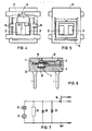
- the infrared detector shown in FIGS. 2 to 6 has two detector elements 17, optionally a bleeder resistor 19, which is supplemented by two antiparallel diodes 20 with leakage currents in the range of pA and an FET 16.
- an infrared detector with the above-mentioned components in a plastic-molded housing with four connection contacts, two of which form the connection contacts “Source” and “Drain” of the FET and the other two provide the ground contact.
- the structure of the infrared detector is based on a contact spider according to FIG. 1.
- a sheet metal strip 4 is bent out of this shaped sheet 3, which is used for contacting and supporting the ground connection of the FET 16.
- another sheet 5 is bent down, which provides a shield under the FET 16.
- the width of this shaped plate 3 is dimensioned such that there are two positioning webs 6 for the FET 16 on both sides.
- Retaining webs 8, which are separated after the extrusion coating, are used for stiffening during assembly. Furthermore, sheets 9, 10 are bent up vertically on three sides, which form the side shield. The sheets 10 also create the connection to the infrared filter 15, which closes the shielding cage.
- the encapsulated FET 16 with integrated diodes 20 is positioned by the pocket formed in the contact spider.
- the source, drain and ground connection is connected for contacting by welding or soldering to the sheet metal strips 4 or sheets 7.
- the gate connection of the FET 16 hangs freely and is used for later contacting the upper detector element 17 (FIG. 7).
- the structure according to FIG. 2 can be extrusion-coated with thermosets or thermoplastics.
- An opening 11 is created in the housing in which the ground and gate contact of the FET 16 are open (see FIG. 2).
- This opening contains a step 12 at the level of the FET contacts, which serves to receive the detector elements 17.
- the wall is tapered towards the bottom, so that the detector elements 17 are automatically positioned after insertion.
- the contact to the ground and gate connection of the FET's 16 is either soldered or conductively glued.
- the resistor 19 can be contacted with pads downward be (see Fig. 6).
- This resistor 19, which acts as a gate bleeder resistor, is applied to an aluminum oxide substrate.
- the resistor 19 is mounted over the FET 16 or on the bottom of the housing opening as shown in FIG.
- the housing opening contains a further circumferential step 13 on the upper edge, which serves to receive the infrared filter 15.
- free spaces 14 are created on the long sides, which form a reservoir for the conductive adhesive when the housing is closed.
- the sheets 10 of the shaped sheet 3 protrude into this step (see FIGS. 3 and 4).
- the holding webs 8 are punched out.
- the connecting pins (earth contacts 1, plates 7) are separated from the holding and positioning strips 2 and bent downwards by 90 °.
- FIG. 8 shows the design of a 4-element detector with two FETs 16 in the same manufacturing technology. Two independently operating dual element detector elements 17a are included. During assembly, a correspondingly modified molded sheet 3a is assumed.
- the housing is formed by a plastic molded part 21, 21a in which a molded sheet 3, 3a and the components 16, 17, 17a, if appropriate 19 and 20, are embedded , wherein the shaped plate 3, 3a electrically connects the components 16, 17, 17a, if necessary 19 and 20, and with outwardly projecting projections, namely the ground contacts 1 and the plates 7, for the electrical connection of the infrared detector is.
- the steps 12, 13, which are visible in particular in FIGS. 2, 3, 6, 8, for receiving the detector elements 17, 17a and the infrared filter 15 are arranged.
- the bent areas, namely the sheet metal strip 4, the sheet metal 5 and the sheets 9, 10 cover the components 16, 17, 17a, if necessary, 19 and 20 for shielding.
Abstract
Description
- Die Erfindung betrifft einen infrarotdetektor mit mindestens einem Detektorelement, das in einem Gehäuse gehaltert ist, welches ein für Infrarotstrahlung durchlässiges Fenster über dem Detektorelement aufweist, und mit weiteren elektrischen Bauelementen, die mit dem Detektorelement zusammengeschaltet sind.
- Infrarotdetektoren dieser Art mit pyroelektrischen Detektorelementen finden ihre Hauptanwendung in Einbruchalarmgeräten und automatischen Lichtschaltern Ausgenutzt wird die in der Regel von der Umgebung unterschiedliche Temperatur des menschlichen Körpers Bewegt sich ein Mensch im Erfassungsbereich eines infrarotdetektors, so ändert sich die auf dem Detektorelement auftreffende Strahlungsleistung und damit die Temperatur des Detektorelementes. Aufgrund des pyroelektrischen Effektes ändert sich dabei die spontane Polarisation des Materials, was zu einer Ladungserzeugung führt. Diese Ladung wird auf Elektroden abgezogen und mittels eines Impedanzwandlers in eine Spannung umgeformt. Als Impedanzwandler dient ein Feldeffekttransistor mit geringem Gate-Leck-Strom.
- Die bisher verfügbaren Infrarotdetektoren für die beschriebene Anwendung verwenden ein für Infrarotstrahlung durchlässiges Fenster, das in eine metallische Gehäusekappe eingeklebt wird. Auf einer Montageplatte werden die Bauelemente montiert und die beiden Gehäuseteile dicht miteinander verbunden.
- Die bekannten Ausführungen von Infrarotdetektoren haben alle den Nachteil, daß eine automatische Prüfung und Positionierung auf einer Leiterplatte nur in sehr eingeschränktem Umfang oder mit aufwendigen Spezialgeräten möglich ist.
- Der Erfindung liegt die Aufgabe zugrunde, einen Infrarotdetek tor der eingangs genannten Art so auszubilden, daß er bei mindestens gleichen optoelektrischen Daten wie bekannte Ausführungen sich durch einfache Montage, höhere Zuverlässigkeit und vereinfachte Weiterverarbeitung auszeichnet.
- Diese Aufgabe ist erfindungsgemäß dadurch gelöst, daß das Gehäuse von einem Kunststoff-Formteil gebildet ist, in dem ein Formblech sowie die Bauelemente eingebettet sind, wobei das Formblech die Bauelemente elektrisch verbindet und mit vom Formteil nach außen ragenden Ansätzen zum elektrischen Anschluß versehen ist, und daß im Formteil Stufen zur Aufnahme des Detektorelementes und eines Infrarotfilters angeordnet sind. Bei dem erfindungsgemäßen Infrarotdetektor ist aufgrund der aus dem Formteil herausragenden Anschlußkontakte eine definierte optische Ausrichtung ohne zusätzliche Justierhilfsmittel gewährleistet. Es kann auf gebräuchliche Montageeinrichtungen zurückgegriffen werden.
- Als pyroelektrisches Material für das Detektorelement wird ein dünnes Plättchen einer Keramik oder eines Kristalles verwendet. Auf der Oberfläche dieses Plättchens sind Elektroden aufgebracht, die zwei getrennte Kondensatoren bilden. Diese sind entweder seriell oder entgegengesetzt parallel verschaltet. Dabei ist für den erfindungsgemäßen Aufbau die serielle Verschaltung empfehlenswert. Bei dieser seriellen Verschaltung sind die Elektroden auf der der Strahlung zugewandten Seite verbunden und eventuell zusätzlich mit einer Infrarotstrahlung absorbierenden Schicht versehen.
- Wie bei in Kunststoff gekapselten elektrischen Bauelementen üb lich, wird beim Aufbau des Infrarotdetektors von einer Kontaktspinne ausgegangen. Diese beinhaltet die Montage- und Kontaktflächen für die Bauteile und enthält die Anschlußkontakte des späteren Infrarotdetektors. Diese Anschlußkontakte sind mit Haltestegen verbunden, um eine Abarbeitung von einer Endlosrolle zu ermöglichen. Wegen der hohen Impedanz der Detektorelemente ist es notwendig, eine möglichst vollständige leit fähige Umschließung dieser Detektorelemente und auch des Feldeffekttransistors (FET) zu erreichen. Daher wurden bisher fast ausschließlich Metallgehäuse verwendet. Teile des Formbleches sind bei der vorliegenden Erfindung nach oben gebogen und bilden damit zusammen mit der Grundfläche einen Teil des Abschirmkäfigs. Ein aus Abschirmmaterial bestehendes Gehäuse kann demgemäß entfallen. Als Impedanzwandler kann ein gekapselter FET verwendet werden.
- Die Anschlüsse des Formbleches für Source-, Drain- und Masseverbindung zum FET sind in verschiedene Ebenen gebogen und so geformt, daß sie zusammen mit dem Formblech eine Tasche bilden, in der der FET positioniert werden kann. Dies ermöglicht eine einfache Montage.
- Beim Einspritzen mit Duro- oder Thermoplasten wird eine Öffnung im Gehäuse belassen, durch die das gegen hohe Temperaturen empfindliche Sensorelement nachträglich montiert wird. Dabei sind Auflage- und Positionierflächen am Formblech und an der Umspritzung, also am Formteil, ausgebildet. Zusätzlich enthält das Formteil um seine Öffnung herum einen Aufnahmerand, in den das Infrarotfenster in Form eines Fensters eingeklebt wird.
- Das Formblech ist weiterhin so geformt, daß hochstehende Flächen beim Einkleben des Infrarotfilters mit diesem leitfähig verbunden werden und damit den Abschirmkäfig schließen.
- Durch den beschriebenen Aufbau wird eine automatische Montage auf Fertigungsanlagen ermöglicht, wie sie sich in der Halbleiter-Chipkonfektionierung schon lange bewährt hat.
- In der gleichen Bauform ist es durch Hinzunahme von weiteren Anschlüssen und damit Verlängern des Gehäuses möglich, die für die Anwendung des Infrarotdetektors in einem Alarmgerät oder in einem automatischen Lichtschalter notwendigen Schaltelemente zu integrieren.
- Die Erfindung ist nachfolgend anhand von in der Zeichnung dargestellten Ausführungsbeispielen näher erläutert. Es zeigen:
- Fig. 1 eine Kontaktspinne zur Erläuterung der Fertigung des erfindungsgemäßen Infrarotdetektors,
- Fig. 2 und 3 zwei zueinander senkrecht liegende Schnitte durch einen Infrarotdetektor nach der Erfindung,
- Fig. 4 und 5 eine Aufsicht von innen und von außen des Infrarotdetektors gemäß den Fig. 2 und 3,
- Fig. 6 einen Schnitt durch eine Variante des Infrarotdetektors gemäß den Fig. 2 bis 5,
- Fig. 7 das Schaltbild des Infrarotdetektors gemäß den Fig. 1 bis 6, und
- Fig. 8 eine weitere Variante eines Infrarotdetektors nach der Erfindung im Schnitt.
- Der in den Fig. 2 bis 6 dargestellte Infrarotdetektor weist gemäß Fig. 7 zwei Detektorelemente 17, gegebenenfalls einen Ableitwiderstand 19, der durch zwei antiparallele Dioden 20 mit Leckströmen im Bereich von pA ergänzt wird und einen FET 16 auf.
- In den Fig. 2 bis 6 ist ein Infrarotdetektor mit den genannten Bauteilen in einem kunstoffgespritzten Gehäuse mit vier Anschlußkontakten, wovon zwei die Anschlußkontakte "Source" und "Drain" des FET's bilden und die beiden weiteren den Massekontakt liefern, beschrieben.
- Der Aufbau des Infrarotdetektors geht von einer Kontaktspinne nach Fig. 1 aus. Die Massekontakte 1, die nach beiden Seiten mit einem Halte- und Positionierstreifen 2 verbunden sind, halten und kontaktieren ein Formblech 3 der gleichen Kontakt spinne. Aus diesem Formblech 3 ist nach oben ein Blechstreifen 4 herausgebogen, der zur Kontaktierung und Stützung des Masseanschlusses des FET's 16 dient. Zusätzlich ist ein weiteres Blech 5 heruntergebogen, das unter dem FET 16 für eine Abschirmung sorgt. Die Breite dieses Formbleches 3 ist so bemessen, daß sich auf beiden Seiten zwei Positionierstege 6 für den FET 16 ergeben.
- Zum Anschluß von "Source" und "Drain" dienen zwei auf die Höhe der Massekontakte 1 gebogene Bleche 7.
- Zur Versteifung während der Montage dienen Haltestege 8, die nach dem Umspritzen abgetrennt werden. Weiterhin sind auf drei Seiten Bleche 9, 10 senkrecht hochgebogen, die die seitliche Abschirmung bilden. Die Bleche 10 schaffen auch die Verbindung zum Infrarotfilter 15, der den Abschirmkäfig schließt.
- Der gekapselte FET 16 mit integrierten Dioden 20 wird von der in der Kontaktspinne gebildeten Tasche positioniert. Der Source-, Drain- und Masseanschluß wird zur Kontaktierung durch Verschweißen oder Verlöten mit den Blechstreifen 4 bzw. Blechen 7 verbunden. Der Gateanschluß des FET 16 hängt dabei frei und dient zur späteren Kontaktierung des oberen Detektorelementes 17 (Fig. 7).
- Nach der Montage des FET's 16 kann der Aufbau gemäß Fig. 2 bis im Vielfachwerkzeug mit Duro- oder Thermoplasten umspritzt werden. Dabei wird im Gehäuse eine Öffnung 11 geschaffen, in der der Masse- und Gatekontakt des FET 16 offen liegen (siehe Fig. 2). Diese Öffnung enthält in Höhe der FET-Kontakte eine Stufe 12, die zur Aufnahme der Detektorelemente 17 dient. Die Wandung ist nach unten hin schräg zulaufend ausgeführt, so daß die Detektorelemente 17 nach Einbringen automatisch positioniert werden. Der Kontakt zu dem Masse- und Gateanschluß des FET's 16 wird entweder gelötet oder leitfähig verklebt. Zusätzlich kann auf den Masse- und Gateanschlußkontakt des FET's 16 der Widerstand 19 mit Anschlußflächen nach unten kontaktiert werden (siehe Fig. 6). Dieser als Gateableitwiderstand wirkende Widerstand 19 ist auf einem Aluminiumoxydsubstrat aufgebracht. Der Widerstand 19 wird wie in Fig. 6 gezeigt über dem FET 16 oder auf dem Boden der Gehäuseöffnung montiert und in diesem Fall mit Anschlußkontakten nach oben mit dem Masse- und Gateanschluß des FET's 16 verbunden.
- Die Gehäuseöffnung enthält am oberen Rand eine weitere umlaufende Stufe 13, die zur Aufnahme des Infrarotfilters 15 dient. Dabei sind auf den Längsseiten Freiräume 14 geschaffen, die ein Reservoir für den leitfähigen Kleber beim Verschließen des Gehäuses bilden. In diese Stufe ragen die Bleche 10 des Formbleches 3 hinein (siehe Fig. 3 und 4).
- Zur Entgasung beim Aushärten des Klebers dient eine kleine Öffnung 18 auf der Gehäuseunterseite, die anschließend verschlossen wird.
- Nach Abdichten des vorher mit Stickstoff gefluteten Gehäuses werden die Haltestege 8 abgestanzt. Die Anschlußbeinchen (Massekontakte 1, Bleche 7) werden von den Halte- und Positionierstreifen 2 getrennt und um 90° nach unten gebogen.
- Die Fig. 8 zeigt die Ausführung eines 4-Element-Detektors mit zwei FET's 16 in gleicher Fertigungstechnik. Dabei sind zwei unabhängig arbeitende Dual-Element-Detektorelemente 17a enthalten. Bei der Montage wird von einem entsprechend geänderten Formblech 3a ausgegangen.
- Gemeinsam ist den in den Fig. 2 bis 6, 8 gezeigten Ausführungsbeispielen, daß das Gehäuse von einem Kunststoff-Formteil 21, 21a gebildet ist, in dem ein Formblech 3, 3a sowie die Bauelemente 16, 17, 17a gegebenenfalls 19 und 20 eingebettet sind, wobei das Formblech 3, 3a die Bauelemente 16, 17, 17a gegebenenfalls 19 und 20 elektrisch verbindet und mit nach außen ragenden Ansätzen, nämlich den Massekontakten 1 und den Blechen 7, zum elektrischen Anschluß des Infrarotdetektors versehen ist. Im Formteil 21, 21a sind die insbesondere in den Fig. 2, 3, 6, 8 sichtbaren Stufen 12, 13 zur Aufnahme der Detektorelemente 17, 17a und des Infrarotfilters 15 angeordnet. Die abgebogenen Bereiche, nämlich der Blechstreifen 4, das Blech 5 und die Bleche 9, 10 decken die Bauelemente 16, 17, 17a gegebenenfalls 19 und 20 zur Abschirmung ab.
Claims (2)
Applications Claiming Priority (4)
| Application Number | Priority Date | Filing Date | Title |
|---|---|---|---|
| DE8808109 | 1988-06-23 | ||
| DE8808109U | 1988-06-23 | ||
| DE8808815U DE8808815U1 (de) | 1988-06-23 | 1988-07-08 | |
| DE8808815U | 1988-07-08 |
Publications (2)
| Publication Number | Publication Date |
|---|---|
| EP0347704A1 true EP0347704A1 (de) | 1989-12-27 |
| EP0347704B1 EP0347704B1 (de) | 1993-12-15 |
Family
ID=25953204
Family Applications (1)
| Application Number | Title | Priority Date | Filing Date |
|---|---|---|---|
| EP89110605A Expired - Lifetime EP0347704B1 (de) | 1988-06-23 | 1989-06-12 | Infrarotdetektor |
Country Status (4)
| Country | Link |
|---|---|
| US (1) | US4967081A (de) |
| EP (1) | EP0347704B1 (de) |
| JP (1) | JPH081458Y2 (de) |
| DE (2) | DE8808815U1 (de) |
Cited By (3)
| Publication number | Priority date | Publication date | Assignee | Title |
|---|---|---|---|---|
| DE4214792A1 (de) * | 1992-05-04 | 1993-11-11 | Telefunken Microelectron | Verfahren zum Herstellen eines optoelektronischen Koppelelements |
| EP0588073A1 (de) * | 1992-08-14 | 1994-03-23 | Cerberus Ag | Pyroelektrischer Sensor für passive Infrarotbewegungsdetektoren |
| DE19637946A1 (de) * | 1995-09-18 | 1997-03-20 | Murata Manufacturing Co | Infrarotsensor, Sensorherstellungspalette und Verfahren zur Herstellung eines Infrarotsensors |
Families Citing this family (20)
| Publication number | Priority date | Publication date | Assignee | Title |
|---|---|---|---|---|
| US5239296A (en) * | 1991-10-23 | 1993-08-24 | Black Box Technologies | Method and apparatus for receiving optical signals used to determine vehicle velocity |
| DE4212948A1 (de) * | 1992-04-18 | 1993-10-21 | Telefunken Microelectron | Halbleiterbaugruppe, insbesondere Fernsteuer-Empfangsmodul |
| KR940001333A (ko) * | 1992-06-16 | 1994-01-11 | 문정환 | 수지봉합형 고체촬상소자 패키지 및 그 제조방법 |
| EP0866955A4 (de) * | 1995-12-07 | 2000-09-20 | Diasense Inc | Eine vielzahl photoleitender detektoren in einer kompakten verpackung zusammenfassende matrixanordnung |
| US5962909A (en) * | 1996-09-12 | 1999-10-05 | Institut National D'optique | Microstructure suspended by a microsupport |
| US5831266A (en) * | 1996-09-12 | 1998-11-03 | Institut National D'optique | Microbridge structure for emitting or detecting radiations and method for forming such microbridge structure |
| US6252220B1 (en) | 1999-04-26 | 2001-06-26 | Xerox Corporation | Sensor cover glass with infrared filter |
| US6768565B1 (en) | 2000-09-07 | 2004-07-27 | Xerox Corporation | Infrared correction in color scanners |
| US6316284B1 (en) | 2000-09-07 | 2001-11-13 | Xerox Corporation | Infrared correction in color scanners |
| DE10102119C1 (de) * | 2001-01-18 | 2002-04-04 | Vishay Semiconductor Gmbh | Optoelektronisches Bauelement mit Leiterstreifenaufbau und Verfahren zu seiner Herstellung |
| US6937152B2 (en) * | 2003-04-08 | 2005-08-30 | Shoot The Moon Products Ii, Llc | Wireless interactive doll-houses and playsets therefor |
| DE10327694A1 (de) * | 2003-06-20 | 2005-01-05 | Robert Bosch Gmbh | Optische Sensoranordnung und entsprechendes Herstellungsverfahren |
| ITMI20050334A1 (it) * | 2004-03-11 | 2005-09-12 | Leuze Electronic Gmbh Co Kg | Sensore ottico per il rilevamento di oggetti in una zona di monitoraggio |
| US7514672B2 (en) * | 2005-02-15 | 2009-04-07 | Sumitomo Chemical Company, Limited | Case for accommodating solid-state imaging device and solid-state imaging apparatus |
| US9473681B2 (en) * | 2011-06-10 | 2016-10-18 | Flir Systems, Inc. | Infrared camera system housing with metalized surface |
| JP5706217B2 (ja) * | 2011-03-31 | 2015-04-22 | 旭化成エレクトロニクス株式会社 | 赤外線センサ |
| JP5798952B2 (ja) * | 2012-03-06 | 2015-10-21 | 旭化成エレクトロニクス株式会社 | 赤外線検出装置 |
| JP6097496B2 (ja) * | 2012-06-21 | 2017-03-15 | 旭化成エレクトロニクス株式会社 | 赤外線センサの製造方法 |
| US10996542B2 (en) | 2012-12-31 | 2021-05-04 | Flir Systems, Inc. | Infrared imaging system shutter assembly with integrated thermister |
| JP6039789B2 (ja) | 2013-02-14 | 2016-12-07 | 旭化成エレクトロニクス株式会社 | 赤外線センサ及びその製造方法 |
Citations (5)
| Publication number | Priority date | Publication date | Assignee | Title |
|---|---|---|---|---|
| US4047045A (en) * | 1975-03-03 | 1977-09-06 | Paxton Jr Grady W | Optical coupler |
| DE2916744A1 (de) * | 1978-04-26 | 1979-10-31 | Murata Manufacturing Co | Detektor fuer infrarotstrahlung und verfahren zu dessen herstellung |
| US4198564A (en) * | 1977-04-19 | 1980-04-15 | U.S. Philips Corporation | Pyroelectric detector circuits and devices |
| DE2950649A1 (de) * | 1978-12-19 | 1980-06-26 | Tokyo Shibaura Electric Co | Fotoelektrische kopplungsvorrichtung |
| GB2107929A (en) * | 1981-10-14 | 1983-05-05 | Gen Electric | Optocouplers |
Family Cites Families (5)
| Publication number | Priority date | Publication date | Assignee | Title |
|---|---|---|---|---|
| JPS59596Y2 (ja) * | 1975-03-14 | 1984-01-09 | 株式会社ニコン | ロシウツケイノジユコウキ |
| JPS584953A (ja) * | 1981-07-01 | 1983-01-12 | Toshiba Corp | 半導体装置 |
| US4650998A (en) * | 1984-12-10 | 1987-03-17 | Siemens Corporate Research & Support, Inc. | Highly aligned optical device |
| EP0184747A1 (de) * | 1984-12-13 | 1986-06-18 | Heimann GmbH | Infrarotdetektor |
| ATE45230T1 (de) * | 1985-01-10 | 1989-08-15 | Teletronic Hartmuth Jensen | Sensor fuer ueberwachungsanlagen. |
-
1988
- 1988-07-08 DE DE8808815U patent/DE8808815U1/de not_active Expired
-
1989
- 1989-06-12 DE DE89110605T patent/DE58906411D1/de not_active Expired - Fee Related
- 1989-06-12 EP EP89110605A patent/EP0347704B1/de not_active Expired - Lifetime
- 1989-06-15 US US07/366,613 patent/US4967081A/en not_active Expired - Lifetime
- 1989-06-16 JP JP1989070729U patent/JPH081458Y2/ja not_active Expired - Lifetime
Patent Citations (5)
| Publication number | Priority date | Publication date | Assignee | Title |
|---|---|---|---|---|
| US4047045A (en) * | 1975-03-03 | 1977-09-06 | Paxton Jr Grady W | Optical coupler |
| US4198564A (en) * | 1977-04-19 | 1980-04-15 | U.S. Philips Corporation | Pyroelectric detector circuits and devices |
| DE2916744A1 (de) * | 1978-04-26 | 1979-10-31 | Murata Manufacturing Co | Detektor fuer infrarotstrahlung und verfahren zu dessen herstellung |
| DE2950649A1 (de) * | 1978-12-19 | 1980-06-26 | Tokyo Shibaura Electric Co | Fotoelektrische kopplungsvorrichtung |
| GB2107929A (en) * | 1981-10-14 | 1983-05-05 | Gen Electric | Optocouplers |
Non-Patent Citations (1)
| Title |
|---|
| PATENT ABSTRACTS OF JAPAN, Band 7, Nr. 76 (E-167)[1221], 30. März 1983, Seite 72 E 167; & JP-A-58 004 953 (TOKYO SHIBAURA DENKI K.K.) 12-01-1983 * |
Cited By (5)
| Publication number | Priority date | Publication date | Assignee | Title |
|---|---|---|---|---|
| DE4214792A1 (de) * | 1992-05-04 | 1993-11-11 | Telefunken Microelectron | Verfahren zum Herstellen eines optoelektronischen Koppelelements |
| US5299727A (en) * | 1992-05-04 | 1994-04-05 | Temic Telefunken Microelectronic Gmbh | Method of manufacture of an optoelectronic coupling element |
| EP0588073A1 (de) * | 1992-08-14 | 1994-03-23 | Cerberus Ag | Pyroelektrischer Sensor für passive Infrarotbewegungsdetektoren |
| DE19637946A1 (de) * | 1995-09-18 | 1997-03-20 | Murata Manufacturing Co | Infrarotsensor, Sensorherstellungspalette und Verfahren zur Herstellung eines Infrarotsensors |
| DE19637946C2 (de) * | 1995-09-18 | 2001-06-28 | Murata Manufacturing Co | Verfahren zum Befestigen eines Infrarotfilters an einem Gehäuse und Vorrichtung zum Durchführen des Verfahrens |
Also Published As
| Publication number | Publication date |
|---|---|
| JPH081458Y2 (ja) | 1996-01-17 |
| JPH0310224U (de) | 1991-01-31 |
| US4967081A (en) | 1990-10-30 |
| DE58906411D1 (de) | 1994-01-27 |
| DE8808815U1 (de) | 1988-09-15 |
| EP0347704B1 (de) | 1993-12-15 |
Similar Documents
| Publication | Publication Date | Title |
|---|---|---|
| EP0347704B1 (de) | Infrarotdetektor | |
| DE112005000446B4 (de) | Paket mit piezoelektrischem Resonatorelement und piezoelektrischer Resonator | |
| DE3118298C2 (de) | ||
| DE2020925A1 (de) | Mikrowellen-Baugruppe | |
| EP2038624B1 (de) | Elektrisches bauelement mit einem sensorelement und verfahren zur verkapselung eines sensorelements | |
| DE2642842C2 (de) | Elektronischer Rechner | |
| DE4235185A1 (de) | Flache leistungsversorgungseinheit | |
| DE3832991A1 (de) | Zellstruktur fuer matrix-adressierte fluessigkristallanzeigen und verfahren zu deren herstellung | |
| DE2140107A1 (de) | Fotodetektoranordnung | |
| DE2903838C2 (de) | Elektrooptisches Lichtmodulationselement | |
| DE19923960A1 (de) | Infrarotsensor | |
| DE1912045A1 (de) | Halterungsanordnung fuer ein Halbleiterbauelement | |
| DE3913066C2 (de) | ||
| DE19846254A1 (de) | Infrarotsensor | |
| DE19730140C2 (de) | Variabler Kondensator und zusammengesetzte LC-Module unter Verwendung desselben | |
| EP0216136B1 (de) | Sensorelementeanordnung in einem Halterahmen für einen Pyrodetektor und Verfahren zu deren Herstellung | |
| EP0218056A1 (de) | Pyrodetektor zur Detektion eines in seinen Detektionsbereich eintretenden Körpers | |
| DE10005678A1 (de) | Elektrochromes Abblendsystem | |
| DE10003501A1 (de) | Elektronische Bauteilvorrichtung | |
| DE3637988A1 (de) | Anzuendbauteil | |
| DE4438673A1 (de) | Pyroelektrischer Infrarot-Array-Sensor | |
| EP0400193B1 (de) | Sensoreinrichtung | |
| DE3131887A1 (de) | Elektrisches bauelement, bauelementegruppe oder integrierte schaltung, deren aktiver teil auf einem metalltraeger aufgebacht ist, und verfahren zu ihrer herstellung | |
| DE6607827U (de) | Halbleiterbauteil | |
| EP0763895A2 (de) | Schaltungsanordnung und Halbleiterkörper mit einem Leistungsschalter |
Legal Events
| Date | Code | Title | Description |
|---|---|---|---|
| PUAI | Public reference made under article 153(3) epc to a published international application that has entered the european phase |
Free format text: ORIGINAL CODE: 0009012 |
|
| AK | Designated contracting states |
Kind code of ref document: A1 Designated state(s): DE FR GB NL |
|
| 17P | Request for examination filed |
Effective date: 19900126 |
|
| RAP1 | Party data changed (applicant data changed or rights of an application transferred) |
Owner name: HEIMANN OPTOELECTRONICS GMBH |
|
| 17Q | First examination report despatched |
Effective date: 19930204 |
|
| GRAA | (expected) grant |
Free format text: ORIGINAL CODE: 0009210 |
|
| AK | Designated contracting states |
Kind code of ref document: B1 Designated state(s): DE GB |
|
| GBT | Gb: translation of ep patent filed (gb section 77(6)(a)/1977) |
Effective date: 19931220 |
|
| REF | Corresponds to: |
Ref document number: 58906411 Country of ref document: DE Date of ref document: 19940127 |
|
| EN | Fr: translation not filed | ||
| PLBE | No opposition filed within time limit |
Free format text: ORIGINAL CODE: 0009261 |
|
| STAA | Information on the status of an ep patent application or granted ep patent |
Free format text: STATUS: NO OPPOSITION FILED WITHIN TIME LIMIT |
|
| 26N | No opposition filed | ||
| REG | Reference to a national code |
Ref country code: GB Ref legal event code: IF02 |
|
| PGFP | Annual fee paid to national office [announced via postgrant information from national office to epo] |
Ref country code: GB Payment date: 20050531 Year of fee payment: 17 |
|
| PGFP | Annual fee paid to national office [announced via postgrant information from national office to epo] |
Ref country code: DE Payment date: 20050829 Year of fee payment: 17 |
|
| PG25 | Lapsed in a contracting state [announced via postgrant information from national office to epo] |
Ref country code: GB Free format text: LAPSE BECAUSE OF NON-PAYMENT OF DUE FEES Effective date: 20060612 |
|
| PG25 | Lapsed in a contracting state [announced via postgrant information from national office to epo] |
Ref country code: DE Free format text: LAPSE BECAUSE OF NON-PAYMENT OF DUE FEES Effective date: 20070103 |
|
| GBPC | Gb: european patent ceased through non-payment of renewal fee |
Effective date: 20060612 |