EP0347083B1 - Konfiguration für TTL-Ausgangstreibergatter - Google Patents
Konfiguration für TTL-Ausgangstreibergatter Download PDFInfo
- Publication number
- EP0347083B1 EP0347083B1 EP89305653A EP89305653A EP0347083B1 EP 0347083 B1 EP0347083 B1 EP 0347083B1 EP 89305653 A EP89305653 A EP 89305653A EP 89305653 A EP89305653 A EP 89305653A EP 0347083 B1 EP0347083 B1 EP 0347083B1
- Authority
- EP
- European Patent Office
- Prior art keywords
- gate
- pull
- transistor
- node
- output
- Prior art date
- Legal status (The legal status is an assumption and is not a legal conclusion. Google has not performed a legal analysis and makes no representation as to the accuracy of the status listed.)
- Expired - Lifetime
Links
- WYTGDNHDOZPMIW-RCBQFDQVSA-N alstonine Natural products C1=CC2=C3C=CC=CC3=NC2=C2N1C[C@H]1[C@H](C)OC=C(C(=O)OC)[C@H]1C2 WYTGDNHDOZPMIW-RCBQFDQVSA-N 0.000 claims abstract description 24
- 230000007704 transition Effects 0.000 claims abstract description 21
- 229910021420 polycrystalline silicon Inorganic materials 0.000 abstract description 6
- 229920005591 polysilicon Polymers 0.000 abstract description 6
- 239000000463 material Substances 0.000 abstract description 3
- 230000009467 reduction Effects 0.000 abstract description 2
- 239000000872 buffer Substances 0.000 description 11
- 230000008859 change Effects 0.000 description 3
- 230000001939 inductive effect Effects 0.000 description 3
- 230000004044 response Effects 0.000 description 3
- 230000000295 complement effect Effects 0.000 description 2
- 238000010586 diagram Methods 0.000 description 2
- 238000007599 discharging Methods 0.000 description 2
- 230000000694 effects Effects 0.000 description 2
- 230000003071 parasitic effect Effects 0.000 description 2
- 230000000644 propagated effect Effects 0.000 description 2
- 230000001052 transient effect Effects 0.000 description 2
- 230000001419 dependent effect Effects 0.000 description 1
- 230000005669 field effect Effects 0.000 description 1
- 238000012986 modification Methods 0.000 description 1
- 230000004048 modification Effects 0.000 description 1
- 238000004806 packaging method and process Methods 0.000 description 1
- 230000002093 peripheral effect Effects 0.000 description 1
- 239000004065 semiconductor Substances 0.000 description 1
Images
Classifications
-
- H—ELECTRICITY
- H03—ELECTRONIC CIRCUITRY
- H03K—PULSE TECHNIQUE
- H03K19/00—Logic circuits, i.e. having at least two inputs acting on one output; Inverting circuits
- H03K19/02—Logic circuits, i.e. having at least two inputs acting on one output; Inverting circuits using specified components
- H03K19/08—Logic circuits, i.e. having at least two inputs acting on one output; Inverting circuits using specified components using semiconductor devices
- H03K19/094—Logic circuits, i.e. having at least two inputs acting on one output; Inverting circuits using specified components using semiconductor devices using field-effect transistors
- H03K19/0944—Logic circuits, i.e. having at least two inputs acting on one output; Inverting circuits using specified components using semiconductor devices using field-effect transistors using MOSFET or insulated gate field-effect transistors, i.e. IGFET
- H03K19/0948—Logic circuits, i.e. having at least two inputs acting on one output; Inverting circuits using specified components using semiconductor devices using field-effect transistors using MOSFET or insulated gate field-effect transistors, i.e. IGFET using CMOS or complementary insulated gate field-effect transistors
-
- H—ELECTRICITY
- H03—ELECTRONIC CIRCUITRY
- H03K—PULSE TECHNIQUE
- H03K19/00—Logic circuits, i.e. having at least two inputs acting on one output; Inverting circuits
- H03K19/003—Modifications for increasing the reliability for protection
- H03K19/00346—Modifications for eliminating interference or parasitic voltages or currents
- H03K19/00361—Modifications for eliminating interference or parasitic voltages or currents in field effect transistor circuits
Definitions
- This invention relates generally to CMOS integrated circuits and more particularly, it relates to a TTL output driver gate configuration which has reduced voltage spikes on internal power supply potential and ground potential nodes.
- CMOS complementary metal-oxide-semiconductor
- TTL transistor-transistor-logic
- Output buffer circuits typically use a pull-up transistor device and a pull-down transistor device connected in series between first and second power supply terminals.
- the first power supply terminal may be supplied with a positive potential +V, which is connected to an internal power supply potential node.
- a second power supply terminal may be supplied with a negative potential -V or a ground potential, which is connected to an internal ground potential node.
- the connection point of the pull-up and pull-down transistor devices is further joined to an output terminal or pad.
- either the pull-up or pull-down transistor device Dependent upon the logic state of the data input signal and an enable signal, either the pull-up or pull-down transistor device is quickly turned ON and the other one of them is turned OFF.
- Such rapid switching ON and OFF of the pull-up and pull-down transistor devices causes sudden surges of current (di/dt or current spikes) in the power supply and ground lines due to parasitic packaging and interconnect inductance and resistance.
- charging and discharging currents from the pull-up and pull-down transistors driving large capacitive loads exists.
- These transient currents current surges and charging/discharging currents
- United States Patent Specification No. 4,725,747 discloses an arrangement of a complementary pair of P-channel and N-channel output transistors. These output transistors are formed with gate structures which are serpentine to provide a gradual or graded turn on characteristic.
- the output driver gate configuration of the present invention includes a pull-up transistor and a pull-down transistor whose gates are made serpentine and are driven at only end thereof.
- the reduction of voltage spikes is achieved by slowing down the turn-on times of the pull-up and pull-down transistors during transitions by means of the distributed resistances and capacitances of the polysilicon material used to form the gates thereof.
- an output driver gate arranged to drive TTL logic comprising: a P-channel pull-up transistor (P1) having a serpentine gate, a source and a drain, said source being arranged to be coupled to a positive supply potential (V+) via an internal power supply potential node (F), said drain being coupled to an output node (G), and said serpentine gate of said pull-up transistor (P1) having respective first and second ends; an N-channel pull-down transistor (N1) having a serpentine gate, a source and a drain, said source being arranged to be coupled to a negative or ground supply potential (V-) via an internal ground potential node (J), its drain being coupled to said output node (G), said serpentine gate of said pull-down transistor (N1) having respective first and second ends; first logic means (14) arranged to be responsive to a data input signal (DATA) making a low-to-high transition to generate a first control signal which is applied to the gate of said pull-up transistor (P1); and second logic means (16)
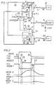
- FIG. 1 a schematic circuit diagram of a TTL output driver gate configuration 10 of the present invention.
- the gate configuration 10 is formed of P-channel pull-up field-effect transistor (FET) P1 and an N-channel pull-down FET N1.
- FET field-effect transistor
- Each of the transistors P1 and N1 is formed with a serpentine gate which is made of a polysilicon material.
- the polysilicon gate provides a distributed combination of resistances and capacitances which facilitates the slowing down of the turn-on times of the transistors as will be more fully explained hereinafter.
- the gate configuration 10 provides an output signal at an output node A in response to a data input signal DATA received at a data input node B and an enable signal EN received at an enable input node C.
- the gate configuration 10 further includes an inverter 12, a NAND logic gate 14, a NOR logic gate 16, a first positive feedback amplifier circuit 18, and a second positive feedback amplifier circuit 20.
- Power for all of the components of the gate configuration 10 is provided by first external and second external power supply terminals 21, 23.
- a positive supply voltage or potential +V is applied to the first power supply terminal 21, and a negative power supply voltage or potential -V or ground potential is applied at the second power supply terminal 23.
- the positive supply voltage +V is made to be approximately +5.0 volts.
- the negative power supply voltage -V is made to be zero volts.
- the gate configuration 10 is used to drive the output node A, which has a capacitive load CAP connected thereto, through a line 22 having parasitic inductance L.
- the NAND logic gate 14 receives the data input signal DATA on line 24 on its one input and the enable signal EN on line 26 via the inverter 12 on its other input.
- the output of the NAND logic gate 14 on line 28 is applied to a node D defining the driven end of the serpentine gate of the transistor P1.
- the opposite or undriven end of the serpentine gate of the transistor P1 is defined by node E.
- the transistor P1 has its source connected to an internal power supply potential node F and its drain connected to a common node G.
- the internal power supply potential node F is connected to the first external power supply terminal 21 via a series-connected resistor R1 and inductor L1, which represent the resistive and inductive components in the power supply line.
- the NOR logic gate 16 receives the same data input signal DATA on the line 24 on its one input and the same enable signal EN on the line 26 on its other input.
- the output of the NOR logic gate 16 on line 30 is supplied to a node H defining the driven end of the serpentine gate of the transistor N1.
- the opposite or undriven end of the serpentine gate of the transistor N1 is defined by a node I.
- the transistor N1 has its source connected to an internal ground potential node J and its drain connected to the common node G.
- the internal ground potential node J is connected to the second external power supply terminal via a series-connected resistor R2 and inductor L2, which represent the resistive and inductive components in the ground line.
- the first feedback amplifier circuit 18 is formed of a NOR logic gate 32 and an N-channel transistor N2.
- the NOR logic gate 32 has its one input connected to the output of the NAND logic gate 14 on the line 28 (node D) and its other input connected to the node E or undriven end of the P-channel serpentine gate.
- the output of line 34 of the NOR logic gate 32 is connected to the gate of the N-channel transistor N2.
- the transistor N2 has its source connected to the internal ground potential node J and its drain connected to the node E.
- the second feedback amplifier circuit 20 is formed of a NAND logic gate 36 and a P-channel transistor P2.
- the NAND logic gate 36 has its one input connected to the output of the NOR logic gate 16 on the line 30 (node H) and its other input connected to the node I or undriven end of the N-channel serpentine gate.
- the output on line 38 of the NAND logic gate 36 is connected to the gate of the P-channel transistor P2.
- the transistor P2 has its source connected to the internal power supply potential node F and its drain connected to the node I.
- the enable signal EN When the enable signal EN is at the high or logic "1" level, the output of the inverter 12 will be at the low or logic "0" level causing the output of the NAND logic gate 14 to be at the high logic level. As a result, the pull-up transistor P1 will be turned off. Further, the output of the NOR logic gate 16 will be at a low logic level which turns off also the pull-down transistor N1. This produces a high impedance tri-state mode at the common node G in which the gate configuration 10 is not enabled. Thus, for normal operation the enable signal EN must be at a low or logic "0" level.
- the output of the NOR logic gate 16 on the line 30 will quickly make a high-to-low transition so as to turn off the driven gate end of the transistor N1.
- the output of the NAND logic gate 36 on the line 38 will quickly make a low-to-high transition so as to turn off the transistor P2 in response to the change at the output of the NOR gate 16. This in turn causes the undriven end (node I) of the pull-down transistor N1 to be turned off.
- the output of the NAND logic gate 14 on the line 28 defining a control signal will quickly make a high-to-low transition so as to turn on the driven gate end (node D) of the pull-down transistor P1.
- the pull-up transistor P1 will be slowed down in its turn-on time which reduces the current spikes (di/dt) appearing at the internal power supply potential node F.
- the waveform at the node F is illustrated in Figure 2(e).
- the node E will still be at the high logic level and thus, the output of the NOR logic gate 32 will be maintained at the low logic level.
- the waveform at the node E is shown in Figure 2(b).
- the low level at the node D will have propagated through the R-C delay of the serpentine gate and will reach the undriven gate end at the node E, which has the effect of pulling down the node E to about one-half down to the negative supply potential -V.
- the output of the NOR logic gate 32 will make a low-to-high transition so as to cause the transistor N2 to turn on.
- the output of the NAND logic gate 14 on the line 28 will quickly make a low-to-high transition so as to turn off the undriven gate end of the transistor P1.
- the output of the NOR logic gate 32 on the line 34 will quickly make a high-to-low transition so as to turn off the transistor N2. This in turn causes the undriven gate end (node E) of the transistor P1 to be turned off.
- the output of the NOR logic gate 16 will quickly make a low-to-high transition so as to turn on the driven gate end (node H) of the pull-down transistor N1.
- the pull-down transistor N1 will be slowed down in its turn-on time which reduces the current spikes (di/dt) appearing at the internal ground node J, as is illustrated in Figure 2(f).
- the node I will still be at the low logic level and thus the output of the NAND logic gate 36 will be maintained at the high logic level.
- the high level at the node H will have propagated through the R-C delay of the serpentine gate and reach the undriven gate end at the node I, which has the effect of pulling up the node I to about one-half of the positive supply potential +V.
- the output of the NAND logic gate 36 will make a high-to-low transition so as to cause the transistor P2 to turn on.
Landscapes
- Engineering & Computer Science (AREA)
- Physics & Mathematics (AREA)
- Computer Hardware Design (AREA)
- Computing Systems (AREA)
- General Engineering & Computer Science (AREA)
- Mathematical Physics (AREA)
- Power Engineering (AREA)
- Logic Circuits (AREA)
- Electronic Switches (AREA)
- Metal-Oxide And Bipolar Metal-Oxide Semiconductor Integrated Circuits (AREA)
- Power Conversion In General (AREA)
Claims (5)
- Zum Treiben einer TTL-Logik ausgebildetes Ausgangstreibergatter mit:
einem p-Kanal-Pull-up-Transistor (P1) mit einem serpentinenartigen Gate, einer Source und einem Drain, wobei die Source zur Kopplung mit einem positiven Versorgungspotential (V+) über einen internen Energieversorgungspotentialschaltungspunkt (F) ausgebildet ist, das Drain mit einem Ausgangsschaltungspunkt (G) gekoppelt ist und das serpentinenartige Gate des Pull-up-Transistors (P1) erste und zweite Enden aufweist;
einem n-Kanal-Pull-down-Transistor (N1) mit einem serpentinenartigen Gate, einer Source und einem Drain, wobei die Source zur Kopplung mit einem negativen oder Masseversorgungspotential (V-) über einen internen Massepotentialschaltungspunkt (J) ausgebildet ist, sein Drain mit dem Ausgangsschaltungspunkt (G) gekoppelt ist und das serpentinenartige Gate des Pull-down-Transistors (N1) erste und zweite Enden aufweist;
einer ersten Logikeinrichtung (14), die zur Reaktion auf ein einen Low-to-High-Übergang vollziehendes Dateneingangssignal (DATA) ausgebildet ist, um ein erstes Steuersignal zu erzeugen, das an das Gate des Pull-up-Transistors (P1) angelegt wird; und
einer zweiten Logikeinrichtung (16), die zur Reaktion auf das einen High-to-Low-Übergang vollziehendes Dateneingangssignal (DATA) ausgebildet ist, um ein zweites Steuersignal zu erzeugen, das an das Gate des Pull-down-Transistors (N1) angelegt wird;
gekennzeichnet
dadurch, daß das erste Steuersignal an das erste Ende des Gates des Pull-up-Transistors (P1) angelegt wird und das zweite Steuersignal an das erste Ende des Gates des Pull-down-Transistors (N1) angelegt wird, und
durch eine erste Rückkopplungseinrichtung (18) mit einem NOR-Gatter (32), dessen Eingang mit jedem Ende des Gates des Pull-up-Transistors (P1) verbunden ist, und mit einem zweiten n-Kanal-Transistor (N2), dessen Gate mit dem Ausgang des NOR-Gatters (32) verbunden ist und dessen Drain mit dem zweiten Ende des Gates des Pull-up-Transistors (P1) verbunden ist und dessen Source mit dem internen Massepotentialschaltungspunkt (J) verbunden ist; und
durch eine zweite Rückkopplungseinrichtung (20) mit einem NAND-Gatter (36), dessen Eingang mit jedem Ende des Gates des Pull-down-Transistors (N1) verbunden ist, und mit einem zweiten p-Kanal-Transistor (38), dessen Gate mit dem Ausgang des NAND-Gatters (36) verbunden ist und dessen Drain mit dem zweiten Ende des Gates des Pull-down-Transistors (N1) verbunden ist und dessen Source mit dem internen Energieversorgungspotentialschaltungspunkt (F) verbunden ist;
wobei die verteilte R-C-Komponente der serpentinenartigen Gates die Einschaltzeiten der Pull-up- und Pull-down-Transistoren (P1,N1) verlangsamt, um Spannungsspitzen an dem internen Energieversorgungspotentialschaltungspunkt (F1) und dem internen Massepotentialschaltungspunkt (J) während der Übergänge an dem Ausgangsschaltungspunkt (G) zu reduzieren. - Ausgangstreibergatter nach Anspruch 1, dadurch gekennzeichnet, daß die erste Logikeinrichtung ein erstes NAND-Logikgatter (14) aufweist, das zum Empfang der Eingangsdaten und eines Freigabesignals (EN) geschaltete Eingangsanschlüsse und einen Ausgang zur Lieferung des ersten Steuersignals aufweist.
- Ausgangstreibergatter nach Anspruch 1 oder 2, dadurch gekennzeichnet, daß die zweite Logikeinrichtung ein erstes NOR-Gatter (16) aufweist, das zum Empfang der Eingangsdaten und eines Freigabesignals (EN) geschaltete Eingangsanschlüsse und einen Ausgang zur Lieferung des zweiten Steuersignals aufweist.
- Ausgangstreibergatter nach einem der vorhergehenden Ansprüche, dadurch gekennzeichnet, daß der Pull-down-Transistor (N1) so ausgebildet ist, daß er für einen Low-to-High-Übergang am Ausgangsschaltungspunkt (G) schnell ausgeschaltet wird und der Pull-up-Transistor (P1) so ausgebildet ist, daß er zu Anfang langsam eingeschaltet wird, um Spannungsspitzen an dem internen Energieversorgungspunkt (F) zu reduzieren.
- Ausgangstreibergatter nach einem der vorhergehenden Ansprüche, dadurch gekennzeichnet, daß der Pull-up-Transistor so aausgebildet ist, daß er für einen High-to-Low-Übergang am Ausgangsschaltungspunkt (G) schnell ausgeschaltet wird und der Pull-down-Transistor (N1) so ausgebildet ist, daß er zu Anfang langsam eingeschaltet wird, um Spannungsspitzen an dem internen Masseschaltungspunkt (J) zu reduzieren.
Applications Claiming Priority (2)
| Application Number | Priority Date | Filing Date | Title |
|---|---|---|---|
| US206761 | 1988-06-15 | ||
| US07/206,761 US4918332A (en) | 1988-06-15 | 1988-06-15 | TTL output driver gate configuration |
Publications (3)
| Publication Number | Publication Date |
|---|---|
| EP0347083A2 EP0347083A2 (de) | 1989-12-20 |
| EP0347083A3 EP0347083A3 (en) | 1990-05-23 |
| EP0347083B1 true EP0347083B1 (de) | 1994-12-28 |
Family
ID=22767836
Family Applications (1)
| Application Number | Title | Priority Date | Filing Date |
|---|---|---|---|
| EP89305653A Expired - Lifetime EP0347083B1 (de) | 1988-06-15 | 1989-06-05 | Konfiguration für TTL-Ausgangstreibergatter |
Country Status (7)
| Country | Link |
|---|---|
| US (1) | US4918332A (de) |
| EP (1) | EP0347083B1 (de) |
| JP (1) | JP2724331B2 (de) |
| AT (1) | ATE116492T1 (de) |
| DE (1) | DE68920208T2 (de) |
| ES (1) | ES2065382T3 (de) |
| GR (1) | GR3015601T3 (de) |
Families Citing this family (11)
| Publication number | Priority date | Publication date | Assignee | Title |
|---|---|---|---|---|
| EP0369055A1 (de) * | 1988-11-17 | 1990-05-23 | Siemens Aktiengesellschaft | Schaltungsanordnung zur Kompensation von Rauschsignalen |
| JP2671538B2 (ja) * | 1990-01-17 | 1997-10-29 | 松下電器産業株式会社 | 入力バッファ回路 |
| DE4018754A1 (de) * | 1990-06-12 | 1991-12-19 | Bosch Gmbh Robert | Schaltung zur begrenzung der signalanstiegsgeschwindigkeit von ausgangssignalen integrierter schaltkreise |
| US5001369A (en) * | 1990-07-02 | 1991-03-19 | Micron Technology, Inc. | Low noise output buffer circuit |
| US5212801A (en) * | 1990-08-31 | 1993-05-18 | Advanced Micro Devices, Inc. | Apparatus for responding to completion of each transition of a driver output signal for damping noise by increasing driver output impedance |
| JP2634343B2 (ja) * | 1991-10-28 | 1997-07-23 | 信越化学工業株式会社 | 半導体ウェーハの保持方法 |
| JPH08257469A (ja) * | 1995-01-24 | 1996-10-08 | Canon Inc | 基板回転装置および基板処理装置 |
| US5660380A (en) * | 1995-08-15 | 1997-08-26 | W. L. Gore & Associates, Inc. | Vacuum fixture and method for dimensioning and manipulating materials |
| EP1197068A1 (de) * | 1999-07-15 | 2002-04-17 | Thomson Licensing S.A. | Demodulierungsabschnitt für einen mehrfachprotokollempfänger |
| SG86407A1 (en) * | 2000-06-13 | 2002-02-19 | Texas Instr Singapore Pte Ltd | Regenerative tie-high tie-low cell |
| FR2829599A1 (fr) * | 2001-09-07 | 2003-03-14 | St Microelectronics Sa | Circuit de commande de bus |
Family Cites Families (4)
| Publication number | Priority date | Publication date | Assignee | Title |
|---|---|---|---|---|
| US4602170A (en) * | 1983-09-08 | 1986-07-22 | International Business Machines Corporation | Resistive gate field effect transistor logic family |
| US4771195A (en) * | 1986-08-29 | 1988-09-13 | Texas Instruments Incorporated | Integrated circuit to reduce switching noise |
| US4725747A (en) * | 1986-08-29 | 1988-02-16 | Texas Instruments Incorporated | Integrated circuit distributed geometry to reduce switching noise |
| JP2633562B2 (ja) * | 1987-05-27 | 1997-07-23 | 株式会社東芝 | 半導体集積回路 |
-
1988
- 1988-06-15 US US07/206,761 patent/US4918332A/en not_active Expired - Lifetime
-
1989
- 1989-06-05 ES ES89305653T patent/ES2065382T3/es not_active Expired - Lifetime
- 1989-06-05 AT AT89305653T patent/ATE116492T1/de not_active IP Right Cessation
- 1989-06-05 DE DE68920208T patent/DE68920208T2/de not_active Expired - Fee Related
- 1989-06-05 EP EP89305653A patent/EP0347083B1/de not_active Expired - Lifetime
- 1989-06-14 JP JP1152030A patent/JP2724331B2/ja not_active Expired - Fee Related
-
1995
- 1995-03-23 GR GR950400670T patent/GR3015601T3/el unknown
Also Published As
| Publication number | Publication date |
|---|---|
| JP2724331B2 (ja) | 1998-03-09 |
| DE68920208T2 (de) | 1995-06-29 |
| EP0347083A3 (en) | 1990-05-23 |
| ATE116492T1 (de) | 1995-01-15 |
| GR3015601T3 (en) | 1995-06-30 |
| ES2065382T3 (es) | 1995-02-16 |
| DE68920208D1 (de) | 1995-02-09 |
| JPH0239621A (ja) | 1990-02-08 |
| EP0347083A2 (de) | 1989-12-20 |
| US4918332A (en) | 1990-04-17 |
Similar Documents
| Publication | Publication Date | Title |
|---|---|---|
| EP0493873B1 (de) | CMOS-Ausgangspufferschaltung mit reduzierten Prellen auf den Masseleitungen | |
| EP0329285B1 (de) | Ausgangspuffer | |
| EP0303341B1 (de) | Ausgangspufferschaltungen | |
| US5568062A (en) | Low noise tri-state output buffer | |
| US4820942A (en) | High-speed, high-drive output buffer circuits with reduced ground bounce | |
| US5034629A (en) | Output control circuit for reducing through current in CMOS output buffer | |
| US5017807A (en) | Output buffer having capacitive drive shunt for reduced noise | |
| US5594370A (en) | High performance backplane driver circuit | |
| JP2922028B2 (ja) | 半導体集積回路の出力回路 | |
| US6459322B1 (en) | Level adjustment circuit and data output circuit thereof | |
| EP0368524A1 (de) | Ausgangspufferschaltung | |
| EP0533340A2 (de) | Ausgangstreiberschaltungen | |
| US5920210A (en) | Inverter-controlled digital interface circuit with dual switching points for increased speed | |
| EP0502597B1 (de) | CMOS-Ausgangspufferschaltung | |
| US5097148A (en) | Integrated circuit buffer with improved drive capability | |
| US4782252A (en) | Output current control circuit for reducing ground bounce noise | |
| US6242942B1 (en) | Integrated circuit output buffers having feedback switches therein for reducing simultaneous switching noise and improving impedance matching characteristics | |
| EP0347083B1 (de) | Konfiguration für TTL-Ausgangstreibergatter | |
| US5854560A (en) | CMOS output buffer having a high current driving capability with low noise | |
| US5148056A (en) | Output buffer circuit | |
| US6414524B1 (en) | Digital output buffer for MOSFET device | |
| CA2468928C (en) | High-speed output circuit with low voltage capability | |
| JPH06252740A (ja) | デジタル論理回路 | |
| US6329834B1 (en) | Reduction of switching noise in integrated circuits | |
| US6172522B1 (en) | Slew rate controlled predriver circuit |
Legal Events
| Date | Code | Title | Description |
|---|---|---|---|
| PUAI | Public reference made under article 153(3) epc to a published international application that has entered the european phase |
Free format text: ORIGINAL CODE: 0009012 |
|
| AK | Designated contracting states |
Kind code of ref document: A2 Designated state(s): AT BE CH DE ES FR GB GR IT LI LU NL SE |
|
| PUAL | Search report despatched |
Free format text: ORIGINAL CODE: 0009013 |
|
| AK | Designated contracting states |
Kind code of ref document: A3 Designated state(s): AT BE CH DE ES FR GB GR IT LI LU NL SE |
|
| 17P | Request for examination filed |
Effective date: 19901102 |
|
| 17Q | First examination report despatched |
Effective date: 19921019 |
|
| GRAA | (expected) grant |
Free format text: ORIGINAL CODE: 0009210 |
|
| AK | Designated contracting states |
Kind code of ref document: B1 Designated state(s): AT BE CH DE ES FR GB GR IT LI LU NL SE |
|
| REF | Corresponds to: |
Ref document number: 116492 Country of ref document: AT Date of ref document: 19950115 Kind code of ref document: T |
|
| REF | Corresponds to: |
Ref document number: 68920208 Country of ref document: DE Date of ref document: 19950209 |
|
| REG | Reference to a national code |
Ref country code: ES Ref legal event code: FG2A Ref document number: 2065382 Country of ref document: ES Kind code of ref document: T3 |
|
| ITF | It: translation for a ep patent filed | ||
| ET | Fr: translation filed | ||
| REG | Reference to a national code |
Ref country code: GR Ref legal event code: FG4A Free format text: 3015601 |
|
| PLBE | No opposition filed within time limit |
Free format text: ORIGINAL CODE: 0009261 |
|
| STAA | Information on the status of an ep patent application or granted ep patent |
Free format text: STATUS: NO OPPOSITION FILED WITHIN TIME LIMIT |
|
| 26N | No opposition filed | ||
| PGFP | Annual fee paid to national office [announced via postgrant information from national office to epo] |
Ref country code: LU Payment date: 19980417 Year of fee payment: 10 |
|
| PGFP | Annual fee paid to national office [announced via postgrant information from national office to epo] |
Ref country code: GR Payment date: 19980430 Year of fee payment: 10 |
|
| PGFP | Annual fee paid to national office [announced via postgrant information from national office to epo] |
Ref country code: AT Payment date: 19980507 Year of fee payment: 10 |
|
| PGFP | Annual fee paid to national office [announced via postgrant information from national office to epo] |
Ref country code: SE Payment date: 19980603 Year of fee payment: 10 |
|
| PGFP | Annual fee paid to national office [announced via postgrant information from national office to epo] |
Ref country code: CH Payment date: 19980708 Year of fee payment: 10 |
|
| PGFP | Annual fee paid to national office [announced via postgrant information from national office to epo] |
Ref country code: BE Payment date: 19980710 Year of fee payment: 10 |
|
| PG25 | Lapsed in a contracting state [announced via postgrant information from national office to epo] |
Ref country code: AT Free format text: LAPSE BECAUSE OF NON-PAYMENT OF DUE FEES Effective date: 19990605 Ref country code: LU Free format text: LAPSE BECAUSE OF NON-PAYMENT OF DUE FEES Effective date: 19990605 |
|
| PG25 | Lapsed in a contracting state [announced via postgrant information from national office to epo] |
Ref country code: SE Free format text: THE PATENT HAS BEEN ANNULLED BY A DECISION OF A NATIONAL AUTHORITY Effective date: 19990629 |
|
| PG25 | Lapsed in a contracting state [announced via postgrant information from national office to epo] |
Ref country code: CH Free format text: LAPSE BECAUSE OF NON-PAYMENT OF DUE FEES Effective date: 19990630 Ref country code: LI Free format text: LAPSE BECAUSE OF NON-PAYMENT OF DUE FEES Effective date: 19990630 Ref country code: BE Free format text: LAPSE BECAUSE OF NON-PAYMENT OF DUE FEES Effective date: 19990630 Ref country code: GR Free format text: LAPSE BECAUSE OF NON-PAYMENT OF DUE FEES Effective date: 19990630 |
|
| BERE | Be: lapsed |
Owner name: ADVANCED MICRO DEVICES INC. Effective date: 19990630 |
|
| REG | Reference to a national code |
Ref country code: CH Ref legal event code: PL |
|
| EUG | Se: european patent has lapsed |
Ref document number: 89305653.1 |
|
| PGFP | Annual fee paid to national office [announced via postgrant information from national office to epo] |
Ref country code: NL Payment date: 20000320 Year of fee payment: 12 |
|
| PGFP | Annual fee paid to national office [announced via postgrant information from national office to epo] |
Ref country code: FR Payment date: 20000602 Year of fee payment: 12 |
|
| PGFP | Annual fee paid to national office [announced via postgrant information from national office to epo] |
Ref country code: ES Payment date: 20000613 Year of fee payment: 12 |
|
| PGFP | Annual fee paid to national office [announced via postgrant information from national office to epo] |
Ref country code: DE Payment date: 20000630 Year of fee payment: 12 |
|
| PG25 | Lapsed in a contracting state [announced via postgrant information from national office to epo] |
Ref country code: ES Free format text: LAPSE BECAUSE OF NON-PAYMENT OF DUE FEES Effective date: 20010606 |
|
| PG25 | Lapsed in a contracting state [announced via postgrant information from national office to epo] |
Ref country code: NL Free format text: LAPSE BECAUSE OF NON-PAYMENT OF DUE FEES Effective date: 20020101 |
|
| REG | Reference to a national code |
Ref country code: GB Ref legal event code: IF02 |
|
| PG25 | Lapsed in a contracting state [announced via postgrant information from national office to epo] |
Ref country code: FR Free format text: LAPSE BECAUSE OF NON-PAYMENT OF DUE FEES Effective date: 20020228 |
|
| NLV4 | Nl: lapsed or anulled due to non-payment of the annual fee |
Effective date: 20020101 |
|
| PG25 | Lapsed in a contracting state [announced via postgrant information from national office to epo] |
Ref country code: DE Free format text: LAPSE BECAUSE OF NON-PAYMENT OF DUE FEES Effective date: 20020403 |
|
| REG | Reference to a national code |
Ref country code: ES Ref legal event code: FD2A Effective date: 20020711 |
|
| PG25 | Lapsed in a contracting state [announced via postgrant information from national office to epo] |
Ref country code: IT Free format text: LAPSE BECAUSE OF NON-PAYMENT OF DUE FEES Effective date: 20050605 |
|
| PGFP | Annual fee paid to national office [announced via postgrant information from national office to epo] |
Ref country code: GB Payment date: 20080506 Year of fee payment: 20 |
|
| REG | Reference to a national code |
Ref country code: GB Ref legal event code: PE20 Expiry date: 20090604 |
|
| PG25 | Lapsed in a contracting state [announced via postgrant information from national office to epo] |
Ref country code: GB Free format text: LAPSE BECAUSE OF EXPIRATION OF PROTECTION Effective date: 20090604 |