EP0346905B1 - Regelungsverfahren der elektronischen Überblendung für eine zweidimensionale ladungsgekoppelte Anordnung - Google Patents
Regelungsverfahren der elektronischen Überblendung für eine zweidimensionale ladungsgekoppelte Anordnung Download PDFInfo
- Publication number
- EP0346905B1 EP0346905B1 EP89110895A EP89110895A EP0346905B1 EP 0346905 B1 EP0346905 B1 EP 0346905B1 EP 89110895 A EP89110895 A EP 89110895A EP 89110895 A EP89110895 A EP 89110895A EP 0346905 B1 EP0346905 B1 EP 0346905B1
- Authority
- EP
- European Patent Office
- Prior art keywords
- electric charges
- photo
- sensing elements
- charge
- coupled device
- Prior art date
- Legal status (The legal status is an assumption and is not a legal conclusion. Google has not performed a legal analysis and makes no representation as to the accuracy of the status listed.)
- Expired - Lifetime
Links
Images


Classifications
-
- H—ELECTRICITY
- H04—ELECTRIC COMMUNICATION TECHNIQUE
- H04N—PICTORIAL COMMUNICATION, e.g. TELEVISION
- H04N25/00—Circuitry of solid-state image sensors [SSIS]; Control thereof
- H04N25/60—Noise processing, e.g. detecting, correcting, reducing or removing noise
- H04N25/62—Detection or reduction of noise due to excess charges produced by the exposure, e.g. smear, blooming, ghost image, crosstalk or leakage between pixels
- H04N25/626—Reduction of noise due to residual charges remaining after image readout, e.g. to remove ghost images or afterimages
-
- H—ELECTRICITY
- H04—ELECTRIC COMMUNICATION TECHNIQUE
- H04N—PICTORIAL COMMUNICATION, e.g. TELEVISION
- H04N25/00—Circuitry of solid-state image sensors [SSIS]; Control thereof
- H04N25/60—Noise processing, e.g. detecting, correcting, reducing or removing noise
- H04N25/62—Detection or reduction of noise due to excess charges produced by the exposure, e.g. smear, blooming, ghost image, crosstalk or leakage between pixels
-
- H—ELECTRICITY
- H04—ELECTRIC COMMUNICATION TECHNIQUE
- H04N—PICTORIAL COMMUNICATION, e.g. TELEVISION
- H04N25/00—Circuitry of solid-state image sensors [SSIS]; Control thereof
- H04N25/70—SSIS architectures; Circuits associated therewith
- H04N25/71—Charge-coupled device [CCD] sensors; Charge-transfer registers specially adapted for CCD sensors
- H04N25/73—Charge-coupled device [CCD] sensors; Charge-transfer registers specially adapted for CCD sensors using interline transfer [IT]
Definitions
- This invention relates to a charge-coupled device (which is abbreviated as "CCD”) and, more particularly, to a controlling method for a two dimensional charge coupled device of the interlined transfer type.
- CCD charge-coupled device
- a typical charge-coupled device of the interlined type largely comprises a plurality of photo-sensitive elements such as photo-diodes arranged in rows and columns, vertical shift registers interlined with adjacent two columns of the photo-sensitive elements, and a horizontal shift register coupled at one end to the vertical shift registers.
- the photo-sensitive elements When an optical image impinges on the photo-sensitive elements, the photo-sensitive elements respectively produces electric charges the amounts of which are depending on the intensities of the parts of the optical image.
- the electric charges are transferred from the photo-sensitive elements to the vertical shift registers which in turn transfer the electric charges to the horizontal shift register.
- the electric charges produced by the photo-sensitive elements are successively transferred from the horizontal shift register to the outside thereof during a time period between two vertical blanking time periods.
- an effective accumulation time period is selected to be a sixtieth second for converting an optical image into the electric charges, so that the charge-coupled device is capable of reproduce the optical image without blurring in so far as the optical image is provided from the static or a low speed moving object.
- a distinctive image is hardly reproduced from an optical image from a high-speed moving object due to the relatively long effective accumulation time period.
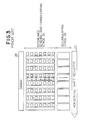
- the charge-coupled device largely comprises photo diodes 1 arranged in rows and columns, vertical shift registers 2 interlined with the adjacent two columns of the photo diodes, a horizontal shift register 3 coupled to the vertical shift registers 2, and a drain provided on the opposite side to the horizontal shift register 3.
- Each of the photo diodes 1 is represented by a small rectangle.
- a series of vertical driving pulses 4 takes place at a certain interval, and all of the electric charges are transferred to the outside thereof in a driving period between two vertical blanking time periods 6 as shown in Fig. 2.
- the charge-coupled device reported by Okumura intermittently produces two read-out pulses 7 and 8 in a single vertical blanking time period 6, and reverse transferring pulses 9 are further produced between the two read-out pulses 7 and 8.
- ineffectual electric charges are discharged from the photo diodes 1 to the vertical shift registers 2, and the ineffectual electric charges are reversely swept into the drain 4 through the vertical shift registers 2 in response to the reverse transferring pulses 9.
- the photo diodes 1 While sweeping the ineffectual electric charges into the drain 4, the photo diodes 1 accumulate fresh or effectual electric charges produced in the presence of an optical image.
- the electric charges thus accumulated in the photo diodes 1 are discharged to the vertical shift registers 2 in response to the second read-out pulse 8, and are successively transferred to the outside thereof in cooperation with the horizontal shift register 3.
- the vertical driving pulses 10 are produced in a driving time period between the two vertical blanking time periods 6 at a certain time interval.
- the photo diodes 1 are exposed to the optical image for an effective accumulation time period t1 between the two read-out pulses 7 and 8, and the shutter speed is then calculated from the effective accumulation time period t1.
- the effective accumulation time period t1 is about a thousandth second.
- the effective accumulation time period t1 is thus shrunk to the small value, the charge-coupled device can reproduce an optical image from a high-speed moving object.
- a charge-coupled device illustrated in Fig. 3 is proposed and aims at extension of the effective accumulation time period t1.
- the charge-coupled device shown in Fig. 3 largely comprises an interlined sensing-and-transferring stage 21, a horizontal shift register 22, an accumulating stage 23 provided between the interlined sensing-and-transferring stage 21 and the horizontal shift register 22, and a drain 24 provided on the opposite side of the accumulating stage 23.
- the charge-coupled device thus arranged completes the delivery of the ineffectual electric charges in the previous driving period, and only the reverse transferring pulses 9 and the second read-out pulse 8 take place in the vertical blanking time period 6. For this reason, the effective accumulation time period t1 is prolonged to a two hundreds and fiftieth second.
- the ineffective accumulation time period is four times to sixteen times longer than the effective accumulation time period t1, and, accordingly, the ineffectual electric charges are drastically increased to a saturation level which serves as a criterion of production of the blooming phenomenon.
- the saturation level is related to a blooming control voltage level.
- the ineffectual electric charges are transferred at about 800 KHz higher than the ordinary vertical transferring operation of the effective electric charges.
- the electrodes of the vertical shift registers 2 are relatively large in resistance and in capacitance due to double or tipple structure of polysilicon, and, for this reason, the driving pulses are delayed and deformed at the high frequency transferring operation. Thus, the driving pulses are delayed and deformed, so that the vertical shift registers deteriorate in the charge transferring capacity.
- the amount of the ineffectual electric charges transferred to the drain is decreased to a half or a third, leaving residual charges in the photo-sensitive elements. These residual charges are causative of electric signals over the saturation level, and the electric signals produces a white small jamming image.
- the length of the vertical blanking time period t1 sets a limitation on the number of the relaying operations for the sweeping operation. This results in insufficient sweeping operation.
- the wider screen the charge-coupled device is associated the more residual charges the charge-coupled device holds. If the blooming control voltage is regulated to a high level, there is a trade-off between the dynamic range and the amount of the residual charges.
- a charge coupled device according to the pre-characterizing part of the claim and a corresponding control method is disclosed in IEEE Transaction on Electron Devices, vol. ED-31, No. 1, January 1984, pages 83-88, by Y. Ishihara et al.
- a constant, probably selected voltage is supplied to the substrate in order to reduce blooming effects.
- EP-A-0 265 271 discloses a similar solid state imaging device, wherein the voltage supplied to the substrate can be switched between two values for reducing the amount of "ineffectual" electric charges in the photo-sensing elements.
- the present invention proposes to make the photo sensing elements less sensitive or less retainable in the ineffective accumulation time period.
- a controlling method for a charge-coupled device fabricated on a semiconductor substrate and comprising a plurality of photo sensing elements arranged in columns and operative to convert an optical radiation into electric charges, respectively, a multiple-stage horizontal shift register, an overflow drain, a plurality of multiple-stage vertical shift registers interlined with said columns of said photo sensing elements and operative to transfer said electric charges to one of said multiple-stage horizontal shift register and said overflow drain, and a photo shield film provided over said photo sensing elements in such a manner as to allow said optical radiation to impinge on the photo sensing elements, said controlling method being characterized by the steps of
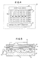
- a two-dimensional charge-coupled device is fabricated on an n-type single semiconductor substrate 30 and largely comprises a plurality of photo-sensing elements 31 each corresponding to a pixel and arranged in rows and columns, a plurality of multiple-stage vertical shift registers 32 each interlined with adjacent two columns of the photo-sensing elements 31, a multiple-stage horizontal shift register 33 coupled to first output nodes of the vertical shift registers 32, and an overflow drain 34 coupled to second output nodes of the vertical shift registers 32 and provided at the opposite ends to the horizontal shift register 33.
- the two-dimensional charge-coupled device thus arranged is classified into the interlined type with the vertical overflow drain structure.
- each of the photo-sensing elements 31 is formed by a photo diode, and the vertical shift register 32 is of the vertical CCD register type.
- the plural photo diodes and the plural vertical shift registers are fabricated on the semiconductor substrate 30, description is focused upon a single photo diode and a single vertical shift register.
- a p-type well 35 where a plurality of n-type regions 36, 37, 38 and 39 are formed and isolated by p-type impurity regions 40, 41 and 42.
- the p-type well 35 is reversely biased with respect to the n-type substrate 30, and the reverse biasing voltage level is variable by means of a controller 60.
- the major surface of the substrate 31 is covered with an oxide film 43 which is transparent to an optical radiation.
- the optical radiation carries an optical image from an object.
- the oxide film 43 is partially covered with conductive strips 44 serving as electrodes of the vertical shift register 32, and the entire surface is overlain by an oxide film 45 which is also transparent to the optical radiation.
- a photo-shield film 46 which is supplied with an appropriate positive biasing voltage level.
- the n-type region 37 and the p-type well 35 beneath the region 37 form in combination the photo diode, and the p-type impurity region 41 and the gate electrode 45 provide an input gate of the vertical shift register 32 bridging between the n-type region 37 and one of the n-type regions 38.
- the n-type regions 38 (only one of which is shown in the cross sectional view) are spaced apart from one another, and are respectively associated with the conductive strips or the gate electrodes 44 to form a plurality of transferring stages.
- the p-type impurity region 42 serves as a channel stopper between the vertical shift register 32 and the adjacent photo diode.
- the p-type impurity region 41, the n-type regions 38, and the gate electrodes 44 form the vertical shift register 32.
- Each of the vertical shift registers 32 has 250 gate electrodes 44 provided in parallel to one another, and, accordingly, is provided with 250 transferring stages.
- Each transferring stage performs a single transferring operation with a vertical driving pulse SHFT , and the amount of the maximum electric charge transferred is tantamount to the output voltage level of about 0.9 volt at15.75KHz.
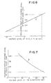
- the biasing voltage level directly affects the amount of the maximum electric charge produced by the photo diode forming each of the photo sensing elements 31, and is varied as the function indicated by plots A in Fig. 6. This is because of the fact that the lines of electric forces from the photo shield film 46 reach the surface of the photo diode and, accordingly, vary the voltage level of the surface.
- the amount of the maximum electric charge affected by the biasing voltage level is also capable of being represented by an output voltage level delivered from the horizontal shift register of the charge-coupled device to the outside thereof.
- the output voltage level thus representing the amount of the maximum electric charge produced by each photo diode is hereinbelow referred to as "saturated output voltage level".
- the saturated output voltage level of the photo diode is further varied as the function indicated by plots B of Fig. 7 with respect to the voltage level at the semiconductor substrate 30 when a certain voltage level is fixedly applied to the photo shield film 46.
- an electronic shutter of about a thousandth second is implemented by the charge-coupled device controlled by a method according to the present invention without any sacrifice of quality of an image reproduced on a screen.
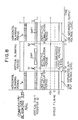
- Fig. 8 of the drawings horizontal blanking periods and vertical blanking periods appropriately take place, and electric charges respectively produced by the photo sensing elements 31 are delivered in succession from the horizontal shift register 33 of the charge-coupled device to the outside thereof in a single read-out cycle.
- Two read-out pulses 61 and 62 are produced in each vertical blanking period, and a series of high speed vertical driving pulses SWP takes place between the two read-out pulses 61 and 62 for sweeping ineffectual electric charges into the overflow drain 34.
- the first read-out pulse 61 takes place, the ineffectual electric charges accumulated in the photo sensing elements 31 are delivered to the vertical shift registers 32, and are transferred to the overflow drain 34 in the presence of the high speed vertical driving pulses SWP.
- each of the vertical shift registers 32 has the two hundreds and fifty transferring stages, however, five hundreds of the transferring operations are achieved at the high speed driving frequency of about 800 KHz.
- the high speed driving frequency the amount of transferring charge in a single transferring operation is turned into an output voltage level of about 0.3 volt which is a third achieved by an usual vertical transferring operation for the effectual electric charge, and the amount of the transferring charges is measured for the photo diode around the center of the pixel array.
- the ineffectual electric charges are accumulated in each of the horizontal blanking periods, and the photo shield film 44 is negatively biased to -5 volts.
- the saturated output voltage level is about 0.2 volt at the negative biassing voltage level of about -5 volts.
- the saturated output voltage level of about 0.2 volt is low enough to perfectly be swept with the high speed driving frequency of about 800 KHz, because the amount of the transferring charge is estimated as about 0.3 volt as described hereinbefore. This results in that no residual electric charge is left in the photo sensing elements.
- the first read-out pulse 61 is recovered at time t0, fresh effectual electric charges are accumulated in the photo sensing elements 31.
- the positive biasing voltage level of about +5 volts is applied to the photo shield film 44, and the saturated output voltage level is increased to about 0.8 volt with the biasing level of about +5 volts as will be seen from plots A of Fig. 6. Since the amount of the maximum transferring charge in the usual transferring operation is turned into about 0.9 volt, the saturated output voltage level of about 0.8 volt is slightly lower than the maximum transferring capacity of the vertical shift register, and, accordingly, a sufficiently wide dynamic range is established in the photo sensing elements. No residual electric charge is left in the photo sensing elements, and, for this reason, the blooming phenomenon is less liable to take place even if the wide dynamic range is established.
- the effectual electric charges are read-out from the photo sensing elements 31 to the vertical shift registers 32 in the presence of the second read-out pulse 62.
- the vertical shift registers 32 and the horizontal shift register 33 are responsive to the driving pulses SHFT and blanking pulses (not shown), and the effectual electric charges are relayed from the vertical shift registers 32 through the horizontal shift register 33 to the outside of the charge-coupled device.
- the photo shield film 46 is lowered to the negative biasing voltage level of about -5 volts again, so that a relatively small amount of ineffectual electric charge is merely produced in each of the photo sensing elements.
- the biasing voltage level is recovered to the negative value at time t2, and time t2 should be later than time t1 defining the trailing edge of the second read-out pulse 62.
- the recovery to the negative biasing voltage level is preferably adjusted in the vertical blanking period or the horizontal blanking period so as to prevent an optical image on the screen from some noises produced upon shifting.
- the ascent of the biasing voltage at time t3 is allowed to be later than the trailing edge of the first read-out pulse at time t0. However, it is desirable that time t3 is earlier than time t0, because the effective accumulation time period or the electronic shutter speed is proportional to the sensitivity.
- the charge-coupled device controlled by the method according to the present invention is free from the blooming phenomenon by virtue of shifting the voltage level at either of the photo shield film or the semiconductor substrate for reduction in the amount of the ineffectual electric charges.
- the transferring operations are as twice as large in number as the transferring stages, and the vertical shift registers can sweep the ineffectual electric charges as twice large as the maximum transferring charges.
- the biasing voltage level of the photo shield film 46 may be selected to be not greater than about 0.6 volt.
Landscapes
- Engineering & Computer Science (AREA)
- Multimedia (AREA)
- Signal Processing (AREA)
- Transforming Light Signals Into Electric Signals (AREA)
- Solid State Image Pick-Up Elements (AREA)
Claims (1)
- Regelungsverfahren für eine ladungsgekoppelte Anordnung, die auf einem Halbleitersubstrat (30) hergestellt ist, und aufweist: eine Anzahl lichtempfindlicher Elemente (31), die in Spalten angeordnet sind und betreibbar sind, um jeweils eine optische Strahlung in elektrische Ladungen umzuwandeln, ein mehrstufiges, horizontales Schieberegister (33), ein Überlaufdrain (34), eine Anzahl mehrstufiger, vertikaler Schieberegister (32), die zwischen den Spalten der lichtempfindlichen Elemente angeordnet sind und betreibbar sind, um die elektrischen Ladungen zu einem der mehrstufigen horizontalen Schieberegister und zu dem Überlaufdrain zu übertragen, und einen lichtabschirmenden Film (46), der über den lichtempfindlichen Elementen so vorgesehen ist, daß er der optischen Strahlung erlaubt, auf die lichtempfindlichen Elemente einzufallen, wobei das Regelungsverfahren durch die Schritte gekennzeichnet ist:a) Speicherung der wirksamen elektrischen Ladungen in Anwesenheit der optischen Strahlung in den lichtempfindlichen Elementen durch Anlegung eines ersten Spannungspegels an die lichtabschirmende Platte zur Förderung der Erzeugung der wirksamen elektrischen Ladungen, während unwirksame elektrische Ladungen in das Überflußdrain durch die mehrstufigen vertikalen Schieberegister synchron mit einem ersten Treiber-Pulszug (SWP) getrieben werden, nachdem die unwirksamen elektrischen Ladungen aus der Anzahl der lichtempfindlichen Elementen in die Anzahl von mehrstufigen vertikalen Schieberegistern in Anwesenheit eines ersten Ausleseimpulses (61) ausgelesen wurden,b) Auslesen der wirksamen elektrischen Ladungen in der Anwesenheit eines zweiten Ausleseimpulses (62), undc) Übertragen der wirksamen elektrischen Ladungen von der Anzahl mehrstufiger vertikaler Schieberegister synchron mit einem zweiten Treiber-Impulszug (SHFT) an die mehrstufigen horizontalen Schieberegister, unter Anlegung eines zweiten Spannungspegels an die lichtabschirmende Platte zur Einschränkung der Erzeugung der unwirksamen elektrischen Ladungen in den lichtempfindlichen Elementen.
Applications Claiming Priority (2)
| Application Number | Priority Date | Filing Date | Title |
|---|---|---|---|
| JP63148769A JPH022793A (ja) | 1988-06-15 | 1988-06-15 | 2次元ccd撮像素子の駆動方法 |
| JP148769/88 | 1988-06-15 |
Publications (3)
| Publication Number | Publication Date |
|---|---|
| EP0346905A2 EP0346905A2 (de) | 1989-12-20 |
| EP0346905A3 EP0346905A3 (de) | 1991-01-02 |
| EP0346905B1 true EP0346905B1 (de) | 1994-08-17 |
Family
ID=15460247
Family Applications (1)
| Application Number | Title | Priority Date | Filing Date |
|---|---|---|---|
| EP89110895A Expired - Lifetime EP0346905B1 (de) | 1988-06-15 | 1989-06-15 | Regelungsverfahren der elektronischen Überblendung für eine zweidimensionale ladungsgekoppelte Anordnung |
Country Status (4)
| Country | Link |
|---|---|
| US (1) | US4989095A (de) |
| EP (1) | EP0346905B1 (de) |
| JP (1) | JPH022793A (de) |
| DE (1) | DE68917533T2 (de) |
Families Citing this family (12)
| Publication number | Priority date | Publication date | Assignee | Title |
|---|---|---|---|---|
| JP2601933B2 (ja) * | 1990-04-13 | 1997-04-23 | 株式会社東芝 | 固体撮像装置 |
| US5463421A (en) * | 1992-05-30 | 1995-10-31 | Sony Corporation | Solid-state image apparatus which sweeps out independently ineffective electric charges so that the exposure period can be varied within a range from one field period to one frame period |
| JPH0638111A (ja) * | 1992-07-16 | 1994-02-10 | Nec Corp | 二次元電荷結合撮像素子の駆動方法 |
| JPH06164826A (ja) * | 1992-11-24 | 1994-06-10 | Toshiba Corp | 固体撮像装置とその駆動方法 |
| JP3847811B2 (ja) * | 1995-06-30 | 2006-11-22 | キヤノン株式会社 | 撮像装置 |
| US6803960B2 (en) * | 1999-12-22 | 2004-10-12 | Eastman Kodak Company | Optical test structure for measuring charge-transfer efficiency |
| JP2002185871A (ja) * | 2000-12-12 | 2002-06-28 | Sony Corp | 固体撮像素子及びその駆動方法 |
| US20020171752A1 (en) * | 2001-05-18 | 2002-11-21 | Baer Richard L. | Apparatus and method for reducing saturation artifacts in digital images captured using frame-transfer CCD sensor with reduced-height storage area |
| JP3885769B2 (ja) | 2003-06-02 | 2007-02-28 | ソニー株式会社 | 固体撮像装置および固体撮像装置の駆動方法 |
| CN101848336B (zh) * | 2010-03-26 | 2013-01-02 | 四川川大智胜软件股份有限公司 | 一种使ccd摄像机抗纵向光晕的方法 |
| JP7072362B2 (ja) * | 2017-09-26 | 2022-05-20 | ブリルニクス シンガポール プライベート リミテッド | 固体撮像装置、固体撮像装置の駆動方法、および電子機器 |
| CN113324328B (zh) * | 2021-05-11 | 2022-12-13 | Tcl空调器(中山)有限公司 | 制冷设备的屏蔽频率的确定方法、装置及存储介质 |
Family Cites Families (11)
| Publication number | Priority date | Publication date | Assignee | Title |
|---|---|---|---|---|
| JPS5339211B2 (de) * | 1973-10-26 | 1978-10-20 | ||
| JPS6033345B2 (ja) * | 1979-06-08 | 1985-08-02 | 日本電気株式会社 | 電荷転送撮像装置とその駆動方法 |
| JPS6038988A (ja) * | 1983-08-12 | 1985-02-28 | Victor Co Of Japan Ltd | 固体撮像素子を用いた静止画像撮像装置 |
| JPS61144176A (ja) * | 1984-12-18 | 1986-07-01 | Canon Inc | 撮像装置 |
| JP2526205B2 (ja) * | 1985-10-22 | 1996-08-21 | 松下電子工業株式会社 | 固体撮像装置の駆動方法 |
| DE3685198D1 (de) * | 1985-11-20 | 1992-06-11 | Nec Corp | Verfahren zum betrieb eines zweidimensionalen ladungsuebertragungsbildsensors. |
| US4875100A (en) * | 1986-10-23 | 1989-10-17 | Sony Corporation | Electronic shutter for a CCD image sensor |
| JPS63177664A (ja) * | 1987-01-19 | 1988-07-21 | Canon Inc | 電子スチルカメラ |
| US4856033A (en) * | 1987-03-06 | 1989-08-08 | Sony Corporation | Solid state imager device with exposure control with noise reduction |
| JP2523617B2 (ja) * | 1987-04-10 | 1996-08-14 | 松下電子工業株式会社 | 固体撮像装置の駆動方法 |
| US4834474A (en) * | 1987-05-01 | 1989-05-30 | The University Of Rochester | Optical systems using volume holographic elements to provide arbitrary space-time characteristics, including frequency-and/or spatially-dependent delay lines, chirped pulse compressors, pulse hirpers, pulse shapers, and laser resonators |
-
1988
- 1988-06-15 JP JP63148769A patent/JPH022793A/ja active Pending
-
1989
- 1989-06-13 US US07/365,310 patent/US4989095A/en not_active Expired - Fee Related
- 1989-06-15 EP EP89110895A patent/EP0346905B1/de not_active Expired - Lifetime
- 1989-06-15 DE DE68917533T patent/DE68917533T2/de not_active Expired - Fee Related
Also Published As
| Publication number | Publication date |
|---|---|
| EP0346905A3 (de) | 1991-01-02 |
| EP0346905A2 (de) | 1989-12-20 |
| JPH022793A (ja) | 1990-01-08 |
| US4989095A (en) | 1991-01-29 |
| DE68917533T2 (de) | 1995-03-30 |
| DE68917533D1 (de) | 1994-09-22 |
Similar Documents
| Publication | Publication Date | Title |
|---|---|---|
| US4322753A (en) | Smear and/or blooming in a solid state charge transfer image pickup device | |
| US4962412A (en) | Photoelectric conversion apparatus without isolation regions | |
| US3953733A (en) | Method of operating imagers | |
| EP0365000B1 (de) | CCD-Bildsensor mit vertikaler Überlauf-Senke | |
| US4450484A (en) | Solid states image sensor array having circuit for suppressing image blooming and smear | |
| US4302779A (en) | Methods of reducing blooming in the drive of charge-coupled image sensors | |
| US4349743A (en) | Solid-state imaging device | |
| US4774585A (en) | Image pickup apparatus | |
| EP0346905B1 (de) | Regelungsverfahren der elektronischen Überblendung für eine zweidimensionale ladungsgekoppelte Anordnung | |
| US4641183A (en) | Image pick-up apparatus | |
| US4551757A (en) | Method for driving solid-state image sensor | |
| JPS6369267A (ja) | 固体撮像装置の駆動方法 | |
| US4910588A (en) | Image pick-up apparatus with high resolution and anti-bloom characteristics | |
| US4589027A (en) | Solid state image sensor | |
| US4811068A (en) | Charge transfer device | |
| US5748232A (en) | Image sensor and driving method for the same | |
| US4794279A (en) | A solid state imaging device which applies two separate storage voltages for the signal charges so as to reduce the smear level and the dark current | |
| EP0022323B1 (de) | Festkörper-Bildzerlegungsvorrichtung | |
| US5757427A (en) | Image pick-up apparatus having a charge coupled device with multiple electrodes, a buffer layer located below some of the electrodes | |
| EP0372456B1 (de) | CCD-Bildwandler mit senkrechtem Ueberlaufdrain | |
| KR0127300B1 (ko) | 고체촬상장치 | |
| US4985776A (en) | Method of driving solid-state imaging element | |
| US4603343A (en) | Solid state image sensor applied with differing read-out gate voltages | |
| JPH0262170A (ja) | 固体撮像装置 | |
| JP2554621B2 (ja) | 固体撮像装置 |
Legal Events
| Date | Code | Title | Description |
|---|---|---|---|
| PUAI | Public reference made under article 153(3) epc to a published international application that has entered the european phase |
Free format text: ORIGINAL CODE: 0009012 |
|
| 17P | Request for examination filed |
Effective date: 19890615 |
|
| AK | Designated contracting states |
Kind code of ref document: A2 Designated state(s): DE FR GB |
|
| PUAL | Search report despatched |
Free format text: ORIGINAL CODE: 0009013 |
|
| AK | Designated contracting states |
Kind code of ref document: A3 Designated state(s): DE FR GB |
|
| 17Q | First examination report despatched |
Effective date: 19930223 |
|
| GRAA | (expected) grant |
Free format text: ORIGINAL CODE: 0009210 |
|
| AK | Designated contracting states |
Kind code of ref document: B1 Designated state(s): DE FR GB |
|
| PG25 | Lapsed in a contracting state [announced via postgrant information from national office to epo] |
Ref country code: FR Effective date: 19940817 |
|
| REF | Corresponds to: |
Ref document number: 68917533 Country of ref document: DE Date of ref document: 19940922 |
|
| EN | Fr: translation not filed | ||
| PLBE | No opposition filed within time limit |
Free format text: ORIGINAL CODE: 0009261 |
|
| STAA | Information on the status of an ep patent application or granted ep patent |
Free format text: STATUS: NO OPPOSITION FILED WITHIN TIME LIMIT |
|
| 26N | No opposition filed | ||
| PGFP | Annual fee paid to national office [announced via postgrant information from national office to epo] |
Ref country code: GB Payment date: 19990609 Year of fee payment: 11 |
|
| PGFP | Annual fee paid to national office [announced via postgrant information from national office to epo] |
Ref country code: DE Payment date: 19990618 Year of fee payment: 11 |
|
| PG25 | Lapsed in a contracting state [announced via postgrant information from national office to epo] |
Ref country code: GB Free format text: LAPSE BECAUSE OF NON-PAYMENT OF DUE FEES Effective date: 20000615 |
|
| GBPC | Gb: european patent ceased through non-payment of renewal fee |
Effective date: 20000615 |
|
| PG25 | Lapsed in a contracting state [announced via postgrant information from national office to epo] |
Ref country code: DE Free format text: LAPSE BECAUSE OF NON-PAYMENT OF DUE FEES Effective date: 20010403 |