EP0346028B1 - Videosignalanzeigegerät - Google Patents
Videosignalanzeigegerät Download PDFInfo
- Publication number
- EP0346028B1 EP0346028B1 EP89305616A EP89305616A EP0346028B1 EP 0346028 B1 EP0346028 B1 EP 0346028B1 EP 89305616 A EP89305616 A EP 89305616A EP 89305616 A EP89305616 A EP 89305616A EP 0346028 B1 EP0346028 B1 EP 0346028B1
- Authority
- EP
- European Patent Office
- Prior art keywords
- signal
- supplied
- video signal
- standard
- counter
- Prior art date
- Legal status (The legal status is an assumption and is not a legal conclusion. Google has not performed a legal analysis and makes no representation as to the accuracy of the status listed.)
- Expired - Lifetime
Links
Images


Classifications
-
- H—ELECTRICITY
- H04—ELECTRIC COMMUNICATION TECHNIQUE
- H04N—PICTORIAL COMMUNICATION, e.g. TELEVISION
- H04N9/00—Details of colour television systems
- H04N9/12—Picture reproducers
-
- H—ELECTRICITY
- H04—ELECTRIC COMMUNICATION TECHNIQUE
- H04N—PICTORIAL COMMUNICATION, e.g. TELEVISION
- H04N3/00—Scanning details of television systems; Combination thereof with generation of supply voltages
- H04N3/10—Scanning details of television systems; Combination thereof with generation of supply voltages by means not exclusively optical-mechanical
- H04N3/12—Scanning details of television systems; Combination thereof with generation of supply voltages by means not exclusively optical-mechanical by switched stationary formation of lamps, photocells or light relays
- H04N3/127—Scanning details of television systems; Combination thereof with generation of supply voltages by means not exclusively optical-mechanical by switched stationary formation of lamps, photocells or light relays using liquid crystals
-
- G—PHYSICS
- G09—EDUCATION; CRYPTOGRAPHY; DISPLAY; ADVERTISING; SEALS
- G09G—ARRANGEMENTS OR CIRCUITS FOR CONTROL OF INDICATING DEVICES USING STATIC MEANS TO PRESENT VARIABLE INFORMATION
- G09G3/00—Control arrangements or circuits, of interest only in connection with visual indicators other than cathode-ray tubes
- G09G3/20—Control arrangements or circuits, of interest only in connection with visual indicators other than cathode-ray tubes for presentation of an assembly of a number of characters, e.g. a page, by composing the assembly by combination of individual elements arranged in a matrix no fixed position being assigned to or needed to be assigned to the individual characters or partial characters
- G09G3/34—Control arrangements or circuits, of interest only in connection with visual indicators other than cathode-ray tubes for presentation of an assembly of a number of characters, e.g. a page, by composing the assembly by combination of individual elements arranged in a matrix no fixed position being assigned to or needed to be assigned to the individual characters or partial characters by control of light from an independent source
- G09G3/36—Control arrangements or circuits, of interest only in connection with visual indicators other than cathode-ray tubes for presentation of an assembly of a number of characters, e.g. a page, by composing the assembly by combination of individual elements arranged in a matrix no fixed position being assigned to or needed to be assigned to the individual characters or partial characters by control of light from an independent source using liquid crystals
- G09G3/3611—Control of matrices with row and column drivers
-
- G—PHYSICS
- G09—EDUCATION; CRYPTOGRAPHY; DISPLAY; ADVERTISING; SEALS
- G09G—ARRANGEMENTS OR CIRCUITS FOR CONTROL OF INDICATING DEVICES USING STATIC MEANS TO PRESENT VARIABLE INFORMATION
- G09G2340/00—Aspects of display data processing
- G09G2340/04—Changes in size, position or resolution of an image
- G09G2340/0407—Resolution change, inclusive of the use of different resolutions for different screen areas
- G09G2340/0414—Vertical resolution change
Definitions
- This invention relates to video signal display apparatus, and in particular to such display apparatus having a plurality of display elements such as liquid crystals or fluorescent phosphor tubes which are arranged in a two-dimensional manner or in an X-Y matrix shape.
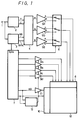
- Figure 1 of the accompanying drawings shows a previously-proposed display apparatus utilising, for example, a liquid crystal display panel.
- a video signal applied to a video input terminal 1 is supplied to a luminance signal and chroma signal (Y/C) separating circuit 2 which processes the video signal to provide a luminance signal Y and a chroma signal C.
- the video signal applied to the input terminal 1 is also supplied to a synchronising signal separating circuit 3, from which there are derived a horizontal synchronising signal HD and a synchronising signal SYNC.
- the luminance signal Y, the chrominance signal C, the horizontal synchronising signal HD and the synchronising signal SYNC are all supplied to an RGB decoder 4 which generates red, green and blue primary colour signals R, G and B.
- the red, green and blue primary colour signals R, G and B are respectively supplied to amplifiers 5R, 5G and 5B which generate signals of positive and negative polarities. These signals of positive and negative polarities are supplied to an alternate current drive switch 6.
- a composite synchronising signal from the separating circuit 3 is supplied to a display panel control signal generating circuit 7 which supplies a field pulse of alternate polarity at every field to the switch 6.
- the switch 6 generates red, green and blue signals R, G and B which are alternate current signals at every field.
- the red, green and blue signals R, G and B from the switch 6 are supplied to a data driver 8.
- the data driver 8 is also supplied with a picture element clock signal, a reset signal, a transfer timing signal and an output timing signal, all from the generating circuit 7, in synchronism with the horizontal synchronising signal. These signals are supplied through respective gate circuits 9a, 9b, 9c and 9d to the data driver 8.
- the generating circuit 7 supplies a reset signal synchronised with a vertical synchronising signal to a scan driver 10, and also supplies a horizontal synchronising signal HD through a gate circuit 11 to the scan driver 10.
- the data driver 8 and the scan driver 10 drive a display panel 12, whereby the video signal applied to the terminal 1 is sampled at every pixel by the data driver 8 and is supplied to the display panel 12 in response to the transfer timing signal and to the output timing signal, while the scan driver 10 sequentially selects the respective horizontal scanning lines, thereby displaying a video image on the display panel 12.
- the display panel 12 might have 512 display scanning lines which correspond to an effective picture area according to, for example, the NTSC system.
- the effective picture area according to the CCIR system has more than 600 display scanning lines, and in the manufacturing process of this kind of display panel, the manufacturing yield is not satisfactory.
- the demand for display panels according to the CCIR system is expected to be very small compared with that for display panels according to the NTSC system.
- a video image according to the CCIR system be displayed on a display panel of the NTSC system.
- the ratio between the CCIR and NTSC horizontal scanning lines is about 6 : 5, whereby the video image according to the CCIR system can be displayed on the display panel according to the NTSC system by discarding the horizontal scanning lines of the video image according to the CCIR system in the ratio of 6 : 1, in other words discarding every sixth line.
- the generating circuit 7 supplies the horizontal synchronising signal HD and the reset signal synchronised with the vertical synchronising signal to a counter 13, and the output signal from the counter 13 is used to control the gate circuits 9a to 9d and the gate circuit 11.
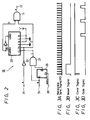
- the counter 13 effects the required removal of the horizontal scanning lines, and will be described more fully with reference to a block diagram shown in Figure 2 of the accompanying drawings, waveforms of signals in Figure 2 being shown in Figures 3A to 3D of the accompanying drawings.
- like parts corresponding to those of Figure 1 are marked with the same references and therefore will not be described in detail.
- the horizontal synchronising signal HD from the generating circuit 7 ( Figure 1) is supplied to a terminal 21.
- the signal from the terminal 21 is supplied through an inverter 22 to a clock input terminal CK of a 16-scale counter 23.
- the waveform of the signal applied to the terminal 21 is shown in Figure 3A.
- the reset signal synchronised with the vertical synchronising signal is supplied to a terminal 24 from the generating circuit 7 (shown in Figure 1), and the reset signal from the terminal 24 is fed to a D input terminal of a D flip-flop 25.
- the waveform of the reset signal is illustrated in Figure 3B.
- a clock signal having a frequency of, for example, 4 MHz applied to a terminal 26 is supplied to a clock input terminal CK of the D flip-flop 25.
- the output signal developed at the Q output terminal of the D flip-flop 25 and the reset signal from the terminal 24 are supplied to a NAND circuit 27.
- the output (whose waveform is illustrated in Figure 3C) from the NAND circuit 27 is fed to the clear input terminal CL of the counter 23.
- a signal "0" (1 ow level) is supplied to the data input terminal A (least significant bit) and to the data input terminal C, whereas a signal "1" (high level) is supplied to the data input terminal B and to the data input terminal D (most significant bit).
- Data representing [10] (decimal value) is therefore supplied to the counter 23.
- the carry output of the counter 23 is supplied through an inverter 28 to the load input terminal LOAD of the counter 23.
- the NAND circuit 27 when the horizontal synchronising signal HD shown in Figure 3A is supplied to the terminal 21 and the reset signal shown in Figure 38 is supplied to the terminal 24, the NAND circuit 27 derives the clear signal whose waveform is shown in Figure 3C.
- the signal from the NAND circuit 27 is supplied to the clear terminal CL of the counter 23, whereby the counter 23 derives a carry output when counting the horizontal synchronising signal HD from the terminal 21 sixteen times after having received the signal at its clear input terminal CL. Further, when this carry output is supplied to the load input terminal LOAD of the counter 23, the data representing [10] is loaded into the counter 23. Thereafter, the counter 23 generates the carry output each time it counts the signal from the terminal 21 six times as shown in Figure 3D.
- the NOR circuit 11 When the carry output and the signal from the terminal 21 are supplied to the gate circuit (NOR circuit) 11, the NOR circuit 11 generates at its output terminal 11′ the horizontal synchronising signal HD whose pulse is removed every other six pulses as shown by a phantom outline in Figure 3A.
- the thus-processed horizontal synchronising signal HD is supplied to the scan driver 10 ( Figure 1), whereby during the period of the removed horizontal synchronising signal, the horizontal scanning position of the display panel 12 is not advanced and the signals from the data driver 8 are ignored, thus resulting in the pulse of the horizontal synchronising signal being removed. In that event, the supply of the clock signal, the reset signal, the transfer timing signal and the output timing signal from the generating circuit 7 to the data driver 8 is stopped by the gate circuits 9a to 9d, whereby a disturbance can be prevented from being caused by an undesired signal.
- the video image according to the CCIR system can be displayed on the NTSC display panel by removing the scanning lines in the ratio of 6 : 1.
- the position of the horizontal scanning line at which the pulse is removed is fixed as the position of every sixth horizontal scanning line on the basis of, for example, the sixteenth horizontal scanning line from the vertical synchronising signal (the reset signal).
- the vertical synchronising signal the reset signal.
- US Patent No. US-A-4 500 930 discloses a television standards converter which uses a video tape recorder (VTR).
- VTR video tape recorder
- the capstan speed of the VTR is that of the video signal recorded on the tape (namely at the original standard) whereas the drum speed is that of the new standard to which the video signal is being converted.
- the video signal reproduced by the VTR has the original line rate but the new (converted) field rate.
- a line rate converter converts the reproduced signal to the new line rate, thereby completing standards conversion of the video signal ready for display according to the new standard.
- apparatus for displaying a video signal corresponding to a first television standard, said apparatus having a plurality of display elements disposed in an X-Y matrix shape, said apparatus comprising: separator means for separating a sync signal from an input video signal; generator means for generating a control signal in response to said sync signal; drive means for driving said display elements in response to said video signal and said control signal; and converter means for changing the number of scanning lines in the input video signal when said input video signal is of a second standard different from said first standard, said converter means deleting or adding lines from or to said input video signal at times which differ from picture to picture.
- a preferred embodiment of the present invention described hereinafter provides an improved display apparatus that can overcome the above-mentioned defects inherent in the previously-proposed apparatus of Figures 1 and 2.
- the preferred display apparatus can prevent the scanning line-converted position from becoming conspicuous, and can therefore display video images satisfactorily.
- Figure 5 illustrates a main portion of display apparatus embodying the present invention.
- like parts corresponding to those of Figures 1 and 2 are marked with the same references.
- the horizontal synchronising signal HD from the generating circuit 7 is supplied to a terminal 31.
- the horizontal synchronising signal HD applied to the terminal 31 is supplied through an inverter 32 to a clock input terminal CK of a 16-scale counter 33.
- data representing "0" (low level) is supplied to the data input terminals A and C
- data representing "1" (high level) is supplied to the data input terminals B and D so that the value [10] is supplied to the counter 33 as the input data.
- data representing "1" is fed to the clear input terminal CL of the counter 33.
- the carry output of the counter 33 is supplied through an inverter 34 to the load input terminal LOAD of the counter 33.
- the counter 33 generates a carry output each time it counts six times the horizontal synchronising signal HD from the terminal 31 in the stationary state.
- the NOR circuit 11 When the carry output and the horizontal synchronising signal HD from the terminal 31 are supplied to the gate circuit (NOR circuit 11), the NOR circuit 11 generates at its output terminal 11′ a horizontal synchronising signal HD in which five sampling pulses are selected and one sampling pulse is rejected.
- the resultant horizontal synchronising signal HD is supplied to the scan driver 10 (see Figure 1) whereby during the period of the horizontal synchronising signal HD, the horizontal scanning position on the display panel 12 ( Figure 1) is not advanced and the signal fed from the data driver 8 ( Figure 1) during this period is inhibited; thus the scanning lines are selectively removed. Simultaneously, the supply of the clock signal, the reset signal, the transfer timing signal and the output timing signal from the generating circuit 7 to the data driver 8 is stopped by the gate circuits 9a to 9d in Figure 1.
- the CCIR system for example, employs 625 horizontal scanning lines per frame, and one line is left as a remainder when 625 is divided by six, whereby the position in which the horizontal scanning line is converted is sequentially changed with every frame.
- the position at which the horizontal scanning line is converted is varied with every frame so that the conversion position is not conspicuous. Hence, the video image can be displayed faithfully.
- Figure 6 illustrates a main portion of another embodiment of display apparatus.
- like parts corresponding to those of Figure 5 are marked with the same references and will not be further described.
- the signal applied to the input terminal 31 is supplied through the inverter 32 to the clock terminal CK of the counter 33.
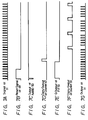
- the waveform of this signal applied to the input terminal 31 is shown in Figure 7A.
- a clock signal having a frequency of, for example, 4 MHz from a terminal 35 is supplied to a clock terminal CK of a counter 46.
- the count outputs QA, QB, QC and QD of the counter 46 are supplied to data input terminals A to D of a further counter 47.
- the signal from the inverter 32 is supplied to the clock input terminal CK of the counter 47.
- the reset signal synchronised with the vertical synchronising signal from the generating circuit 7 is supplied to a terminal 48.
- the signal from the terminal 48 is supplied to a D input terminal of a D flip-flop 49.
- the waveform of the reset signal is shown in Figure 7B.
- the D flip-flop 49 is also supplied at its clock input terminal CK with the signal at 4 MHz from the terminal 35.
- the Q output of the D flip-flop 49 and the reset signal applied to the terminal 48 are supplied to a NAND circuit 50.
- the output of the NAND circuit 50 is supplied to the load input terminal LOAD of the counter 47 and is also fed to the set input terminal of the flip-flop 51.
- the waveform of the output of the NAND circuit 50 is shown in Figure 7C.
- the carry output from the counter 47 is supplied through an inverter 52 to the reset input terminal of the flip-flop 51.
- the waveform of the carry output from the counter 47 is represented in Figure 7D.
- the Q output of the flip-flop 51 and the carry output of the counter 33 are mixed by a NOR circuit 54′, and the mixed output from the NOR circuit 54′ is fed to the load input terminal LOAD of the counter 33.
- the NAND circuit 50 derives the signal whose waveform is shown in Figure 7C.
- the signal from the NAND circuit 50 is supplied to the load input terminal LOAD of the counter 47, the count value of the counter 46 at that time is loaded into the counter 47.
- the count value to be loaded into the counter 47 is randomly determined by the counter 46.
- the counter 47 derives a carry output whose waveform is illustrated in Figure 7D. This carry output is supplied through the inverter 52 to the reset terminal of the flip-flop 51 so that the flip-flop 51 is reset to generate the Q output whose waveform is shown in Figure 7E.
- the trailing edge of the Q output from the flip-flop 51 is determined by the value to be loaded into the counter 47, and this load value is randomly determined by the counter 46.
- the Q output of the flip-flop 51 is supplied through the NOR circuit 54′ to the load input terminal LOAD of the counter 33, whereby data representing [10] is loaded into the counter 33.
- the carry output of the counter 33 is supplied to its load input terminal LOAD so that the counter 33 generates a carry output shown in Figure 7F each time it counts the signal from the terminal 31 six times.
- the NOR circuit 11 when the carry output and the signal from the terminal 31 are supplied to the gate circuit (NOR circuit) 11, the NOR circuit 11 generates at its output terminal 11′ a horizontal synchronising signal HD in which five pulses are selected and one pulse is removed as shown in Figure 7G.
- the timing of the first loading operation executed at every vertical synchronising signal in the counter 33 is randomly determined by the count value of the counter 46, whereby the timing is randomly varied in each frame.
- the scanning line conversion position can be prevented from becoming conspicuous and a faithful display can always be effected.
Landscapes
- Engineering & Computer Science (AREA)
- Chemical & Material Sciences (AREA)
- Crystallography & Structural Chemistry (AREA)
- Signal Processing (AREA)
- Multimedia (AREA)
- Theoretical Computer Science (AREA)
- General Physics & Mathematics (AREA)
- Computer Hardware Design (AREA)
- Physics & Mathematics (AREA)
- Transforming Electric Information Into Light Information (AREA)
- Control Of Indicators Other Than Cathode Ray Tubes (AREA)
- Video Image Reproduction Devices For Color Tv Systems (AREA)
- Liquid Crystal Display Device Control (AREA)
- Television Systems (AREA)
Claims (7)
- Gerät zur Anzeige eines einer ersten Fernsehnorm entsprechenden Videosignals mit einer Mehrzahl von in einer X-Y-Matrix angeordneten Anzeigeelementen,
wobei das Gerät aufweist:
eine Trenneinrichtung (3) zum Abtrennen eines Synchronisiersignals aus einem Eingangs-Videosignal,
eine Generatoreinrichtung (7) zur Erzeugung eines Steuersignals in Abhängigkeit von dem Synchronisiersignal,
eine Treibereinrichtung (8) zur Ansteuerung der Anzeigeelemente in Abhängigkeit von dem Videosignal und dem Steuersignal und
eine Wandlereinrichtung (13) zur Änderung der Zahl der Abtastzeilen in dem Eingangs-Videosignal, wenn dieses einer von der ersten Fernsehnorm abweichenden zweiten Fernsehnorm entspricht, wobei diese Wandlereinrichtung (13) in von Bild zu Bild differierenden Zeiten aus dem Eingangs-Videosignal Zeilen ausläßt oder dem Eingangs-Videosignal Zeilen hinzufügt. - Gerät nach Anspruch 1, bei dem die Wandlereinrichtung (13) die Zeitlage von ausgelassenen oder zugefügten Zeilen in Abhängigkeit von jedem Bildwechsel verschiebt.
- Gerät nach Anspruch 1, bei dem die Wandlereinrichtung (13) die Zeitlage von ausgelassenen oder zugefügten Zeilen in jedem Bild willkürlich ändert.
- Gerät nach Anspruch 1, 2 oder 3, bei dem die genannten Abtastzeilen bei der zweiten Fernsehnorm bei jeweils einer aus einer vorbestimmten Anzahl von Zeilen ausgelassen werden, wenn die Zahl der Abtastzeilen bei der zweiten Fernsehnorm größer ist als bei der ersten Fernsehnorm.
- Gerät nach Anspruch 4, bei dem die vorbestimmte Anzahl gleich sechs ist.
- Gerät nach einem der vorhergehenden Ansprüche, bei dem die erste Fernsehnorm die NTSC-Norm und die zweite Fernsehnorm eine CCIR-Norm ist.
- Gerät nach einem der vorhergehenden Ansprüche, bei dem die Anzeigeelemente Flüssigkristall-Panele sind.
Priority Applications (1)
| Application Number | Priority Date | Filing Date | Title |
|---|---|---|---|
| AT89305616T ATE99854T1 (de) | 1988-06-06 | 1989-06-02 | Videosignalanzeigegeraet. |
Applications Claiming Priority (2)
| Application Number | Priority Date | Filing Date | Title |
|---|---|---|---|
| JP139133/88 | 1988-06-06 | ||
| JP63139133A JP2913641B2 (ja) | 1988-06-06 | 1988-06-06 | X−yマトリクス型表示装置 |
Publications (3)
| Publication Number | Publication Date |
|---|---|
| EP0346028A2 EP0346028A2 (de) | 1989-12-13 |
| EP0346028A3 EP0346028A3 (en) | 1990-07-04 |
| EP0346028B1 true EP0346028B1 (de) | 1994-01-05 |
Family
ID=15238301
Family Applications (1)
| Application Number | Title | Priority Date | Filing Date |
|---|---|---|---|
| EP89305616A Expired - Lifetime EP0346028B1 (de) | 1988-06-06 | 1989-06-02 | Videosignalanzeigegerät |
Country Status (6)
| Country | Link |
|---|---|
| US (1) | US5003388A (de) |
| EP (1) | EP0346028B1 (de) |
| JP (1) | JP2913641B2 (de) |
| KR (1) | KR100189302B1 (de) |
| AT (1) | ATE99854T1 (de) |
| DE (1) | DE68911993T2 (de) |
Families Citing this family (8)
| Publication number | Priority date | Publication date | Assignee | Title |
|---|---|---|---|---|
| US5301031A (en) * | 1990-01-23 | 1994-04-05 | Hitachi Ltd. | Scanning conversion display apparatus |
| JPH0591447A (ja) * | 1991-09-25 | 1993-04-09 | Toshiba Corp | 透過形液晶表示装置 |
| GB9207527D0 (en) * | 1992-04-07 | 1992-05-20 | Philips Electronics Uk Ltd | Multi-standard video matrix display apparatus and its method of operation |
| US5381182A (en) * | 1993-09-28 | 1995-01-10 | Honeywell Inc. | Flat panel image reconstruction interface for producing a non-interlaced video signal |
| JP2869006B2 (ja) * | 1994-10-13 | 1999-03-10 | インターナショナル・ビジネス・マシーンズ・コーポレイション | 映像信号処理装置及び映像信号処理方法 |
| JPH08237561A (ja) * | 1995-02-24 | 1996-09-13 | Canon Inc | 表示装置及び記録再生装置 |
| EP1646027A1 (de) * | 2004-10-06 | 2006-04-12 | Harman Becker Automotive Systems GmbH | Videodaten Skalierungsschaltung |
| CN109637425A (zh) * | 2019-01-29 | 2019-04-16 | 惠科股份有限公司 | 一种驱动方法、驱动模块和显示装置 |
Family Cites Families (8)
| Publication number | Priority date | Publication date | Assignee | Title |
|---|---|---|---|---|
| US4500930A (en) * | 1982-05-26 | 1985-02-19 | Rca Corporation | Television signal standards conversion using a helical scan VTR |
| AU560269B2 (en) * | 1982-09-22 | 1987-04-02 | Philips Electronics N.V. | Field number conversion |
| FR2535562A1 (fr) * | 1982-10-27 | 1984-05-04 | Radiotechnique | Procede et circuit pour engendrer un signal de synchronisation de trame dans un recepteur d'images |
| US4642628A (en) * | 1984-06-22 | 1987-02-10 | Citizen Watch Co., Ltd. | Color liquid crystal display apparatus with improved display color mixing |
| US4694337A (en) * | 1986-01-23 | 1987-09-15 | Princeton Electronics Products, Inc. | Video line rate converter |
| JPS62159068U (de) * | 1986-03-31 | 1987-10-08 | ||
| JPS62269197A (ja) * | 1986-05-16 | 1987-11-21 | セイコーインスツルメンツ株式会社 | 液晶表示装置 |
| US4897799A (en) * | 1987-09-15 | 1990-01-30 | Bell Communications Research, Inc. | Format independent visual communications |
-
1988
- 1988-06-06 JP JP63139133A patent/JP2913641B2/ja not_active Expired - Lifetime
-
1989
- 1989-05-30 US US07/358,241 patent/US5003388A/en not_active Expired - Lifetime
- 1989-06-02 KR KR1019890007569A patent/KR100189302B1/ko not_active Expired - Lifetime
- 1989-06-02 AT AT89305616T patent/ATE99854T1/de not_active IP Right Cessation
- 1989-06-02 EP EP89305616A patent/EP0346028B1/de not_active Expired - Lifetime
- 1989-06-02 DE DE68911993T patent/DE68911993T2/de not_active Expired - Lifetime
Non-Patent Citations (1)
| Title |
|---|
| PATENT ABSTRACTS OF JAPAN vol. 12, no. 101 (E-595)(2948), 2 April 1988; & JP-A-62 232279 (CITIZEN WATCH) 12-10-1987 * |
Also Published As
| Publication number | Publication date |
|---|---|
| US5003388A (en) | 1991-03-26 |
| DE68911993T2 (de) | 1994-07-07 |
| KR900000827A (ko) | 1990-01-31 |
| EP0346028A3 (en) | 1990-07-04 |
| DE68911993D1 (de) | 1994-02-17 |
| EP0346028A2 (de) | 1989-12-13 |
| ATE99854T1 (de) | 1994-01-15 |
| JPH01307388A (ja) | 1989-12-12 |
| JP2913641B2 (ja) | 1999-06-28 |
| KR100189302B1 (ko) | 1999-06-01 |
Similar Documents
| Publication | Publication Date | Title |
|---|---|---|
| US4364090A (en) | Method for a compatible increase in resolution in television systems | |
| EP0326327B1 (de) | Vorrichtung zur Überlagerung von graphischen Bildtitelsignalen auf einem Videosignal | |
| US5488431A (en) | Video data formatter for a multi-channel digital television system without overlap | |
| US4720745A (en) | Method and apparatus for enhancing video displays | |
| US5534940A (en) | Apparatus and method for driving a liquid crystal display utilizing various television system formats | |
| US6384867B1 (en) | Video display apparatus capable of displaying video signals of a plurality of types with different specifications | |
| US5489945A (en) | Timing logic system and method for selectably controlling a high resolution charge coupled device image sensor of the type having two line pixel registers to provide a high resolution mode and alternatively a television resolution mode of picture imaging | |
| EP0096627A2 (de) | Interaktives Informationsanzeigesystem mit einem Rechner | |
| JPH05241524A (ja) | ユニバーサルビデオ出力装置 | |
| JPH0652938B2 (ja) | 液晶表示装置 | |
| EP0346028B1 (de) | Videosignalanzeigegerät | |
| JPS60263139A (ja) | 画像記録装置 | |
| JPH0834560B2 (ja) | モザイク効果発生装置 | |
| EP0507253B1 (de) | Vorrichtung zur Umwandlung eines Videoeingangssignals in ein kinematographisches Filmbild | |
| CA2105131C (en) | Image processing apparatus | |
| US7202900B2 (en) | Method of producing frame pair signals from an image sensor and method for displaying same | |
| EP0501462B1 (de) | Anzeigegerät | |
| US5440342A (en) | Logic system and method for controlling any one of different charge coupled device image sensors to provide video image signals in accordance with a television standard | |
| CN1116806A (zh) | 在数字视频重放系统中处理静止画面的装置 | |
| JPH055114B2 (de) | ||
| JP2708038B2 (ja) | 液晶ディスプレイ装置 | |
| SU1021024A1 (ru) | Устройство отображени информации на большом экране | |
| JP2670200B2 (ja) | 画像データ再生装置における間引回路 | |
| JP2823234B2 (ja) | 画面表示装置 | |
| JP3440491B2 (ja) | スーパーインポーズ装置 |
Legal Events
| Date | Code | Title | Description |
|---|---|---|---|
| PUAI | Public reference made under article 153(3) epc to a published international application that has entered the european phase |
Free format text: ORIGINAL CODE: 0009012 |
|
| AK | Designated contracting states |
Kind code of ref document: A2 Designated state(s): AT DE GB IT NL |
|
| PUAL | Search report despatched |
Free format text: ORIGINAL CODE: 0009013 |
|
| AK | Designated contracting states |
Kind code of ref document: A3 Designated state(s): AT DE GB IT NL |
|
| 17P | Request for examination filed |
Effective date: 19901128 |
|
| 17Q | First examination report despatched |
Effective date: 19920928 |
|
| GRAA | (expected) grant |
Free format text: ORIGINAL CODE: 0009210 |
|
| AK | Designated contracting states |
Kind code of ref document: B1 Designated state(s): AT DE GB IT NL |
|
| REF | Corresponds to: |
Ref document number: 99854 Country of ref document: AT Date of ref document: 19940115 Kind code of ref document: T |
|
| REF | Corresponds to: |
Ref document number: 68911993 Country of ref document: DE Date of ref document: 19940217 |
|
| ITF | It: translation for a ep patent filed | ||
| ITTA | It: last paid annual fee | ||
| PLBE | No opposition filed within time limit |
Free format text: ORIGINAL CODE: 0009261 |
|
| STAA | Information on the status of an ep patent application or granted ep patent |
Free format text: STATUS: NO OPPOSITION FILED WITHIN TIME LIMIT |
|
| 26N | No opposition filed | ||
| REG | Reference to a national code |
Ref country code: GB Ref legal event code: IF02 |
|
| PGFP | Annual fee paid to national office [announced via postgrant information from national office to epo] |
Ref country code: AT Payment date: 20080612 Year of fee payment: 20 |
|
| PGFP | Annual fee paid to national office [announced via postgrant information from national office to epo] |
Ref country code: IT Payment date: 20080625 Year of fee payment: 20 |
|
| PGFP | Annual fee paid to national office [announced via postgrant information from national office to epo] |
Ref country code: DE Payment date: 20080605 Year of fee payment: 20 Ref country code: NL Payment date: 20080603 Year of fee payment: 20 |
|
| PGFP | Annual fee paid to national office [announced via postgrant information from national office to epo] |
Ref country code: GB Payment date: 20080604 Year of fee payment: 20 |
|
| REG | Reference to a national code |
Ref country code: GB Ref legal event code: PE20 Expiry date: 20090601 |
|
| PG25 | Lapsed in a contracting state [announced via postgrant information from national office to epo] |
Ref country code: NL Free format text: LAPSE BECAUSE OF EXPIRATION OF PROTECTION Effective date: 20090602 |
|
| NLV7 | Nl: ceased due to reaching the maximum lifetime of a patent |
Effective date: 20090602 |
|
| PG25 | Lapsed in a contracting state [announced via postgrant information from national office to epo] |
Ref country code: GB Free format text: LAPSE BECAUSE OF EXPIRATION OF PROTECTION Effective date: 20090601 |