EP0345487A1 - Sputterverfahren zur Erzeugung einer Dünnschicht - Google Patents
Sputterverfahren zur Erzeugung einer Dünnschicht Download PDFInfo
- Publication number
- EP0345487A1 EP0345487A1 EP89108689A EP89108689A EP0345487A1 EP 0345487 A1 EP0345487 A1 EP 0345487A1 EP 89108689 A EP89108689 A EP 89108689A EP 89108689 A EP89108689 A EP 89108689A EP 0345487 A1 EP0345487 A1 EP 0345487A1
- Authority
- EP
- European Patent Office
- Prior art keywords
- pressure
- flow rate
- sputtering
- gas
- sputtering chamber
- Prior art date
- Legal status (The legal status is an assumption and is not a legal conclusion. Google has not performed a legal analysis and makes no representation as to the accuracy of the status listed.)
- Granted
Links
Images


Classifications
-
- C—CHEMISTRY; METALLURGY
- C23—COATING METALLIC MATERIAL; COATING MATERIAL WITH METALLIC MATERIAL; CHEMICAL SURFACE TREATMENT; DIFFUSION TREATMENT OF METALLIC MATERIAL; COATING BY VACUUM EVAPORATION, BY SPUTTERING, BY ION IMPLANTATION OR BY CHEMICAL VAPOUR DEPOSITION, IN GENERAL; INHIBITING CORROSION OF METALLIC MATERIAL OR INCRUSTATION IN GENERAL
- C23C—COATING METALLIC MATERIAL; COATING MATERIAL WITH METALLIC MATERIAL; SURFACE TREATMENT OF METALLIC MATERIAL BY DIFFUSION INTO THE SURFACE, BY CHEMICAL CONVERSION OR SUBSTITUTION; COATING BY VACUUM EVAPORATION, BY SPUTTERING, BY ION IMPLANTATION OR BY CHEMICAL VAPOUR DEPOSITION, IN GENERAL
- C23C14/00—Coating by vacuum evaporation, by sputtering or by ion implantation of the coating forming material
- C23C14/22—Coating by vacuum evaporation, by sputtering or by ion implantation of the coating forming material characterised by the process of coating
- C23C14/54—Controlling or regulating the coating process
- C23C14/548—Controlling the composition
-
- C—CHEMISTRY; METALLURGY
- C23—COATING METALLIC MATERIAL; COATING MATERIAL WITH METALLIC MATERIAL; CHEMICAL SURFACE TREATMENT; DIFFUSION TREATMENT OF METALLIC MATERIAL; COATING BY VACUUM EVAPORATION, BY SPUTTERING, BY ION IMPLANTATION OR BY CHEMICAL VAPOUR DEPOSITION, IN GENERAL; INHIBITING CORROSION OF METALLIC MATERIAL OR INCRUSTATION IN GENERAL
- C23C—COATING METALLIC MATERIAL; COATING MATERIAL WITH METALLIC MATERIAL; SURFACE TREATMENT OF METALLIC MATERIAL BY DIFFUSION INTO THE SURFACE, BY CHEMICAL CONVERSION OR SUBSTITUTION; COATING BY VACUUM EVAPORATION, BY SPUTTERING, BY ION IMPLANTATION OR BY CHEMICAL VAPOUR DEPOSITION, IN GENERAL
- C23C14/00—Coating by vacuum evaporation, by sputtering or by ion implantation of the coating forming material
- C23C14/22—Coating by vacuum evaporation, by sputtering or by ion implantation of the coating forming material characterised by the process of coating
- C23C14/56—Apparatus specially adapted for continuous coating; Arrangements for maintaining the vacuum, e.g. vacuum locks
- C23C14/564—Means for minimising impurities in the coating chamber such as dust, moisture, residual gases
-
- C—CHEMISTRY; METALLURGY
- C23—COATING METALLIC MATERIAL; COATING MATERIAL WITH METALLIC MATERIAL; CHEMICAL SURFACE TREATMENT; DIFFUSION TREATMENT OF METALLIC MATERIAL; COATING BY VACUUM EVAPORATION, BY SPUTTERING, BY ION IMPLANTATION OR BY CHEMICAL VAPOUR DEPOSITION, IN GENERAL; INHIBITING CORROSION OF METALLIC MATERIAL OR INCRUSTATION IN GENERAL
- C23C—COATING METALLIC MATERIAL; COATING MATERIAL WITH METALLIC MATERIAL; SURFACE TREATMENT OF METALLIC MATERIAL BY DIFFUSION INTO THE SURFACE, BY CHEMICAL CONVERSION OR SUBSTITUTION; COATING BY VACUUM EVAPORATION, BY SPUTTERING, BY ION IMPLANTATION OR BY CHEMICAL VAPOUR DEPOSITION, IN GENERAL
- C23C14/00—Coating by vacuum evaporation, by sputtering or by ion implantation of the coating forming material
- C23C14/22—Coating by vacuum evaporation, by sputtering or by ion implantation of the coating forming material characterised by the process of coating
- C23C14/34—Sputtering
Definitions
- the present invention relates to a method for fabricating thin films of various materials by electric glow discharge in gas. Especially it relates to a sputtering method having a high sputtering efficiency at low gas pressure which assures a low contamination and high grade of the sputtered film, still keeping low consumption of the gas.
- Sputtered thin films are used in variety of industries, such as production of semiconductor devices, thin film circuit board, optical equipments and so on. There are several methods for forming thin films. Among them the electrical sputtering is one of the most widely used method, and it can be applied for sputtering various materials such as metal, dielectric or semiconductor materials.
- Sputtering is a method to bombard a material to be sputtered with ions in a plasma formed by electric discharge, and sputter the material to form a film on an object. Recently, in order to increase the sputtering efficiency, a magnetic field is applied to focus the ion stream on the target formed by the material to be sputtered. Such method is called in the art magnetron sputtering.
- the maintenance of the sputtering equipment must be very careful.
- the sputtering chamber should be degased by baking it in vacuum before it is used, and the inert gas is purified. Still some impurities stray into the plasma, and cause contamination of the sputtered film. This decreases the reliability of the device and the production yield. Such contamination is considered to be due to a minute leakage of the sputtering chamber and residual gas which are very difficult to perfectly remove by preliminary degassing.
- the residual gas is brought into the sputtering chamber together with the object itself. For example, if an aluminum film is formed over a phosphosilicate glass (PSG) substrate, the humidity is easily adsorbed by PSG and brought into the sputtering chamber. The adsorbed humidity is released by the sputtering, and poisons the sputtered aluminum film.
- PSG phosphosilicate glass
- an ion plasma is formed by glow discharge in argon gas at a pressure of about 10 ⁇ 3 Torr.
- argon gas there is a range of desirable pressure for keeping a stable plasma in the sputtering chamber. Too higher or lower pressure than the desirable pressure can not maintain a stable electric discharge, and can not keep a stable plasma.
- the pressure of gas in the sputtering chamber is controlled by injecting inert gas, argon for example, into the chamber or controlling the pumping speed of the evacuation pump to balance the pumping speed with the injected gas flow at the desired pressure.
- the object of the present invention is to provide a sputtering method which produces a high quality thin film with a high availability of the sputtering apparatus.
- Another object of the present invention is to provide a method which saves the flow of the inert gas, keeping a stable glow discharge in a sputtering chamber which is evacuated with a high speed pump.
- Above object can be attained by periodically varying the flow rate of the inert gas injected into the sputtering chamber.
- the pumping speed of the evacuation pump is kept high, in order to quickly remove the contamination gas which is released or leaked into the chamber.
- a large quantity of the inert gas is injected into the sputtering chamber for a short time period, 0.1 sec, for example.
- the pressure in the chamber becomes high, and the glow discharge is ignited. But, since the pumping speed is high, the pressure in the chamber goes down. At this time, a small quantity of gas is continuously injected into the sputtering chamber with a flow rate smaller than the pumping speed.
- the gas discharge continues though it becomes weak, and continues for a longer period, few tens of sec, for example. During this period the most effective sputtering is done, because the pumping speed is high, the contamination is evacuated quickly. Before the discharge is pinched off, the gas is again injected into the chamber for a short period of time to enhance the glow discharge, and such cycle is repeated. In such a manner, the flow rate is varied periodically.
- Another method is to periodically vary the flow rate of the injection gas to make the pressure in the sputtering chamber vary quickly build up for a short time, and slowly goes down keeping the effective discharge period as long as possible.
- the present invention is applicable for sputtering various materials, such as metal, dielectrics, semiconductor and so on.
- materials such as metal, dielectrics, semiconductor and so on.
- the disclosure will be given with respect to an application for sputtering aluminum on a semiconductor substrate, the invention can be applied to any other objects using various materials, and the application field can be extended over various industries such as thin film circuit, optical devices and so on.
- the sputtering apparatus described in the following embodiment is a magnetron sputtering apparatus, which is widely used in recent industry. But the spirit of the invention may be applied to any other type of glow discharge sputtering apparatus.
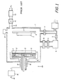
- Fig. 1 shows schematically an exemplar sputtering apparatus applicable for various materials.
- a sputtering chamber 1 the target 2 and the object 3 on which the thin film is to be grown are placed facing each other.
- the target is usually formed like a disk made of the material to be sputtered.
- the object 3 is held by an object holder 4, and the target 2 is supported by a target holder 5.
- the sputtering chamber 1 is evacuated by a cryogenic pump 6 and rotary pump 7. They are connected in cascade via a valve 8, but the rotary pump 7 can be also connected directly to the sputtering chamber 1 via another valve 9 for coarse evacuation.
- a gate valve 10 and a variable conductance valve 11, which controls the pumping speed are provided between the cryogenic pump 6 and the sputtering chamber 1 .
- the pressure in the sputtering chamber 1 is indicated on a manometer 12.
- An inert gas, argon for example, is fed through a mass flow controller 13 and an electromagnetic valve 14.
- the target holder 5 is water cooled with a water whose inlet and outlet are respectively shown by small arrows.
- the negative side of a high voltage source 15 is electrically connected to the target holder 5 and the target 2, while the positive side of the high voltage source 15 is grounded.
- a shield plate 16 which limits the glow discharge on the surface of the target 2, to prevent sputtering the other parts of the target holder.
- permanent magnets or electric magnets 17 are provided on the back side of the target holder 6.
- the target holder 5 is electrically isolated from the sputtering chamber 1 by an isolator 18.
- the pumping speed is the higher the better, to remove the impurity or residual gas and attain the high quality of the sputtered material.
- a high speed pump is equipped in ordinary sputtering apparatus, and inert gas is injected into the sputtering chamber.
- the pressure in the sputtering chamber should be in a proper range. Therefore, if the pump is operated in full speed, the pressure in the sputtering chamber becomes too low to maintain the glow discharge. So, the inert gas flow must be increased to balance with the pumping speed. This makes the gas consumption become very large, and decreases the activity of the cryogenic pump quickly. Therefore, the pump must be refreshed repeatedly, and the availability of the sputtering apparatus becomes low.
- the pumping speed and the flow rate of the inert gas are controlled by adjusting the variable conductance valve 11 so as to balance the pumping speed with the inert gas flow.
- the pumping speed is slowed down, therefore, the sputtered material suffers from contamination by the residual or adsorbed gas released in the sputtering chamber. This is especially undesirable for fabricating devices having very fine structures, such as LSI devices etc.
- the device life is decreased by the contamination, and the production yield of the device becomes unstable.
- the present invention intends to solve such difficulty.
- the inventor noticed that when the injection of the inert gas is pinched off after the discharge begins, the glow discharge is also quenched quickly. But if a small quantity of gas is injected continuously into the sputtering chamber, the glow discharge is sustained for a longer time period though the discharge current becomes small. But if the power source is operated in a constant power mode, the electric power supplied for the glow discharge from the power source does not decrease so rapidly, because though the discharge current decrease, the voltage goes up to maintain the discharge. Therefore, the electric sputtering can be carried on effectively for a larger period of time during the glow discharge is continuing. Throughout this period, the pump is working at high speed, so, the residual gas are removed quickly, and the contamination is suppressed. On the other hand, the total gas consumption is very small, because, during most of the time, the gas flow is suppressed to a low level.
- the gas discharge occurs at a relatively low voltage, few hundreds volts for example.
- the discharge does not occur unless a very high voltage is applied to cause a breakdown.
- the electric discharge can not occur at a low voltage of the first pressure range P1, but the discharge is substained when it is ignited in the first pressure range P1, and then the pressure is decreased to P2. But when the pressure further goes down below the second pressure range P2, the discharge is pinched off.
- Fig. 2 illustrates schematically a time chart for the inert gas flow injected into the sputtering chamber, and the variation of pressure in the sputtering chamber.
- abscissa shows time
- the left hand side ordinate indicates the flow rate of the gas injected into the sputtering chamber
- the right hand side ordinate indicates the pressure in the sputtering chamber.
- the pressure ranges P1, P2 depend on kind of the injected gas, magnetic field, shape of the target and object, and the applied voltage.
- the flow rate is kept to a high level F1 during a first time period T1.
- the high level flow rate F1 will be called first flow rate hereinafter.
- the pressure in the sputtering chamber goes up to the first pressure range P1, and the glow discharge is ignited.
- the low level flow rate F2 is called second flow rate herein after.
- the discharge is sustained to a pressure lower than the first pressure range P1. It should be noticed that, the discharge will be extinguished soon, if the gas flow is perfectly pinched off.
- the glow discharge is sustained for a longer time period. Since the second flow rate F2 is set to be lower than the pumping speed, the pressure will go down further. And if the pressure becomes lower than the second pressure range P2, the discharge will be extinguished final strictlyly. Before that, namely before the gas pressure is decreased to lower than the second pressure range P2, the gas is injected again with the first flow rate F1 as shown in Fig. 2, and the glow discharge is enhanced again.
- the period during which the gas is injected with the low flow rate (F2) and the glow discharge is sustained will be called second time period T2 hereinafter.
- the chamber, pumping speed, gas, target, and object are all determined to a specific value for each case by choosing the apparatus or design of the device.
- the first flow rate F1 will be obtained easily by gradually increasing the flow rate, and find out the starting point of the glow discharge.
- the first time period T1 is the smaller the better so long as the discharge is certainly started. Therefore, it is not difficult to find out these conditions.
- the remaining condition for the second flow rate F2 and the second period T2 can be also easily determined.
- the supplied power from the high voltage source is considered to be the power consumed by the glow discharge, and is used for bombarding the target to sputter it. If a constant DC power supply source is used, the voltage between the target and the object automatically increases when the pressure in the discharge chamber decreased, and the glow discharge is maintained. So, the output power is kept almost constant during the second period T2. But when the pressure becomes too low, the power supply source can not supply enough voltage, and the discharge current decreases quickly. This means the end of the second period T2. Too small power consumption is meaningless, because the sputtering rate becomes very small though the plasma is still sustained. Therefore, the glow discharge should be reinforced by injecting the gas before it becomes too weak. T2 is measured varying the second flow rate F2, and the optimum flow rate for elongating T2 is obtained. These conditions are all not so critical. Even if the plasma is extinguished, it does not harm any way.
- the second flow rate F2 should be far below the pumping speed. Since, if F2 becomes too large, F2 might balance with the pumping speed, and T2 may become very long. But this is not the solution, because the consumption of the gas increases and the refreshing period of the pump becomes short. Practically, the second flow rate F2 may be less than few tenth of the pumping speed. With such a small flow rate, sufficiently long period of T2 can be attained.
- the sputtering condition is easily determined for case by case. These conditions are not so critical.
- One example will be given for sputtering aluminum over a silicon substrate.
- Target aluminum disc including 1 weight % of silicon 290 mm in diameter
- Object silicon substrate 125 mm in diameter
- Distance between the target and the object about 55 mm
- Input power 10 kW DC.
- T1 0.2 - 0.5 sec
- T2 10 - 30 sec
- F1 80 - 100 sccm
- F2 20 - 50 sccm
- P1 2 - 5 mm Torr
- P1 0.5 - 2 mm Torr
- Pump speed 1,200 litter/min for argon.
- the unit sccm means a standard cubic cm per minute, that is a current flow rate (cc/min) measured in one atmospheric pressure at room temperature (20°C).
- the first period T1 is very short compared to the second period T2. So, the sputtering is done also under the low injection flow rate, and the pump is always operated fully. Accordingly, the contamination caused by the residual gas is perfectly avoided.
- Fig. 3 schematically illustrates a gas flow line system to realizes a flow of injection gas as shown in Fig. 2.
- This system is composed of two piping systems connected in parallel. One is a high flow rate line 19 and the other is a low flow rate line 20.
- the high flow rate line 19 comprises a first mass flow controller (MFC1) 21 and a first electromagnetic valve (V1) 22, while the low flow rate line 20 comprises a second mass flow controller (MFC2) 23 and a second electromagnetic valve (V2) 24.
- V1 and V2 are controlled by a controller (CON) 25.
- Such a gas flow line system is connected to the gas inlet 26 of the sputtering chamber shown in Fig. 1, replacing the electromagnetic valve 14 and the mass flow controller 13. It will be easily understood that the flow rate will be varied as shown in Fig. 2 by simply switching the electromagnetic valves V1 and V2 to alternately open respectively with a timing T1 and T2.
- Such control and programming for the controller 25 is a simple one, so further description is omitted for the sake of simplicity.
- Fig. 4 schematically illustrates another gas flow line system which is applicable for realizing the gas flow rate of Fig. 2.
- the high flow rate line 19 and the low flow rate line 20 are connected in series to each other. These lines respectively comprises the mass flow controllers MFC1 or MFC2, and the electromagnetic valves V1 or V2, and the flow rate through these lines 19 and 20 are adjusted to be F1 and F2 respectively.
- the low flow rate line 20 is provided with a bypass line 27 which comprises a third electromagnetic valve (V3) 28.
- the electromagnetic valves V1, V2 and V3 are controlled by a controller (not shown).
- Such gas flow line system is connected to the gas inlet 26 of the sputtering chamber shown in Fig. 1.
- the flow rate of the injection gas is not necessarily a pulse form as shown in Fig. 2 in order to perform the sputtering of the present invention.
- the spirit of the present invention is to perform the sputtering under a proper variation of the pressure in the sputtering chamber. If the pressure in the sputtering chamber is varied in a manner as shown in Fig. 2, similar effects as described before will be attained.
- Fig. 5 shows a flow rate of injection gas for a second embodiment of the present invention.
- the ordinate is the current flow rate
- the abscissa is time.
- the flow rate of the injection gas is varied rather gradually compared to the flow rate of Fig. 2.
- the gas flow is increased gradually, so the pressure in the sputtering chamber increases,and when the glow discharge is started or enhanced, the gas flow is decreased. So, the pressure in the sputtering chamber becomes low because the gas injection rate becomes lower than the pumping speed.
- the glow discharge is carried on mainly in a lower gas flow range.
- first flow rate F1 the higher flow rate of the injection gas by which the pressure in the sputtering chamber becomes the first pressure range P1
- second flow rate F2 the flow rate by which the pressure in the sputtering chamber decreases to the second pressure range P2.
- the value of F1 and F2 were respectively a constant value
- the category of F1 is expanded to a range of the flow rate by which the pressure in the sputtering chamber increases to the first pressure range P1.
- the category of F2 is also expanded to the flow rate by which the pressure in the sputtering chamber decreases to the second pressure range P2.
- a piezo gas flow valve for example is applicable for the electromagnetic valve 14. It varies the impedance for the gas flow by applied voltage.
- the conditions how to control the valve depends on the size of the sputtering chamber, pumping speed, kind of the gas, applied voltage and so on. But it will be understood that these conditions may be easily determined like a sim ilar manner to the first embodiment described before.
- the conditions are not critical, and various modifications may be possible. For example, the increment and decrement of the flow rate curve of Fig. 5 may be changed in various ways.
- the flow rate is increased from 20 sccm to 90 sccm in 5 - 10 sec.
- the glow discharge is ignited at a flow rate of about 80 sccm. This means that the pressure in the sputtering chamber reached to the first pressure range P1 at this flow rate.
- the flow rate is turned to decrease, and in 20 - 30 sec the flow rate is decreased to 20 sccm, then it is again increased. Such a variation of flow rate is repeated during the sputtering operation.
- a modification of the second embodiment can be easily derived.
- the flow rate is not necessarily increased until the pressure in the sputtering chamber increases to the first pressure range P1, that corresponds to 80 sccm in current flow in Fig. 5.
- the flow rate may be decreased before the pressure reaches the first pressure range P1.
- the flow rate corresponding the turning point A in Fig. 5 will be called third flow rate F3 hereinafter.
- the flow rate is again turned to increase.
- the flow rate at the lower turning point B is called fourth flow rate F4.
- the third flow rate F3 corresponds to a flow rate by which the pressure in the sputtering chamber goes up just below P1.
- the fourth flow rate F4 corresponds to a flow rate by which the pressure goes down just above the bottom of the second pressure range P2. They must be determined case by case.
- the values of F3 and F4 are not so critical. It will easily for the one skilled in the art to determine these values like a similar manner to finding out the value of F2 as described with respect to the first embodiment.
- the injection gas flow is controlled to go up and down between F3 and F4.
- the total gas consumption is further decreased compared to that of the second embodiment, and hence, the recycle period of the evacuation pump is further elongated.
- the evacuation pump for the sputtering chamber is operated at full speed during the sputtering process. So, the residual gas in the chamber is removed away quickly, and the contamination caused by such residual gas is avoided. Therefore, a fine and high grade sputtered film can be produced. While the flow rate of the injection gas is reduced, the consumption of the gas is saved, and the recycling period of the cryogenic pump can be elongated, so, the availability of the sputtering apparatus is improved.
- the present method of sputtering has additional effects that the sputtering voltage is increased in average, so the sputtering rate is increased compared to prior art sputtering methods. Further, the sputtered film has a good coverage on an object having steps on its surface. This is considered to be due to the fact that the sputtering is performed under a lower gas pressure, so, the mean free pass of the sputtered particle is increased. This enables the sputtered particle to fly along the electric lines of force which is perpendicular to the surface of the object.
- the description has been done referring to a method for forming a thin film especially aluminum film over a semiconductor substrate.
- the present invention is not restricted to such an application. It can be applied for fabricating various objects such as semiconductor devices, thin film circuits or devices, optical equipments and so on.
- the sputtered material also can be varied in variety, such as metal, dielectrics, semiconductors and so on.
Landscapes
- Chemical & Material Sciences (AREA)
- Chemical Kinetics & Catalysis (AREA)
- Engineering & Computer Science (AREA)
- Materials Engineering (AREA)
- Mechanical Engineering (AREA)
- Metallurgy (AREA)
- Organic Chemistry (AREA)
- Physical Vapour Deposition (AREA)
- Internal Circuitry In Semiconductor Integrated Circuit Devices (AREA)
- Physical Deposition Of Substances That Are Components Of Semiconductor Devices (AREA)
Applications Claiming Priority (2)
| Application Number | Priority Date | Filing Date | Title |
|---|---|---|---|
| JP63141507A JPH01312851A (ja) | 1988-06-10 | 1988-06-10 | 半導体装置の製造方法 |
| JP141507/88 | 1988-06-10 |
Publications (2)
| Publication Number | Publication Date |
|---|---|
| EP0345487A1 true EP0345487A1 (de) | 1989-12-13 |
| EP0345487B1 EP0345487B1 (de) | 1994-02-16 |
Family
ID=15293566
Family Applications (1)
| Application Number | Title | Priority Date | Filing Date |
|---|---|---|---|
| EP89108689A Expired - Lifetime EP0345487B1 (de) | 1988-06-10 | 1989-05-13 | Sputterverfahren zur Erzeugung einer Dünnschicht |
Country Status (5)
| Country | Link |
|---|---|
| US (1) | US5049251A (de) |
| EP (1) | EP0345487B1 (de) |
| JP (1) | JPH01312851A (de) |
| KR (1) | KR930001501B1 (de) |
| DE (1) | DE68913077T2 (de) |
Cited By (3)
| Publication number | Priority date | Publication date | Assignee | Title |
|---|---|---|---|---|
| GB2264718A (en) * | 1992-03-04 | 1993-09-08 | Univ Hull | Vapour deposited coatings having at least three transitions in structure |
| EP2963149A4 (de) * | 2013-02-28 | 2016-10-12 | Ayabo Corp | Gepulste sputtervorrichtung und gepulstes sputterverfahren |
| CN109037117A (zh) * | 2018-09-04 | 2018-12-18 | 长江存储科技有限责任公司 | 压力调整装置 |
Families Citing this family (36)
| Publication number | Priority date | Publication date | Assignee | Title |
|---|---|---|---|---|
| KR100333237B1 (ko) * | 1993-10-29 | 2002-09-12 | 어플라이드 머티어리얼스, 인코포레이티드 | 플라즈마에칭챔버내에서오염물질을감소시키는장치및방법 |
| US6465043B1 (en) * | 1996-02-09 | 2002-10-15 | Applied Materials, Inc. | Method and apparatus for reducing particle contamination in a substrate processing chamber |
| US5902494A (en) * | 1996-02-09 | 1999-05-11 | Applied Materials, Inc. | Method and apparatus for reducing particle generation by limiting DC bias spike |
| US5667645A (en) * | 1996-06-28 | 1997-09-16 | Micron Technology, Inc. | Method of sputter deposition |
| JP3429957B2 (ja) * | 1996-08-28 | 2003-07-28 | 松下電器産業株式会社 | スパッタリング方法及び装置 |
| US6013159A (en) * | 1997-11-16 | 2000-01-11 | Applied Materials, Inc. | Particle trap in a magnetron sputtering chamber |
| US6174811B1 (en) * | 1998-12-02 | 2001-01-16 | Applied Materials, Inc. | Integrated deposition process for copper metallization |
| US6733513B2 (en) * | 1999-11-04 | 2004-05-11 | Advanced Bioprosthetic Surfaces, Ltd. | Balloon catheter having metal balloon and method of making same |
| US6458251B1 (en) * | 1999-11-16 | 2002-10-01 | Applied Materials, Inc. | Pressure modulation method to obtain improved step coverage of seed layer |
| US7736687B2 (en) | 2006-01-31 | 2010-06-15 | Advance Bio Prosthetic Surfaces, Ltd. | Methods of making medical devices |
| US7235092B2 (en) * | 1999-11-19 | 2007-06-26 | Advanced Bio Prosthetic Surfaces, Ltd. | Guidewires and thin film catheter-sheaths and method of making same |
| US8458879B2 (en) | 2001-07-03 | 2013-06-11 | Advanced Bio Prosthetic Surfaces, Ltd., A Wholly Owned Subsidiary Of Palmaz Scientific, Inc. | Method of fabricating an implantable medical device |
| US10172730B2 (en) | 1999-11-19 | 2019-01-08 | Vactronix Scientific, Llc | Stents with metallic covers and methods of making same |
| US6849085B2 (en) | 1999-11-19 | 2005-02-01 | Advanced Bio Prosthetic Surfaces, Ltd. | Self-supporting laminated films, structural materials and medical devices manufactured therefrom and method of making same |
| US6936066B2 (en) * | 1999-11-19 | 2005-08-30 | Advanced Bio Prosthetic Surfaces, Ltd. | Complaint implantable medical devices and methods of making same |
| US7300457B2 (en) | 1999-11-19 | 2007-11-27 | Advanced Bio Prosthetic Surfaces, Ltd. | Self-supporting metallic implantable grafts, compliant implantable medical devices and methods of making same |
| US6379383B1 (en) | 1999-11-19 | 2002-04-30 | Advanced Bio Prosthetic Surfaces, Ltd. | Endoluminal device exhibiting improved endothelialization and method of manufacture thereof |
| US6537310B1 (en) | 1999-11-19 | 2003-03-25 | Advanced Bio Prosthetic Surfaces, Ltd. | Endoluminal implantable devices and method of making same |
| US7195641B2 (en) | 1999-11-19 | 2007-03-27 | Advanced Bio Prosthetic Surfaces, Ltd. | Valvular prostheses having metal or pseudometallic construction and methods of manufacture |
| US6312568B2 (en) | 1999-12-07 | 2001-11-06 | Applied Materials, Inc. | Two-step AIN-PVD for improved film properties |
| JP3376998B2 (ja) | 2000-03-08 | 2003-02-17 | 日本電気株式会社 | 半導体記憶装置 |
| US6695865B2 (en) | 2000-03-20 | 2004-02-24 | Advanced Bio Prosthetic Surfaces, Ltd. | Embolic protection device |
| US9566148B2 (en) | 2000-05-12 | 2017-02-14 | Vactronix Scientific, Inc. | Self-supporting laminated films, structural materials and medical devices manufactured therefrom and methods of making same |
| WO2002038080A2 (en) | 2000-11-07 | 2002-05-16 | Advanced Bio Prosthetic Surfaces, Ltd. | Endoluminal stent, self-fupporting endoluminal graft and methods of making same |
| AU2003270817B2 (en) | 2002-09-26 | 2009-09-17 | Vactronix Scientific, Llc | High strength vacuum deposited nitionol alloy films, medical thin film graft materials and method of making same |
| US20040161536A1 (en) * | 2003-02-14 | 2004-08-19 | Applied Materials, Inc. | Method for depositing a low-k material having a controlled thickness range |
| CN101005812A (zh) | 2003-05-07 | 2007-07-25 | 先进生物假体表面有限公司 | 可植入性金属移植物及其制造方法 |
| US7300558B2 (en) * | 2003-10-21 | 2007-11-27 | Seagate Technology Llc | Rapid cycle time gas burster |
| KR100599924B1 (ko) * | 2004-03-26 | 2006-07-12 | 어플라이드 필름스 게엠베하 운트 컴퍼니 카게 | 반응성 스퍼터링용 장치 |
| DE102004014855A1 (de) * | 2004-03-26 | 2004-10-21 | Applied Films Gmbh & Co. Kg | Einrichtung zum reaktiven Sputtern |
| KR101174146B1 (ko) * | 2005-06-28 | 2012-08-14 | 엘지디스플레이 주식회사 | 스퍼터링 장치 |
| US9399812B2 (en) * | 2011-10-11 | 2016-07-26 | Applied Materials, Inc. | Methods of preventing plasma induced damage during substrate processing |
| DE102015117448A1 (de) * | 2015-09-02 | 2017-03-02 | Von Ardenne Gmbh | Verfahren und Prozessieranordnung |
| CN113412341B (zh) * | 2019-02-11 | 2024-11-01 | 应用材料公司 | 在脉冲式pvd中通过等离子体改性从晶片移除颗粒的方法 |
| US11676632B2 (en) * | 2019-12-26 | 2023-06-13 | Resonac Corporation | Magnetic recording medium, method of manufacturing magnetic recording medium and magnetic storage device |
| DE102023124377A1 (de) * | 2023-09-11 | 2025-03-13 | Eltro Gmbh | Verfahren zur Oberflächenbeschichtung nach dem Sputterprinzip |
Citations (2)
| Publication number | Priority date | Publication date | Assignee | Title |
|---|---|---|---|---|
| US4428812A (en) * | 1983-04-04 | 1984-01-31 | Borg-Warner Corporation | Rapid rate reactive sputtering of metallic compounds |
| US4440618A (en) * | 1982-03-19 | 1984-04-03 | Anelva Corporation | Gas discharge device comprising a pressure controller for controlling a pressure over a wide range |
Family Cites Families (4)
| Publication number | Priority date | Publication date | Assignee | Title |
|---|---|---|---|---|
| JPS5729577A (en) * | 1980-07-30 | 1982-02-17 | Anelva Corp | Automatic continuous sputtering apparatus |
| JP2515977B2 (ja) * | 1986-03-11 | 1996-07-10 | アネルバ株式会社 | スパツタ装置 |
| GB8609619D0 (en) * | 1986-04-19 | 1986-05-21 | Procal Analytics | Gas analysis |
| JPS63259076A (ja) * | 1987-04-15 | 1988-10-26 | Hitachi Ltd | スパツタリング装置のプラズマ起動方法 |
-
1988
- 1988-06-10 JP JP63141507A patent/JPH01312851A/ja active Granted
-
1989
- 1989-05-13 EP EP89108689A patent/EP0345487B1/de not_active Expired - Lifetime
- 1989-05-13 DE DE68913077T patent/DE68913077T2/de not_active Expired - Fee Related
- 1989-06-07 US US07/362,712 patent/US5049251A/en not_active Expired - Fee Related
- 1989-06-10 KR KR1019890007998A patent/KR930001501B1/ko not_active Expired - Fee Related
Patent Citations (2)
| Publication number | Priority date | Publication date | Assignee | Title |
|---|---|---|---|---|
| US4440618A (en) * | 1982-03-19 | 1984-04-03 | Anelva Corporation | Gas discharge device comprising a pressure controller for controlling a pressure over a wide range |
| US4428812A (en) * | 1983-04-04 | 1984-01-31 | Borg-Warner Corporation | Rapid rate reactive sputtering of metallic compounds |
Cited By (5)
| Publication number | Priority date | Publication date | Assignee | Title |
|---|---|---|---|---|
| GB2264718A (en) * | 1992-03-04 | 1993-09-08 | Univ Hull | Vapour deposited coatings having at least three transitions in structure |
| GB2264718B (en) * | 1992-03-04 | 1995-04-26 | Univ Hull | Coatings produced by vapour deposition |
| EP2963149A4 (de) * | 2013-02-28 | 2016-10-12 | Ayabo Corp | Gepulste sputtervorrichtung und gepulstes sputterverfahren |
| CN109037117A (zh) * | 2018-09-04 | 2018-12-18 | 长江存储科技有限责任公司 | 压力调整装置 |
| CN109037117B (zh) * | 2018-09-04 | 2023-11-28 | 长江存储科技有限责任公司 | 压力调整装置 |
Also Published As
| Publication number | Publication date |
|---|---|
| KR910002029A (ko) | 1991-01-31 |
| JPH01312851A (ja) | 1989-12-18 |
| JPH0577329B2 (de) | 1993-10-26 |
| US5049251A (en) | 1991-09-17 |
| KR930001501B1 (ko) | 1993-03-02 |
| DE68913077D1 (de) | 1994-03-24 |
| DE68913077T2 (de) | 1994-06-01 |
| EP0345487B1 (de) | 1994-02-16 |
Similar Documents
| Publication | Publication Date | Title |
|---|---|---|
| EP0345487B1 (de) | Sputterverfahren zur Erzeugung einer Dünnschicht | |
| US5830330A (en) | Method and apparatus for low pressure sputtering | |
| US6872289B2 (en) | Thin film fabrication method and thin film fabrication apparatus | |
| US5223457A (en) | High-frequency semiconductor wafer processing method using a negative self-bias | |
| KR100886273B1 (ko) | 플라즈마 처리 장치 및 플라즈마 처리 방법 | |
| US4309266A (en) | Magnetron sputtering apparatus | |
| CN1800441A (zh) | 等离子体增强薄膜沉积方法及装置 | |
| EP1044459A1 (de) | Plasmavorrichtung mit einem mit einer spannungsquelle verbundenen metallteil, das zwischen einer rf-plasma-anregungsquelle und dem plasma angeordnet ist | |
| CN100414672C (zh) | 等离子体处理方法及等离子体处理装置 | |
| JP2023546468A (ja) | 酸化物薄膜の製造方法 | |
| EP0760160A1 (de) | Sanfte plasmazuendung in plasmabearbeitungskammern | |
| JPS6131186B2 (de) | ||
| EP0594328B1 (de) | Methode zur Steuerung von Plasmaverfahren | |
| US20010017190A1 (en) | Apparatus of processing a sample surface and method thereof | |
| JP3429957B2 (ja) | スパッタリング方法及び装置 | |
| KR101191698B1 (ko) | 저압력 플라즈마를 점화시키는 방법 및 장치 | |
| US3528902A (en) | Method of producing thin films by sputtering | |
| JPH09217171A (ja) | Ito透明導電膜の作製方法 | |
| US6342139B1 (en) | Sputtering system | |
| JPH024674B2 (de) | ||
| CN116802336B (zh) | 氮化硅膜的成膜方法、成膜装置及氮化硅膜 | |
| TWI913636B (zh) | 成膜方法 | |
| US6176980B1 (en) | Sputtering method and apparatus | |
| JP2000160337A (ja) | マグネトロンスパッタ装置 | |
| JPH02205674A (ja) | マグネトロンスパッタリング装置 |
Legal Events
| Date | Code | Title | Description |
|---|---|---|---|
| PUAI | Public reference made under article 153(3) epc to a published international application that has entered the european phase |
Free format text: ORIGINAL CODE: 0009012 |
|
| AK | Designated contracting states |
Kind code of ref document: A1 Designated state(s): DE FR GB |
|
| 17P | Request for examination filed |
Effective date: 19891205 |
|
| 17Q | First examination report despatched |
Effective date: 19920825 |
|
| GRAA | (expected) grant |
Free format text: ORIGINAL CODE: 0009210 |
|
| AK | Designated contracting states |
Kind code of ref document: B1 Designated state(s): DE FR GB |
|
| REF | Corresponds to: |
Ref document number: 68913077 Country of ref document: DE Date of ref document: 19940324 |
|
| ET | Fr: translation filed | ||
| PLBE | No opposition filed within time limit |
Free format text: ORIGINAL CODE: 0009261 |
|
| STAA | Information on the status of an ep patent application or granted ep patent |
Free format text: STATUS: NO OPPOSITION FILED WITHIN TIME LIMIT |
|
| 26N | No opposition filed | ||
| PGFP | Annual fee paid to national office [announced via postgrant information from national office to epo] |
Ref country code: GB Payment date: 19970506 Year of fee payment: 9 |
|
| PGFP | Annual fee paid to national office [announced via postgrant information from national office to epo] |
Ref country code: FR Payment date: 19970513 Year of fee payment: 9 |
|
| PGFP | Annual fee paid to national office [announced via postgrant information from national office to epo] |
Ref country code: DE Payment date: 19970516 Year of fee payment: 9 |
|
| PG25 | Lapsed in a contracting state [announced via postgrant information from national office to epo] |
Ref country code: GB Free format text: LAPSE BECAUSE OF NON-PAYMENT OF DUE FEES Effective date: 19980513 |
|
| PG25 | Lapsed in a contracting state [announced via postgrant information from national office to epo] |
Ref country code: FR Free format text: LAPSE BECAUSE OF NON-PAYMENT OF DUE FEES Effective date: 19980531 |
|
| GBPC | Gb: european patent ceased through non-payment of renewal fee |
Effective date: 19980513 |
|
| PG25 | Lapsed in a contracting state [announced via postgrant information from national office to epo] |
Ref country code: DE Free format text: LAPSE BECAUSE OF NON-PAYMENT OF DUE FEES Effective date: 19990302 |
|
| REG | Reference to a national code |
Ref country code: FR Ref legal event code: ST |