EP0345037A2 - Gerät zur Aufnahme von digitalen Signalen - Google Patents
Gerät zur Aufnahme von digitalen Signalen Download PDFInfo
- Publication number
- EP0345037A2 EP0345037A2 EP89305473A EP89305473A EP0345037A2 EP 0345037 A2 EP0345037 A2 EP 0345037A2 EP 89305473 A EP89305473 A EP 89305473A EP 89305473 A EP89305473 A EP 89305473A EP 0345037 A2 EP0345037 A2 EP 0345037A2
- Authority
- EP
- European Patent Office
- Prior art keywords
- recording
- digital signal
- signal
- recording apparatus
- erasure
- Prior art date
- Legal status (The legal status is an assumption and is not a legal conclusion. Google has not performed a legal analysis and makes no representation as to the accuracy of the status listed.)
- Granted
Links
Images


Classifications
-
- G—PHYSICS
- G11—INFORMATION STORAGE
- G11B—INFORMATION STORAGE BASED ON RELATIVE MOVEMENT BETWEEN RECORD CARRIER AND TRANSDUCER
- G11B20/00—Signal processing not specific to the method of recording or reproducing; Circuits therefor
- G11B20/10—Digital recording or reproducing
-
- G—PHYSICS
- G11—INFORMATION STORAGE
- G11B—INFORMATION STORAGE BASED ON RELATIVE MOVEMENT BETWEEN RECORD CARRIER AND TRANSDUCER
- G11B15/00—Driving, starting or stopping record carriers of filamentary or web form; Driving both such record carriers and heads; Guiding such record carriers or containers therefor; Control thereof; Control of operating function
- G11B15/02—Control of operating function, e.g. switching from recording to reproducing
- G11B15/12—Masking of heads; circuits for Selecting or switching of heads between operative and inoperative functions or between different operative functions or for selection between operative heads; Masking of beams, e.g. of light beams
- G11B15/125—Masking of heads; circuits for Selecting or switching of heads between operative and inoperative functions or between different operative functions or for selection between operative heads; Masking of beams, e.g. of light beams conditioned by the operating function of the apparatus
-
- G—PHYSICS
- G11—INFORMATION STORAGE
- G11B—INFORMATION STORAGE BASED ON RELATIVE MOVEMENT BETWEEN RECORD CARRIER AND TRANSDUCER
- G11B20/00—Signal processing not specific to the method of recording or reproducing; Circuits therefor
- G11B20/10—Digital recording or reproducing
- G11B20/14—Digital recording or reproducing using self-clocking codes
- G11B20/1403—Digital recording or reproducing using self-clocking codes characterised by the use of two levels
- G11B20/1407—Digital recording or reproducing using self-clocking codes characterised by the use of two levels code representation depending on a single bit, i.e. where a one is always represented by a first code symbol while a zero is always represented by a second code symbol
- G11B20/1419—Digital recording or reproducing using self-clocking codes characterised by the use of two levels code representation depending on a single bit, i.e. where a one is always represented by a first code symbol while a zero is always represented by a second code symbol to or from biphase level coding, i.e. to or from codes where a one is coded as a transition from a high to a low level during the middle of a bit cell and a zero is encoded as a transition from a low to a high level during the middle of a bit cell or vice versa, e.g. split phase code, Manchester code conversion to or from biphase space or mark coding, i.e. to or from codes where there is a transition at the beginning of every bit cell and a one has no second transition and a zero has a second transition one half of a bit period later or vice versa, e.g. double frequency code, FM code
-
- G—PHYSICS
- G11—INFORMATION STORAGE
- G11B—INFORMATION STORAGE BASED ON RELATIVE MOVEMENT BETWEEN RECORD CARRIER AND TRANSDUCER
- G11B27/00—Editing; Indexing; Addressing; Timing or synchronising; Monitoring; Measuring tape travel
- G11B27/02—Editing, e.g. varying the order of information signals recorded on, or reproduced from, record carriers
- G11B27/031—Electronic editing of digitised analogue information signals, e.g. audio or video signals
- G11B27/036—Insert-editing
-
- G—PHYSICS
- G11—INFORMATION STORAGE
- G11B—INFORMATION STORAGE BASED ON RELATIVE MOVEMENT BETWEEN RECORD CARRIER AND TRANSDUCER
- G11B5/00—Recording by magnetisation or demagnetisation of a record carrier; Reproducing by magnetic means; Record carriers therefor
- G11B5/02—Recording, reproducing, or erasing methods; Read, write or erase circuits therefor
- G11B5/024—Erasing
-
- G—PHYSICS
- G11—INFORMATION STORAGE
- G11B—INFORMATION STORAGE BASED ON RELATIVE MOVEMENT BETWEEN RECORD CARRIER AND TRANSDUCER
- G11B5/00—Recording by magnetisation or demagnetisation of a record carrier; Reproducing by magnetic means; Record carriers therefor
- G11B5/02—Recording, reproducing, or erasing methods; Read, write or erase circuits therefor
- G11B5/09—Digital recording
-
- G—PHYSICS
- G11—INFORMATION STORAGE
- G11B—INFORMATION STORAGE BASED ON RELATIVE MOVEMENT BETWEEN RECORD CARRIER AND TRANSDUCER
- G11B5/00—Recording by magnetisation or demagnetisation of a record carrier; Reproducing by magnetic means; Record carriers therefor
- G11B5/48—Disposition or mounting of heads or head supports relative to record carriers ; arrangements of heads, e.g. for scanning the record carrier to increase the relative speed
- G11B5/52—Disposition or mounting of heads or head supports relative to record carriers ; arrangements of heads, e.g. for scanning the record carrier to increase the relative speed with simultaneous movement of head and record carrier, e.g. rotation of head
- G11B5/53—Disposition or mounting of heads on rotating support
- G11B5/531—Disposition of more than one recording or reproducing head on support rotating cyclically around an axis
-
- G—PHYSICS
- G11—INFORMATION STORAGE
- G11B—INFORMATION STORAGE BASED ON RELATIVE MOVEMENT BETWEEN RECORD CARRIER AND TRANSDUCER
- G11B2220/00—Record carriers by type
- G11B2220/90—Tape-like record carriers
-
- G—PHYSICS
- G11—INFORMATION STORAGE
- G11B—INFORMATION STORAGE BASED ON RELATIVE MOVEMENT BETWEEN RECORD CARRIER AND TRANSDUCER
- G11B27/00—Editing; Indexing; Addressing; Timing or synchronising; Monitoring; Measuring tape travel
- G11B27/02—Editing, e.g. varying the order of information signals recorded on, or reproduced from, record carriers
- G11B27/031—Electronic editing of digitised analogue information signals, e.g. audio or video signals
- G11B27/032—Electronic editing of digitised analogue information signals, e.g. audio or video signals on tapes
Definitions
- This invention relates to a digital signal recording apparatus for recording an input signal on a recording medium in the form of pulse train recording.
- VTRs video tape recorders
- signals are recorded obliquely on a magnetic tape by plural recording magnetic heads provided at predetermined positions on a rotational drum.
- an erasure magnetic head is provided to a rotary drum at a position preceding the recording magnetic head for accurately tracing the recording track and signal re-recording is performed by the recording magnetic head after flying erasure previously performed by the erasure magnetic head for a period corresponding to the re-recording period.
- the flying erasure is occasionally performed for satisfactory signal re-recording during the editing.
- a separate erasure control circuit for supplying the electrical circuit to the erasure magnetic head in timing with the re-recording period or the rotary transformer for transmitting control signals are necessary to provide besides the recording system. In addition, the power consumption is increased.
- the recording magnetic head and the erasure magnetic head are provided in proximity to each other and control means for commonly controling the operational timing of each of these magnetic heads is realized by a circuit of a simplified structure with a high power efficiency for overcoming the above described in conveniences.
- an erasure magnetic head is provided to the rotary drum and the recording track is erased by flying erasure by the erasure magnetic head to effect satisfactory signal recording during editing.
- flying erasure is perfomred, not only a separate erasure control circuit for supplying the current to the erasure magnetic head in timing with the re-recording period, but a rotary transformer for transmitting the erasure control signals, are necessitated, while the power consumption is increased.
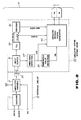
- Fig. 2 is a block diagram showing the general arrangement of an erasure/recording system for an erasure magnetic head H E and a recording magnetic head H R for one channel of a digital VTR to which the present invention is applied.
- the erasure magnetic head H E and the recording magnetic head H R are provided integrally with a predetermined distance therebetween which is short enough not to affect these heads H E or H R or a magnetic tape TP.
- These magnetic heads H E and H R are mounted at predetermined positioins on the outer periphery of a rotary drum, not shown, so as to be both rotated in physical contact with the magnetic tape TP, and are adapted to erase the recording track formed by the recording magnetic head H R by the erasure head H E preceding the recording magnetic head H R .
- This integral type erasure/recording magnetic head may be produced by bonding the heads H E and H R to each other or by providing a central magnetic body between the heads H E and H R .
- an internal circuit 30 which is electrically connected with an external circuit 10 via a rotary transformer 20.
- the external circuit 10 is provided with an encoder 11 supplied with clocks CLOCK of a predetermined period and recording data DATA from a signal generator, not shown, of a preceding stage, and an amplitude variable circuit 12 supplied with a recording current control signal ICO and a record operation command signal or record enable signal R E from a system controller, not shown.
- the encoder 11 phase encodes the recording data DATA based on the clocks CLOCK to modulate the data into data having the waveform suited for transmission by the rotary transformer 20.
- the amplitude variable circuit 12 converts the signals supplied from the encoder 11 into signals having the amplitude corresponding to the record current control signal ICO and supplies these signals to the rotary transformer 20 when the record operation is commanded by the record enable signal R E .
- the signals supplied to this rotary transformer 20 are transmitted to the internal circuit 30 in which it is supplied via an input buffer circuit 31 to a phase locked loop (PLL) circuit 32 and an amplitude detector 34.
- the PLL circuit 32 takes out phase encoding or PE record data and clocks CLOCK from the output signals of the input buffer circuit 31 to supply these data and clocks to a decoder 33.
- the decoder 33 converts the PE record data into non-return to zero or NRZ record data, based on the aforementioned clocks CLOCK.
- the amplitude detector 34 also generates the record current control signals ICO in accordance with the amplitude of the output signals from the buffer circuit 31 to supply these control signals to a threshold value detector 35.
- the detector 35 generates the record enable signal RE from the threshold value of the record current control signal ICO.
- the clocks CLOCK, NRZ record data, record current control signals ICO and the record enable signals RE, outputted respectively from the PLL circuit 32, decoder 33, amplitude detector 34 and the threshold value detector 35, are supplied to an erasure/recording signal generator 40.
- the current for driving the circuitry in the interior circuit 30 of the rotary drum 30 and the magnetic heads H E and H R is supplied from the slip ring or a power rotary transformer, not shown.
- the internal circuit 30 can be formed without using the PLL circuit 32 if the clock CLOCK and the record data are adapted to be transmitted by separate rotary transformers.
- the erasure/recording signal generator 40 is generally composed of a logic circuit formed by an emitter coupled logic or ECL performing an operation represented by two buffers 41, 42 each having an inverting output terminal, two AND circuits 43, 44 and a buffer 45, and three serially connected pairs of NPN transistors 46, 47; 48, 49; 50, 51.
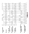
- the NRZ record data going to a high level or H level with the data "1" and to a low level or L level with the data "0" as shown at A in Fig. 3 are supplied to a data input terminal 52.
- the clocks CLOCK having one data length of the above described NRZ recording data as one period are also supplied to a clock input terminal 53, as shown at B in Fig. 3.
- the NRZ recording data are supplied via the buffer 41 so that the non-inverted data thereof are supplied to the AND circuit 43 while the inverted data thereof are supplied to the AND circuit 44.
- the clocks CLOCK supplied to the clock input terminal 53 are supplied via the buffer 42 so that the inverted data thereof are supplied to each of the logic elements 43, 44.
- These AND circuits 43, 44 from logical product data from the NRZ record data and the clocks CLOCK supplied to their input terminals, as shown at C or D in Fig. 3 and supply the logical product data to the base of the transistors 49, 50. From the inverting output terminal of the buffer 42, the inverted data of the clocks CLOCK as shown at E in Fig. 3 are outputted and supplied to the base of the transistor 51 bia buffer 45 at the same timing as the output data of the AND circuits 43, 44.
- the coil W R of the recording magnetic head H R has its one end connected via transistor 46 to the collector of the transistor 49, while having its other end connected via transistor 47 to the collector of transistor 50 and its neutral point to a positive voltage terminal Vcc of, for example, +10 V.
- the coil W E of the erasure magnetic head H E has its one end connected to the positive voltage terminal Vcc and grounded via a decoupling capacitor 56, while having its other end connected to the collector of the transistor 51 via transistor 48.
- the coil W E of the erasure magnetic head H E has its both ends connected via capacitor 57.
- the base of the transistors 46, 47 and 48 are connected in common.
- Each of the transistors 49, 50 and 51 has its emitter connected in common to a record current source 59 which in turn has its current value controlled in accordance with the record current control signal ICO supplied via the record current control signal input terminal 55.
- a recording current source 59 To this recording current source 59 is connected a negative voltage terminal V EE of, for example, -5V, via a switching circuit 58. This switching circuit is closed when a record operation is commanded by the above record operation command signal or record enable signal R E supplied to the switching circuit via record operation command signal input terminal 54.
- an electric current controlled to an optimum value in accordance with the above record current control signal ICO flows from the emitters of the transistors 49, 50 and 51.
- transistor 49 is turned on when the output data from the AND circuit 43 shown an C in Fig. 3 is "H", that is, during the period when the above NRZ record data is “1” and the clock is “H".
- transistor 50 is turned on when the output data of the AND circuit 44 supplied to the base of transistor 50 as shown at D in Fig. 3 is “H”, that is, during the period when the above NZR record data is "0" and the above clock is "H”
- transistor 51 is turned on when the inverted data of the clock CLOCK supplied to the base of transistor 51 as shown at E in Fig. 3 is "H", that is, when the above clock is "L".
- a pulse train recording is achieved on the magnetic tape TP by a magnetic field produced in the recording magnetic head H R by this recording current.
- an a.c. erasure is performed by an a.c. erasure current which is formed by the above parallel resonance circuit from the recording current supplied at each period of the reference level "Z", so that the pulse train recording and the a.c. erasure may be realized with the power consumption about equal to that in the case of the conventional NZR recording and without employing complicated circuits.
- Fig. 4 statistically shows the status of the errors produced in the data recorded and reproduced in the 4:2:2 digital VTR provided with four channels of the above described erasure and recording system.
- the ordinate denotes the number of times of errors in second and the abscissa the error length.
- the number of times of errors caused in the data obtained by a.c. erasure followed by pulse train recording by a digital VTR to which the present invention is applied, as shown by a solid line A is significantly smaller than that of errors in the case of a SMPTE model as shown by a broken line B.
- the transistors 49, 50 and 51 are turned on alternately, so that the current shown by the arrow I H , I L or I E is supplied from one of these transistors to the above recording current source 59. These currents are supplied via transistors 46, 47 and 48 to the transistors 49, 50 and 51, so that, even when the currents of a larger amplitude are supplied to the collectors of the transistors 46, 47 and 48 during different period, the effects on the transistors 49, 50 and 51 may be reduced.
- the recording tracks formed by the recording magnetic head H R are subjected to rotational erasure by an a.c. magnetic field prior to pulse train recording by the erasure magnetic head H E provided integrally with the recording magnetic head H R .
- the recording data may be recorded on the magnetic tape TP with a good S/N ratio not only during the ordinary recording but also during editing, so that the errors at the time of the reproduction may be reduced significantly.
- the erasure magnetic head H E is disposed at a sufficiently short distance from the recording magnetic head H R and the erasure current is adapted to flow in the coil W E during the time when the recording magnetic head H R is performing the recording operation, so that the complex circuitry for timing or a rotary transformer for control signal transmission may be dispensed with.
- the recording current during the reference level period of the pulse train recording is used as the erasure current supplied to the erasure magnetic head H E , so that the recording current source 59 provided for driving the recording magnetic head H R may be used simultaneously as the current source for the recording current.
- the pulse train recording and the a.c. erasure may be achieved with the power consumption about equal to that in the case of the conventional NRZ recording which is not the pulse train recording.
- phase distortions such as peak shifts caused in the conventional NRZ recording may be reduced and the compensation circuits therefore may be dispensed with.
- the result is that the adjustment point is solely the record current value by the record current control signal ICO so that the adjustment operation is facilitated.
Landscapes
- Engineering & Computer Science (AREA)
- Signal Processing (AREA)
- Multimedia (AREA)
- Digital Magnetic Recording (AREA)
Applications Claiming Priority (2)
| Application Number | Priority Date | Filing Date | Title |
|---|---|---|---|
| JP63133922A JP2606284B2 (ja) | 1988-05-31 | 1988-05-31 | 信号記録装置 |
| JP133922/88 | 1988-05-31 |
Publications (3)
| Publication Number | Publication Date |
|---|---|
| EP0345037A2 true EP0345037A2 (de) | 1989-12-06 |
| EP0345037A3 EP0345037A3 (de) | 1992-01-08 |
| EP0345037B1 EP0345037B1 (de) | 1994-11-02 |
Family
ID=15116224
Family Applications (1)
| Application Number | Title | Priority Date | Filing Date |
|---|---|---|---|
| EP89305473A Expired - Lifetime EP0345037B1 (de) | 1988-05-31 | 1989-05-31 | Gerät zur Aufnahme von digitalen Signalen |
Country Status (6)
| Country | Link |
|---|---|
| US (1) | US5070416A (de) |
| EP (1) | EP0345037B1 (de) |
| JP (1) | JP2606284B2 (de) |
| KR (1) | KR0161677B1 (de) |
| CA (1) | CA1322403C (de) |
| DE (1) | DE68919129T2 (de) |
Cited By (5)
| Publication number | Priority date | Publication date | Assignee | Title |
|---|---|---|---|---|
| EP0488892A3 (en) * | 1990-11-27 | 1993-03-03 | Sony Corporation | Recording signal amplifier apparatus |
| EP0708436A3 (de) * | 1994-10-20 | 1996-08-07 | Matsushita Electric Industrial Co Ltd | Gerät zur magnetischen Aufzeichnung/Wiedergabe |
| US5953482A (en) * | 1995-10-18 | 1999-09-14 | Matsushita Electric Industrial Co., Ltd. | Magnetic recording/reproducing apparatus with the recording/reproducing heads preceding the erasing heads |
| RU2267170C2 (ru) * | 2003-05-05 | 2005-12-27 | Общество с ограниченной ответственностью Научно-производственная фирма "ПРОМТЕХН" | Способ стирания записей на магнитном носителе и устройство для его осуществления |
| EP1168307A4 (de) * | 1999-12-14 | 2006-03-22 | Sony Corp | Gerät zur aufzeichnung von numerischen daten |
Families Citing this family (1)
| Publication number | Priority date | Publication date | Assignee | Title |
|---|---|---|---|---|
| US5243472A (en) * | 1991-08-29 | 1993-09-07 | Minnesota Mining And Manufacturing Company | Series resonant AC erase head drive circuit |
Family Cites Families (4)
| Publication number | Priority date | Publication date | Assignee | Title |
|---|---|---|---|---|
| US4017903A (en) * | 1975-08-27 | 1977-04-12 | Hewlett-Packard Company | Pulse code modulation recording and/or reproducing system |
| WO1985004277A1 (fr) * | 1984-03-13 | 1985-09-26 | Olympus Optical Co., Ltd | Appareil d'enregistrement et de reproduction magnetiques |
| JPS61220159A (ja) * | 1985-03-27 | 1986-09-30 | Canon Inc | 記録再生装置 |
| JPH0770013B2 (ja) * | 1985-07-17 | 1995-07-31 | 株式会社日立製作所 | フレキシブルディスク装置の情報記録方法 |
-
1988
- 1988-05-31 JP JP63133922A patent/JP2606284B2/ja not_active Expired - Fee Related
-
1989
- 1989-05-26 CA CA000600786A patent/CA1322403C/en not_active Expired - Fee Related
- 1989-05-30 KR KR1019890007218A patent/KR0161677B1/ko not_active Expired - Fee Related
- 1989-05-30 US US07/358,958 patent/US5070416A/en not_active Expired - Lifetime
- 1989-05-31 DE DE68919129T patent/DE68919129T2/de not_active Expired - Fee Related
- 1989-05-31 EP EP89305473A patent/EP0345037B1/de not_active Expired - Lifetime
Cited By (7)
| Publication number | Priority date | Publication date | Assignee | Title |
|---|---|---|---|---|
| EP0488892A3 (en) * | 1990-11-27 | 1993-03-03 | Sony Corporation | Recording signal amplifier apparatus |
| US5636074A (en) * | 1990-11-27 | 1997-06-03 | Sony Corporation | Recording signal amplifier apparatus |
| EP0708436A3 (de) * | 1994-10-20 | 1996-08-07 | Matsushita Electric Industrial Co Ltd | Gerät zur magnetischen Aufzeichnung/Wiedergabe |
| USRE39029E1 (en) * | 1994-10-20 | 2006-03-21 | Matsushita Electric Industrial Co., Ltd. | Magnetic recording/reproducing apparatus with the recording/reproducing heads preceding the erasing heads |
| US5953482A (en) * | 1995-10-18 | 1999-09-14 | Matsushita Electric Industrial Co., Ltd. | Magnetic recording/reproducing apparatus with the recording/reproducing heads preceding the erasing heads |
| EP1168307A4 (de) * | 1999-12-14 | 2006-03-22 | Sony Corp | Gerät zur aufzeichnung von numerischen daten |
| RU2267170C2 (ru) * | 2003-05-05 | 2005-12-27 | Общество с ограниченной ответственностью Научно-производственная фирма "ПРОМТЕХН" | Способ стирания записей на магнитном носителе и устройство для его осуществления |
Also Published As
| Publication number | Publication date |
|---|---|
| DE68919129D1 (de) | 1994-12-08 |
| KR0161677B1 (ko) | 1998-12-15 |
| EP0345037A3 (de) | 1992-01-08 |
| KR890017690A (ko) | 1989-12-16 |
| CA1322403C (en) | 1993-09-21 |
| US5070416A (en) | 1991-12-03 |
| JP2606284B2 (ja) | 1997-04-30 |
| DE68919129T2 (de) | 1995-03-30 |
| JPH01303607A (ja) | 1989-12-07 |
| EP0345037B1 (de) | 1994-11-02 |
Similar Documents
| Publication | Publication Date | Title |
|---|---|---|
| KR890005008B1 (ko) | 디지탈(digital) 자기기록 재생장치 | |
| EP0345037B1 (de) | Gerät zur Aufnahme von digitalen Signalen | |
| US4562491A (en) | Multichannel digital magnetic recording apparatus | |
| JPS5819903A (ja) | 制御装置 | |
| US5057948A (en) | Recording of digital signals on d.c.-erased magnetic tape | |
| JPS62266702A (ja) | 磁気記録再生機のドラム装置 | |
| JP2540881B2 (ja) | 磁気記録装置 | |
| JP3463371B2 (ja) | ディジタル信号記録装置及びディジタル信号記録方法 | |
| JPH0438043B2 (de) | ||
| KR890003679Y1 (ko) | 영상 녹화 재생기의 트래킹장치 | |
| JPH03157850A (ja) | 集積回路装置 | |
| US5963384A (en) | Signal recording and reproducing device for transmitting and receiving data | |
| JPS6117531Y2 (de) | ||
| US5471349A (en) | Drive circuit for a dual-element magnetic head assembly which includes an encodor, flip-flop circuit, record bit adding circuit, and record amplifier | |
| JP3301872B2 (ja) | 磁気記録再生装置 | |
| KR920008218B1 (ko) | 무비용 4헤드 스위치 드럼의 로터리 이레이즈 회로 | |
| JPS63259805A (ja) | 磁気記録装置 | |
| JPS60239901A (ja) | 回転ヘツドシリンダ | |
| JPS6130322B2 (de) | ||
| JPH09120502A (ja) | 磁気消去装置 | |
| JPH0736204B2 (ja) | 磁気記録装置 | |
| JPH0357529B2 (de) | ||
| JPH01320606A (ja) | 垂直磁気記録装置 | |
| JPH04176004A (ja) | 磁気再生回路 | |
| JPH02134705A (ja) | 磁気記録再生装置 |
Legal Events
| Date | Code | Title | Description |
|---|---|---|---|
| PUAI | Public reference made under article 153(3) epc to a published international application that has entered the european phase |
Free format text: ORIGINAL CODE: 0009012 |
|
| AK | Designated contracting states |
Kind code of ref document: A2 Designated state(s): DE FR GB NL |
|
| PUAL | Search report despatched |
Free format text: ORIGINAL CODE: 0009013 |
|
| AK | Designated contracting states |
Kind code of ref document: A3 Designated state(s): DE FR GB NL |
|
| 17P | Request for examination filed |
Effective date: 19920609 |
|
| 17Q | First examination report despatched |
Effective date: 19921214 |
|
| GRAA | (expected) grant |
Free format text: ORIGINAL CODE: 0009210 |
|
| AK | Designated contracting states |
Kind code of ref document: B1 Designated state(s): DE FR GB NL |
|
| REF | Corresponds to: |
Ref document number: 68919129 Country of ref document: DE Date of ref document: 19941208 |
|
| ET | Fr: translation filed | ||
| PLBE | No opposition filed within time limit |
Free format text: ORIGINAL CODE: 0009261 |
|
| STAA | Information on the status of an ep patent application or granted ep patent |
Free format text: STATUS: NO OPPOSITION FILED WITHIN TIME LIMIT |
|
| 26N | No opposition filed | ||
| PGFP | Annual fee paid to national office [announced via postgrant information from national office to epo] |
Ref country code: FR Payment date: 20010518 Year of fee payment: 13 |
|
| PGFP | Annual fee paid to national office [announced via postgrant information from national office to epo] |
Ref country code: DE Payment date: 20010522 Year of fee payment: 13 |
|
| PGFP | Annual fee paid to national office [announced via postgrant information from national office to epo] |
Ref country code: GB Payment date: 20010530 Year of fee payment: 13 |
|
| PGFP | Annual fee paid to national office [announced via postgrant information from national office to epo] |
Ref country code: NL Payment date: 20010531 Year of fee payment: 13 |
|
| REG | Reference to a national code |
Ref country code: GB Ref legal event code: IF02 |
|
| PG25 | Lapsed in a contracting state [announced via postgrant information from national office to epo] |
Ref country code: GB Free format text: LAPSE BECAUSE OF NON-PAYMENT OF DUE FEES Effective date: 20020531 |
|
| PG25 | Lapsed in a contracting state [announced via postgrant information from national office to epo] |
Ref country code: NL Free format text: LAPSE BECAUSE OF NON-PAYMENT OF DUE FEES Effective date: 20021201 |
|
| PG25 | Lapsed in a contracting state [announced via postgrant information from national office to epo] |
Ref country code: DE Free format text: LAPSE BECAUSE OF NON-PAYMENT OF DUE FEES Effective date: 20021203 |
|
| GBPC | Gb: european patent ceased through non-payment of renewal fee |
Effective date: 20020531 |
|
| PG25 | Lapsed in a contracting state [announced via postgrant information from national office to epo] |
Ref country code: FR Free format text: LAPSE BECAUSE OF NON-PAYMENT OF DUE FEES Effective date: 20030131 |
|
| NLV4 | Nl: lapsed or anulled due to non-payment of the annual fee |
Effective date: 20021201 |
|
| REG | Reference to a national code |
Ref country code: FR Ref legal event code: ST |