EP0343963A2 - Diamanttransistor und Verfahren zu seiner Herstellung - Google Patents
Diamanttransistor und Verfahren zu seiner Herstellung Download PDFInfo
- Publication number
- EP0343963A2 EP0343963A2 EP89305259A EP89305259A EP0343963A2 EP 0343963 A2 EP0343963 A2 EP 0343963A2 EP 89305259 A EP89305259 A EP 89305259A EP 89305259 A EP89305259 A EP 89305259A EP 0343963 A2 EP0343963 A2 EP 0343963A2
- Authority
- EP
- European Patent Office
- Prior art keywords
- layer
- source
- substrate
- metal
- drain regions
- Prior art date
- Legal status (The legal status is an assumption and is not a legal conclusion. Google has not performed a legal analysis and makes no representation as to the accuracy of the status listed.)
- Granted
Links
Images

Classifications
-
- H—ELECTRICITY
- H10—SEMICONDUCTOR DEVICES; ELECTRIC SOLID-STATE DEVICES NOT OTHERWISE PROVIDED FOR
- H10D—INORGANIC ELECTRIC SEMICONDUCTOR DEVICES
- H10D62/00—Semiconductor bodies, or regions thereof, of devices having potential barriers
- H10D62/80—Semiconductor bodies, or regions thereof, of devices having potential barriers characterised by the materials
- H10D62/83—Semiconductor bodies, or regions thereof, of devices having potential barriers characterised by the materials being Group IV materials, e.g. B-doped Si or undoped Ge
- H10D62/8303—Diamond
Definitions
- This invention relates to a field effect transistor formed from diamond material.
- FETs Field effect transistors
- Diamond FETs have been manufactured which comprise a generally conventional FET structure formed on a substrate of diamond, instead of a silicon substrate.
- the physical properties of diamond result in it having superior characteristics to silicon (Si), gallium arsenide (GaAs) or other known semi-conductive materials in this application.
- Si silicon
- GaAs gallium arsenide
- diamond FETs can be expected to have a lower on resistance, and a higher gain and maximum frequency than transistors employing conventional materials.
- a field effect transistor comprises a p-type diamond substrate including spaced apart source and drain regions of p+ material with respective ohmic or quasi-ohmic source and drain contacts applied thereto at the surface of the substrate, and a gate electrode on or adjacent to the surface of the substrate between the source and drain regions.
- the gate electrode may be separated from the surface of the substrate by an insulating layer of a wide-bandgap material, to provide a MISFET configuration.
- the gate electrode may be applied directly to the surface of the substrate to provide a MESFET configuration.
- the source and drain contacts applied to the source and drain regions may be quasi-ohmic contacts formed by the deposition of p+ doped amorphous silicon or germanium on the substrate above the source and drain regions, with a metal layer being deposited on the p+ doped silicon or germanium.
- the metal layer may comprise aluminium, molybdenum, molybdenum/tantalum alloy, chrome, titanium, nichrome, titanium/tungsten alloy, palladium, platinum, or an aluminium/silicon alloy.
- a process for manufacturing a field-effect transistor includes the steps of: providing a p-type diamond substrate; depositing a layer of p+ doped amorphous silicon or germanium on the surface of the substrate; depositing a layer of a first metal over the p+ layer; selectively removing portions of the layer of the first metal and the p+ layer to define spaced apart source and drain regions of the transistor, with a gate region being defined by an exposed portion of the substrate between the source and drain regions; depositing a layer of a wide-bandgap insulating material over the source, gate and drain regions; selectively removing portions of the layer of insulating material; and providing metallic contacts for the source, gate and drain regions.
- a layer of a second metal, different from the first metal, is deposited over the layer of insulating material and then selectively removed from the source and drain regions, so that a MISFET structure is obtained having source and drain contacts of the first metal and a gate contact of the second metal.
- a portion of the layer of insulating material is removed above the gate region to expose the substrate, a layer of a second metal having a low work function is deposited over the source, gate and drain regions, and the layer of the second metal is then selectively removed from the source and drain regions, so that a MESFET structure is obtained having source and drain contacts of the first metal and a gate contact of the second metal.
- the second metal may be, in the latter case, aluminium, gold or titanium, for example.
- the layer of p+ doped amorphous silicon or germanium and the layers of the first and second metals are preferably deposited by chemical vapour deposition (CVD) or physical vapour deposition (PVD).
- the selective removal of portions of the various layers is preferably done by a photolithographic masking and etching process.
- the wide-bandgap insulating material preferably comprises an oxide, nitride, oxynitride or carbide, and is preferably deposited by a CVD or PVD process.
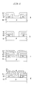
- a p-type diamond substrate 10 is shown schematically.
- a layer 12 of p+ doped amorphous silicon or germanium is applied to the upper surface of the substrate 10 by means of a chemical vapour deposition (CVD) process, or by means of a physical vapour deposition (PVD) process.
- CVD chemical vapour deposition
- PVD physical vapour deposition
- a layer 14 of a first metal is deposited on top of the p+ layer 12, again by means of a CVD or PVD process.
- metals which are suitable are aluminium, molybdenum, molybdenum/tantalum alloy, chrome, titanium, nichrome, titanium/tungsten alloy, palladium, platinum, or an aluminium/silicon alloy.
- a portion of the layers 14 and 12 has been removed selectively by a photolithographic masking and a chemical etching process, exposing the substrate 10 in a region which defines the gate of the transistor. Regions on either side of the gate (G) area define the source (S) and drain (D) of the transistor.
- a layer 16 of a wide-bandgap insulating material is applied over the structure of Figure 1c, again by means of a CVD or PVD process, covering the source, gate and drain regions.
- the insulating material is an oxide, nitride, oxynitride, or a carbide.
- Figure 1e shows a further metallic layer 18, of a second metal which is different from the metal of the layer 14, deposited onto the layer 16 of insulating material.
- a CVD or PVD process is used.
- the second metal although different from the first metal of the layer 14, is selected from the group of metals listed above.
- portions of the layers 18 and 16 are selectively removed by photolithographic masking and chemical etching, to expose the metallic layer 14 above the source and drain regions of the transistor. It can thus be seen that the transistor is provided with metallic contacts of the first metal for the source and drain regions, and a contact of the second metal for the gate region.
- the transistor has a MISFET structure, with the insulating layer 16 lying between the metal gate contact and the p-type semiconductor substrate of the transistor.
- the illustrated transistor has no p-n junctions, a transistor switching action is, nevertheless, obtained. If a positive voltage is applied to the gate contact, a corresponding negative charge is induced in the insulating layer adjacent the gate contact. This is balanced by a positive charge in the insulating layer adjacent the surface of the substrate, which again induces a negative charge in the substrate adjacent its surface. This effectively forms an n-type channel in the substrate between the source and drain regions.
- FIG. 2a to 2d a process for manufacturing a second version of the transistor will be described.
- the second version of the process is similar to that described above, up to the point were the layer 16 of insulating material is applied to the structure illustrated in Figure 1d.
- the structure of Figure 2a therefore corresponds to that of Figure 1d.
- the insulating layer 16 is selectively etched right down to the surface of the substrate 10, to define a gate (G) region.
- a layer 20 of a second metal which differs from the metal of the layer 14, is deposited over the structure by a CVD or PVD process.
- the metallic layer 20 is thus in contact with the surface of the substrate 10 in the gate region.
- the layers 20 and 16 are selectively removed by photolithographic masking and chemical etching, to expose the metal layer 14 above the source and drain regions of the transistor.
- a transistor is thus obtained which has source and drain contacts of the first metal and a gate contact of the second metal.
- the transistor has a MESFET configuration, with the metallic gate contact being directly in contact with the substrate 10 in the gate region of the transistor.
- the layer 16 of insulating material serves to isolate the gate contact from the source and drain contacts.
Landscapes
- Crystals, And After-Treatments Of Crystals (AREA)
- Bipolar Transistors (AREA)
- Junction Field-Effect Transistors (AREA)
- Electrodes Of Semiconductors (AREA)
- Insulated Gate Type Field-Effect Transistor (AREA)
- Weting (AREA)
- Carbon And Carbon Compounds (AREA)
Applications Claiming Priority (2)
| Application Number | Priority Date | Filing Date | Title |
|---|---|---|---|
| GB8812216 | 1988-05-24 | ||
| GB888812216A GB8812216D0 (en) | 1988-05-24 | 1988-05-24 | Diamond transistor method of manufacture thereof |
Publications (3)
| Publication Number | Publication Date |
|---|---|
| EP0343963A2 true EP0343963A2 (de) | 1989-11-29 |
| EP0343963A3 EP0343963A3 (en) | 1990-10-31 |
| EP0343963B1 EP0343963B1 (de) | 1994-09-14 |
Family
ID=10637402
Family Applications (1)
| Application Number | Title | Priority Date | Filing Date |
|---|---|---|---|
| EP89305259A Expired - Lifetime EP0343963B1 (de) | 1988-05-24 | 1989-05-24 | Diamanttransistor und Verfahren zu seiner Herstellung |
Country Status (6)
| Country | Link |
|---|---|
| US (1) | US5072264A (de) |
| EP (1) | EP0343963B1 (de) |
| AT (1) | ATE111637T1 (de) |
| DE (1) | DE68918158T2 (de) |
| GB (1) | GB8812216D0 (de) |
| ZA (1) | ZA893922B (de) |
Cited By (6)
| Publication number | Priority date | Publication date | Assignee | Title |
|---|---|---|---|---|
| EP0450985A3 (en) * | 1990-04-06 | 1991-11-06 | Xerox Corporation | Diamond thin film transistor |
| US5155559A (en) * | 1991-07-25 | 1992-10-13 | North Carolina State University | High temperature refractory silicide rectifying contact |
| US5173761A (en) * | 1991-01-28 | 1992-12-22 | Kobe Steel Usa Inc., Electronic Materials Center | Semiconducting polycrystalline diamond electronic devices employing an insulating diamond layer |
| US5294814A (en) * | 1992-06-09 | 1994-03-15 | Kobe Steel Usa | Vertical diamond field effect transistor |
| US5371378A (en) * | 1992-06-08 | 1994-12-06 | Kobe Steel Usa, Inc. | Diamond metal base/permeable base transistor and method of making same |
| US8193538B2 (en) | 2007-01-22 | 2012-06-05 | Diamond Microwave Devices Limited | Electronic field effect devices |
Families Citing this family (10)
| Publication number | Priority date | Publication date | Assignee | Title |
|---|---|---|---|---|
| AU630663B2 (en) * | 1989-02-01 | 1992-11-05 | Gersan Establishment | P-n-p diamond transistor |
| JPH04302172A (ja) * | 1991-03-29 | 1992-10-26 | Kobe Steel Ltd | ダイヤモンドショットキーダイオード |
| US5254869A (en) * | 1991-06-28 | 1993-10-19 | Linear Technology Corporation | Aluminum alloy/silicon chromium sandwich schottky diode |
| USH1287H (en) | 1992-06-16 | 1994-02-01 | The United States Of America As Represented By The Secretary Of The Navy | Ion implanted diamond metal-insulator-semiconductor field effect transistor |
| JP3117563B2 (ja) * | 1992-11-24 | 2000-12-18 | 株式会社神戸製鋼所 | ダイヤモンド薄膜電界効果トランジスタ |
| US5686737A (en) * | 1994-09-16 | 1997-11-11 | Cree Research, Inc. | Self-aligned field-effect transistor for high frequency applications |
| US5455432A (en) * | 1994-10-11 | 1995-10-03 | Kobe Steel Usa | Diamond semiconductor device with carbide interlayer |
| US6432804B1 (en) * | 2000-05-22 | 2002-08-13 | Sharp Laboratories Of America, Inc. | Sputtered silicon target for fabrication of polysilicon thin film transistors |
| JP2003203930A (ja) * | 2002-01-08 | 2003-07-18 | Nec Compound Semiconductor Devices Ltd | ショットキーゲート電界効果型トランジスタ |
| US7402835B2 (en) * | 2002-07-18 | 2008-07-22 | Chevron U.S.A. Inc. | Heteroatom-containing diamondoid transistors |
Family Cites Families (6)
| Publication number | Priority date | Publication date | Assignee | Title |
|---|---|---|---|---|
| US4016587A (en) * | 1974-12-03 | 1977-04-05 | International Business Machines Corporation | Raised source and drain IGFET device and method |
| JPS58141572A (ja) * | 1982-02-18 | 1983-08-22 | Seiko Epson Corp | 半導体装置 |
| JPS59208821A (ja) * | 1983-05-13 | 1984-11-27 | Sumitomo Electric Ind Ltd | 気相合成によるダイヤモンド半導体およびその製造方法 |
| JPS60246627A (ja) * | 1984-05-21 | 1985-12-06 | Sumitomo Electric Ind Ltd | ダイヤモンド半導体素子 |
| JPS61207078A (ja) * | 1985-03-11 | 1986-09-13 | Sanyo Electric Co Ltd | 電界効果トランジスタ |
| JP2536523B2 (ja) * | 1987-05-14 | 1996-09-18 | 日本電気株式会社 | 半導体装置の製造方法 |
-
1988
- 1988-05-24 GB GB888812216A patent/GB8812216D0/en active Pending
-
1989
- 1989-05-24 US US07/356,776 patent/US5072264A/en not_active Expired - Fee Related
- 1989-05-24 DE DE68918158T patent/DE68918158T2/de not_active Expired - Fee Related
- 1989-05-24 EP EP89305259A patent/EP0343963B1/de not_active Expired - Lifetime
- 1989-05-24 ZA ZA893922A patent/ZA893922B/xx unknown
- 1989-05-24 AT AT89305259T patent/ATE111637T1/de not_active IP Right Cessation
Cited By (11)
| Publication number | Priority date | Publication date | Assignee | Title |
|---|---|---|---|---|
| EP0450985A3 (en) * | 1990-04-06 | 1991-11-06 | Xerox Corporation | Diamond thin film transistor |
| US5173761A (en) * | 1991-01-28 | 1992-12-22 | Kobe Steel Usa Inc., Electronic Materials Center | Semiconducting polycrystalline diamond electronic devices employing an insulating diamond layer |
| US5155559A (en) * | 1991-07-25 | 1992-10-13 | North Carolina State University | High temperature refractory silicide rectifying contact |
| US5371378A (en) * | 1992-06-08 | 1994-12-06 | Kobe Steel Usa, Inc. | Diamond metal base/permeable base transistor and method of making same |
| US5294814A (en) * | 1992-06-09 | 1994-03-15 | Kobe Steel Usa | Vertical diamond field effect transistor |
| US8193538B2 (en) | 2007-01-22 | 2012-06-05 | Diamond Microwave Devices Limited | Electronic field effect devices |
| US8277622B2 (en) | 2007-01-22 | 2012-10-02 | Element Six Ltd. | High uniformity boron doped diamond material |
| US8362492B2 (en) | 2007-01-22 | 2013-01-29 | Diamond Microwave Devices Limited | Electronic field effect devices and methods for their manufacture |
| US8648354B2 (en) | 2007-01-22 | 2014-02-11 | Diamond Microwave Devices Limited | Electronic field effect devices and methods for their manufacture |
| US9034200B2 (en) | 2007-01-22 | 2015-05-19 | Element Six Limited Technologies Limited | Plasma etching of diamond surfaces |
| US10011491B2 (en) | 2007-01-22 | 2018-07-03 | Element Six Technologies Limited | Plasma etching of diamond surfaces |
Also Published As
| Publication number | Publication date |
|---|---|
| GB8812216D0 (en) | 1988-06-29 |
| DE68918158T2 (de) | 1995-01-12 |
| ATE111637T1 (de) | 1994-09-15 |
| DE68918158D1 (de) | 1994-10-20 |
| EP0343963B1 (de) | 1994-09-14 |
| EP0343963A3 (en) | 1990-10-31 |
| US5072264A (en) | 1991-12-10 |
| ZA893922B (en) | 1990-02-28 |
Similar Documents
| Publication | Publication Date | Title |
|---|---|---|
| CA1266812A (en) | Method of fabricating a self-aligned metal- semiconductor fet | |
| EP0343963B1 (de) | Diamanttransistor und Verfahren zu seiner Herstellung | |
| JP3229012B2 (ja) | 半導体装置の製造方法 | |
| EP0224614B1 (de) | Verfahren zum Herstellen eines völlig selbstjustierten Feldeffekttransistors | |
| US4956308A (en) | Method of making self-aligned field-effect transistor | |
| US5739557A (en) | Refractory gate heterostructure field effect transistor | |
| EP0063221B1 (de) | Verfahren zum Herstellen eines Feldeffekttransistors | |
| US4782032A (en) | Method of making self-aligned GaAs devices having TiWNx gate/interconnect | |
| US5182218A (en) | Production methods for compound semiconductor device having lightly doped drain structure | |
| US5550065A (en) | Method of fabricating self-aligned FET structure having a high temperature stable T-shaped Schottky gate contact | |
| US5114871A (en) | Manufacturing diamond electronic devices | |
| US4712291A (en) | Process of fabricating TiW/Si self-aligned gate for GaAs MESFETs | |
| US6617660B2 (en) | Field effect transistor semiconductor and method for manufacturing the same | |
| JPH0312966A (ja) | 電界効果型トランジスタ及び製造方法 | |
| US5236852A (en) | Method for contacting a semiconductor device | |
| US5411903A (en) | Self-aligned complementary HFETS | |
| JPS59181676A (ja) | 半導体装置 | |
| US4727404A (en) | Field effect transistor of the MESFET type for high frequency applications and method of manufacturing such a transistor | |
| US6084258A (en) | Metal-semiconductor junction fet | |
| CA1271850A (en) | Method for fabricating a field-effect transistor with a self-aligned gate | |
| US5254483A (en) | Gate-to-ohmic metal contact scheme for III-V devices | |
| JPH10321843A (ja) | 半導体装置およびその製造方法 | |
| KR950005490B1 (ko) | 인헨스먼트형/디플리션형 전계효과 트랜지스터 및 그 제조방법 | |
| JP3106378B2 (ja) | 半導体装置の製造方法 | |
| JPS6057980A (ja) | 半導体装置の製造方法 |
Legal Events
| Date | Code | Title | Description |
|---|---|---|---|
| PUAI | Public reference made under article 153(3) epc to a published international application that has entered the european phase |
Free format text: ORIGINAL CODE: 0009012 |
|
| AK | Designated contracting states |
Kind code of ref document: A2 Designated state(s): AT BE CH DE ES FR GB GR IT LI LU NL SE |
|
| PUAL | Search report despatched |
Free format text: ORIGINAL CODE: 0009013 |
|
| AK | Designated contracting states |
Kind code of ref document: A3 Designated state(s): AT BE CH DE ES FR GB GR IT LI LU NL SE |
|
| 17P | Request for examination filed |
Effective date: 19901222 |
|
| 17Q | First examination report despatched |
Effective date: 19911211 |
|
| GRAA | (expected) grant |
Free format text: ORIGINAL CODE: 0009210 |
|
| AK | Designated contracting states |
Kind code of ref document: B1 Designated state(s): AT BE CH DE ES FR GB GR IT LI LU NL SE |
|
| PG25 | Lapsed in a contracting state [announced via postgrant information from national office to epo] |
Ref country code: IT Free format text: LAPSE BECAUSE OF FAILURE TO SUBMIT A TRANSLATION OF THE DESCRIPTION OR TO PAY THE FEE WITHIN THE PRE;WARNING: LAPSES OF ITALIAN PATENTS WITH EFFECTIVE DATE BEFORE 2007 MAY HAVE OCCURRED AT ANY TIME BEFORE 2007. THE CORRECT EFFECTIVE DATE MAY BE DIFFERENT FROM THE ONE RECORDED.SCRIBED TIME-LIMIT Effective date: 19940914 Ref country code: GR Free format text: LAPSE BECAUSE OF FAILURE TO SUBMIT A TRANSLATION OF THE DESCRIPTION OR TO PAY THE FEE WITHIN THE PRESCRIBED TIME-LIMIT Effective date: 19940914 Ref country code: AT Effective date: 19940914 Ref country code: ES Free format text: THE PATENT HAS BEEN ANNULLED BY A DECISION OF A NATIONAL AUTHORITY Effective date: 19940914 |
|
| REF | Corresponds to: |
Ref document number: 111637 Country of ref document: AT Date of ref document: 19940915 Kind code of ref document: T |
|
| REF | Corresponds to: |
Ref document number: 68918158 Country of ref document: DE Date of ref document: 19941020 |
|
| ET | Fr: translation filed | ||
| EAL | Se: european patent in force in sweden |
Ref document number: 89305259.7 |
|
| PG25 | Lapsed in a contracting state [announced via postgrant information from national office to epo] |
Ref country code: CH Effective date: 19950531 Ref country code: BE Effective date: 19950531 Ref country code: LI Effective date: 19950531 Ref country code: LU Free format text: LAPSE BECAUSE OF NON-PAYMENT OF DUE FEES Effective date: 19950531 |
|
| PLBE | No opposition filed within time limit |
Free format text: ORIGINAL CODE: 0009261 |
|
| STAA | Information on the status of an ep patent application or granted ep patent |
Free format text: STATUS: NO OPPOSITION FILED WITHIN TIME LIMIT |
|
| 26N | No opposition filed | ||
| BERE | Be: lapsed |
Owner name: DE BEERS INDUSTRIAL DIAMOND DIVISION (PROPRIETARY Effective date: 19950531 |
|
| REG | Reference to a national code |
Ref country code: CH Ref legal event code: PL |
|
| PGFP | Annual fee paid to national office [announced via postgrant information from national office to epo] |
Ref country code: FR Payment date: 19960510 Year of fee payment: 8 |
|
| PGFP | Annual fee paid to national office [announced via postgrant information from national office to epo] |
Ref country code: GB Payment date: 19960515 Year of fee payment: 8 |
|
| PGFP | Annual fee paid to national office [announced via postgrant information from national office to epo] |
Ref country code: SE Payment date: 19960517 Year of fee payment: 8 |
|
| PGFP | Annual fee paid to national office [announced via postgrant information from national office to epo] |
Ref country code: DE Payment date: 19960528 Year of fee payment: 8 |
|
| PGFP | Annual fee paid to national office [announced via postgrant information from national office to epo] |
Ref country code: NL Payment date: 19960529 Year of fee payment: 8 |
|
| PG25 | Lapsed in a contracting state [announced via postgrant information from national office to epo] |
Ref country code: GB Effective date: 19970524 |
|
| PG25 | Lapsed in a contracting state [announced via postgrant information from national office to epo] |
Ref country code: SE Effective date: 19970525 |
|
| PG25 | Lapsed in a contracting state [announced via postgrant information from national office to epo] |
Ref country code: NL Effective date: 19971201 |
|
| GBPC | Gb: european patent ceased through non-payment of renewal fee |
Effective date: 19970524 |
|
| PG25 | Lapsed in a contracting state [announced via postgrant information from national office to epo] |
Ref country code: FR Free format text: LAPSE BECAUSE OF NON-PAYMENT OF DUE FEES Effective date: 19980130 |
|
| EUG | Se: european patent has lapsed |
Ref document number: 89305259.7 |
|
| NLV4 | Nl: lapsed or anulled due to non-payment of the annual fee |
Effective date: 19971201 |
|
| PG25 | Lapsed in a contracting state [announced via postgrant information from national office to epo] |
Ref country code: DE Free format text: LAPSE BECAUSE OF NON-PAYMENT OF DUE FEES Effective date: 19980203 |
|
| REG | Reference to a national code |
Ref country code: FR Ref legal event code: ST |