EP0343664A2 - Verfahren und Vorrichtung zur Prüfung der Seitenwände von Flaschen - Google Patents
Verfahren und Vorrichtung zur Prüfung der Seitenwände von Flaschen Download PDFInfo
- Publication number
- EP0343664A2 EP0343664A2 EP89109450A EP89109450A EP0343664A2 EP 0343664 A2 EP0343664 A2 EP 0343664A2 EP 89109450 A EP89109450 A EP 89109450A EP 89109450 A EP89109450 A EP 89109450A EP 0343664 A2 EP0343664 A2 EP 0343664A2
- Authority
- EP
- European Patent Office
- Prior art keywords
- masking
- area
- defect
- point
- points
- Prior art date
- Legal status (The legal status is an assumption and is not a legal conclusion. Google has not performed a legal analysis and makes no representation as to the accuracy of the status listed.)
- Granted
Links
Images


Classifications
-
- G—PHYSICS
- G01—MEASURING; TESTING
- G01N—INVESTIGATING OR ANALYSING MATERIALS BY DETERMINING THEIR CHEMICAL OR PHYSICAL PROPERTIES
- G01N21/00—Investigating or analysing materials by the use of optical means, i.e. using sub-millimetre waves, infrared, visible or ultraviolet light
- G01N21/84—Systems specially adapted for particular applications
- G01N21/88—Investigating the presence of flaws or contamination
- G01N21/90—Investigating the presence of flaws or contamination in a container or its contents
-
- G—PHYSICS
- G01—MEASURING; TESTING
- G01N—INVESTIGATING OR ANALYSING MATERIALS BY DETERMINING THEIR CHEMICAL OR PHYSICAL PROPERTIES
- G01N21/00—Investigating or analysing materials by the use of optical means, i.e. using sub-millimetre waves, infrared, visible or ultraviolet light
- G01N21/84—Systems specially adapted for particular applications
- G01N21/88—Investigating the presence of flaws or contamination
- G01N21/8806—Specially adapted optical and illumination features
- G01N2021/8829—Shadow projection or structured background, e.g. for deflectometry
- G01N2021/8832—Structured background, e.g. for transparent objects
Definitions
- This invention relates to an apparatus for detecting defects on the sidewalls of bottles.
- the bottles are inspected on parts thereof, i.e., the bodies or sidewalls, bottoms, tops of the mouths. and threaded bottle necks.
- the sidewalls tend to have defects, such as foreign matters or smears which may cause sanitary problems, and cracks, scraches, seeds, blisters, etc. which may cause bottle breakages. It is necessary to inspect the bottles accurately for any these defects.
- the apparatus for detecting defects on bottle sidewalls utilizes the fact that a portion of a defect appears darker than the other portion, in inspecting the sidewalls for defects.
- This apparatus has found it easy to detect defects, such as opaque foreign matters, etc. which are very light blocking, but has found it difficult to detect accurately defects, such as light smears, streaks, blisters, etc. which are opaque and are extended over large areas. That is, a problem with this generally used apparatus is that when the sensitivity of a photoelectric device is increased to detect these opaque large defects, even noises due to different colors, different thicknesses of the sidewalls, etc. are detected as defects.
- a first object of this invention is to provide an apparatus for detecting defect on bottle sidewalls which can detect with high precision opaque defects which are thin and extend over large areas.
- a second object of this invention is to provide an apparatus for detecting defects on bottle sidewalls which can detect opaque defect which are thin and extend over large areas, without changing their contours.
- the first object can be achieved by an apparatus for detecting defects on bottle sidewalls comprising: illumination means for illuminating the sidewall of a bottle; photoelectrically converting means for photoelectrically converting an image of lights transmitted through the sidewall of the bottle illuminated by the illuminating means; defect detecting means for inspecting the transmitted light image photoelectrically converted by the photoelectrically converting means for any defects to detect defects based on brightnesses of at least two points; area-masking means for setting a masking area corresponding to a point to be noted in the transmitted light image, and outputting an area masking signal indicating that the point to be noted is a defect point, based on a distribution of defect points in the masking area; and judging means for judging the presence of a defect on the sidewall of the bottle, based on the area masking signal from the area masking means.
- the second object can be achieved by an apparatus for detecting defects on bottle sidewalls comprising: illumination means for illuminating the sidewall of a bottle; photoelectrically converting means for photoelectrically converting an image of lights transmitted through the sidewall of the bottle illuminated by the illuminating means; defect detecting means for inspecting the transmitted light image photoelectrically converted by the photoelectrically converting means for any defects to detect defects based on brightnesses of at least two points; area-masking means for setting a masking area corresponding to a point to be noted in the transmitted light image, setting in the masking area a plurality of smaller masking areas containing the point to be noted and being smaller than the masking area , finding the point to be noted a defect point when a number of defect points in one of the smaller masking areas is above a set value, and outputting an area masking signal indicating that the point to be noted is a defect point; and judging means for judging the presence of a defect on the sidewall of the bottle, based on the area masking signal from
- Fig. 1 shows the apparatus for detecting defects on bottle sidewalls according to a first embodiment of this invention.
- a bottle 12 to be inspected is continuously conveyed on rotation.
- the bottle 1 is illuminated by a diffusion light source 10 having a surface for emitting even diffused lights.
- a diffusion plate 10a for diffusing the illumination light is disposed on the front of the diffusion light source 10.
- An image of lights transmitted through the sidewall of the bottle 12 is formed in a two-dimensional photoelectric device 16.
- the two-dimensional photoelectric device 16 comprises a light detecting unit, such as an area CCD, for converting the transmitted light image into an electric analog signal, and an optical system for forming the transmitted light image of the bottle 12.
- the optical axis changing unit 14 is disposed in the optical axis of the two-dimensional photoelectric device 16 on the side nearer to the bottle 12 and changes the optical axis of the optical system with respect to the light detecting unit of the two-dimensional photoelectric device 16.
- the optical axis changing unit 14 changes the optical axis in synchronization with a movement of the bottle 12 so that a transmitted light image of the bottle 12 is formed in the light detecting unit of the two-dimensional photoelectic device 16.
- a drive motor 15 swings horizontally a lens 14a disposed on the front of the two-dimensional photoelectric device 16 by a lens driving circuit 21 to change the optical axis.
- An A/D converter 18 converts an analog image signal from the two-dimensional photoelectric device 16 into a digital image signal of a given bits. This digital image signal is supplied to an inspection area/gate setting circuit 20, a monitor display RAM circuit 22 and a defect detection circuit 24.
- the inspection area/gate setting circuit 20 is for setting inspection areas in which the defect detection circuit 24, which will be explained below, detects defects based on the transmitted light image as shown in Fig. 2.
- the inspection area may be determined based on the edges of the transmitted light image of the bottle 12 or may be fixedly determined beforehand. In Fig. 2, the inspection area is set on the entire bottle 12, and the inspection area is divided in five inspection gates 1, 2, 3, 4, 5 in accordance with the profile of the bottle 12.
- the inspection area/gate setting circuit 20 supplies an inspecting gate signal to the monitor display RAM circuit 22, the defect detection circuit 24, a continuous masking circuit 25, an area masking circuit 26 and a judge circuit 28.
- the defect detection circuit 24 Based on the digital image signal from the A/D converter 18, the defect detection circuit 24 compares in brightness a plurality of points spaced from each other vertically and horizontally by a given distance to detect defects. The defect detection circuit 24 outputs a defect detection signal of "1" when a defect is present and outputs a defect detection signal of "0" when a defect is absent.
- the defect detecting system for comparing a plurality of points in brightness includes a two-point defect detection system in which two point are compared in brightness to detect a defect, and a three-point detecting system in which three points are compared in brightness to detect a defect.
- the three-point defect detecting system enables a defect to be detected without failure even when a transmitted light has uneven brightness.
- ⁇ (constant B) when the following formula
- a defect detection signal outputted by the defect detection circuit 24 is subjected to continuous masking by the continuous masking circuit 25.
- the defect detecting circuit 24 increases the sensitivity for the prevention of a defect detection error, sometimes the circuit 24 erroneously detects none defective points as defect points.
- the continuous masking is for removing such erroneous defect points.
- At an actual defect appears continuous defect points having a size corresponding to that of the actual defect. Contrary to this, at a non-defect appears separate defect points.
- the continuous masking circuit 25 outputs a fresh continuous masking signal at each point. For example, when a defect point is actually a defect, a continuous masking signal of "1" is outputted, and when the defect point is not a defect, a continuous masking signal of "0" is outputted.
- a continuous masking signal outputted by the continuous masking circuit 25 is subjected to the area masking by an area masking circuit 26.
- an area masking circuit 26 In the area masking, as shown in Fig. 3, a rectangular masking area Q of 5 rows x 5 columns is set with each point P centered, a number of points in the area Q at which (points) continuous masking signals and defects are added, and, based on whether or not a total number of defect points exceeds a set value, the area masking circuit 26 outputs an area masking signal. That is, an area masking signal is generated only at a portion on which continuous masking signals are concentrated with noises appearing separately being removed.
- Fig. 4 is an example of the area masking circuit 25.
- a continuous masking signal for each image is consecutively inputted to a shift register 50 in synchronization with a clock pulse ⁇ to be shifted and outputted.
- the digit number of the shift register 50 corresponds to a number of rows of the masking area Q.
- continuous masking signals are inputted to the shift register 50 first at the upper left end and then vertically downward.
- the shift register 50 has an adder 51 which adds the values of 5 continuous masking signals. That is, a sum given by the adder 51 gives a sum of the continuous masking signals on each column of the masking region Q.
- RAMs 61, 62, 63, 64, 65 each having a capacity of 500 bits corresponding to the length of the vertical length of the screen.
- a number of the RAMs 61 - 65 corresponds to a number of columns of the masking area Q.
- Addresses to the RAMs 61 - 65 are generated by an address counter 52. Datea are written in the RAMs 61 - 65 through respective write gates 61w - 65w. It is designated by an output of a quinary ring counter 53 which write gate 61w - 65w data is written in.
- the ring counter 53 counts up by one every time the address counter 52 has outputted addresses from 0 to 499.
- a sum given by the adder 51 is written in bits of an address of one of the RAMs 61 - 65 designated by the ring counter 65.
- the address of the RAMs 61 - 65 has been generated by the address counter 52. Accordingly the RAMs 61 - 65 store sums for every five vertically located continuous masking signals for adjacent five columns of the screen.
- Data are read from the RAMs 61 - 65 through read gates 61r - 65r. All the read gates 61r - 65r are kept opened when data are read, so that the data of all the RAMs 61 - 65 including data being currently written are simultaneously read to be outputted to an adder 54.
- the adder 54 adds the data read from the RAMs 61 - 65 and outputs an addition result to a comparator 55. Since the RAMs 61 - 65 correspond to the columns of the masking area Q, the addition result given by the adder 55 is a sum of all the continuous masking signals in the masking area Q.
- the comparator 55 compares this addition result with a set value to output a comparison result as an area masking signal. For example, when the set value is 18, the area masking signal becomes "1" only when the continuous masking signals of 18 or more points in the 5x5 masking area Q are "1", and when less than 18 points have "1", the area masking signal becomes "0".
- the area masking circuit shown in Fig. 4 enables an area masking signal given by area-masking the 5x5 masking area Q to be obtained in real time only by inputting continuous masking signals consecutively in the shift register 50.
- the judge circuit 28 judges the presence of a defect, based on an area masking signal from the area masking circuit 26. For example, the judge circuit 28 counts area masking signals of "1", and when a counted value exceeds a set value, the circuit 28 judges the bottle 12 defective and supplies a judge signal a conveyor system (not shown) of the bottle 12. In response to the judge signal the conveyor system removes the defective bottle.
- a reference signal generator 30 generates a lens swing angle signal and an inspection period signal, based on a bottle position signal from a bottle position detector 32 provided on a rotary table 13 on which the bottle 12 is mounted.
- the lens swing angle signal is for swinging a concave lens 14a so that the transmitted light image of the bottle 12 is formed constantly on the two-dimensional photoelectric device 16 and is supplied to the lens drive circuit 21.
- the lens drive circuit 21 swings the concave lens 14a in accordance with a lens swing angle signal.
- the inspection period signal is indicative of a period in which the concave lens 14a is swinging in accordance with a movement of the bottle 12 and is supplied to the judge circuit 28.
- the lens drive circuit 21 drives the concave lens 14a.
- the lens drive circuit 21 performs feedback control based on a swing angle signal from the concave lens 14a as a feedback signal. When no swing angle signal is supplied by the concave lens 14a, the lens drive circuit 21 performs the control in the open loop.
- An inspection period signal from the reference signal generator 30 is supplied to the judge circuit 30.
- the judge circuit 28 takes as effective only the defect detection signals which are inputted thereto in a period in which the inspection period signal is high level to judge whether or not the bottle 12 is defective. It is also possible to supply an inspection period signal to the inspection area/gate setting circuit 20, the defect detection circuit 24, and the continuous masking circuit 25 or the area masking circuit 26 and take as effective only the inspection period signals which are inputted to the judge circuit 28 in a period in which the inspection period signal is high level.
- the monitor display RAM circuit 22 stores a digital image signal of the bottle 12 in a frame memory built therein to display the image on a monitor 36.
- the monitor display RAM circuit 22 has been supplied with a defect detection signal from the area masking circuit 26, a judge result signal from the judge circuit 28, and an inspection gate signal from the inspection area/gate setting circuit 20. Based on the defect detection signal, a defect point or an error scan are written in the monitor display RAM circuit 22. Based on the inspection gate signal, a corresponding inspection gate is displayed on the monitor 36.
- the continuous masking is followed by the area masking. This enables a defect to be detected without any errors even when noises are generated due to an increase in the sensitivity. That is, this is because the continuous masking signals indicative of noises are isolated as shown in Fig. 6(a), while the continuous masking signals indicative of opaque defects, such as light smears, streaks, blisters, etc., are scattered as shown in Fig. 6(b), which enables noises and opaque defects to be discriminated from each other.
- Fig. 7 shows the apparatus for detecting defects on bottle sidewalls according to a second embodiment of this invention.
- the members common with the first embodiment have share the same reference numerals not to repeat their explanations.
- the second embodiment is characterized by a masking unit 27 for masking a defect detection signal from a defect detection circuit 24.
- the masking unit 27 of this embodiment is shown in Fig. 8 in good detail.
- the masking unit 27 comprises a continuous masking circuit 25 and an area masking circuit 26.
- a defect detection signal from the defect detection circuit 24 is masked first by the continuous masking circuit 25, and then an output signal from the continuous masking circuit 25 is masked by the area masking circuit 26.
- the continuous masking circuit 24 of this embodiment is the same as that of the first embodiment and omits as actually non-defects the defect points which are isolated or are continuous only below a set value to ouput a fresh continuous masking signal for each point.
- a continuous masking signal from the continuous masking circuit 25 is area-masked by the area masking circuit 26, and an area masking signal is outputted.
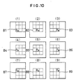
- a rectangular masking area Q of 5 rows x 5 columns for example, is set with a point to be noted (P33) centered as shown in Fig. 9.
- P33 point to be noted
- a rectangular masking area Q of 5 rows x 5 columns for example, is set with a point to be noted (P33) centered as shown in Fig. 9.
- P33 point to be noted
- the masking area Q are set smaller masking areas q1 - q9 of, e.g., 3 rows x 3 columns with the point to be noted P33 contained.
- the numbers of defect points in the smaller masking areas q1 - q9 are added, and when the total number of defect points in one of the smaller masking areas exceed a set value NR, and further the point to be noted P (P33) is a defect point, the point to be noted P (P33) is found a defect point.
- Such area masking generates an area masking signal only at a portion where defect points indicated by continuous masking signals are concentrated, while noises, which are indicated by isolated defect points, are removed. Accordingly the contour of a defect which has been area-masked is not much changed.
- FIG. 11 An example of the area masking circuit 26 is shown in Fig. 11.
- Continuous masking signals for respective images are inputted consecutively to a flip-flop 70 in synchronization with a clock signal ⁇ and outputted.
- continuous masking signals are consecutively inputted in the flip-flop 70 first at the upper left end and vertically downward.
- RAMS 81, 82, 83, 84, 85 each having a capacity of 500 bits corresponding to the length of the vertical length of the screen.
- a number of the RAMs 81 - 85 corresponds to a number of columns of the masking area Q.
- Addresses to the RAMs 81 - 85 are generated by an address counter 72.
- Data are written in the RAMs 81 - 85 through respective write gates 81w - 85w. It is designed by an output of a quinary ring counter 73 which write gate 81w - 85w data is written in.
- the ring counter 73 counts up by one every time the address counter 72 has outputted addresses from 0 to 499.
- the continuous masking signals retained by the flip-flop 70 are written in the one of the RAMs 81 - 85 designated by a ring counter 73 at bits of an address generated by an address counter 72. Accordingly, the RAMs 81 - 85 store continuous masking signals for adjacent 5 columns of the screen.
- Continuous masking signals are read from the RAMs 81 - 85 through read gates 81r - 85r.
- a continuous masking signal being currently written is read directly at a read gate 81r - 85r associated with the one of the read gates 81r - 85r designated by an output of a ring counter 73.
- continuous masking signal are read from the associated RAMs 81 - 85.
- the ring counter 73 designates the read gate 81w, and a continuous masking signal is being written in the RAM 81, the continuous masking signal currently being written is read directly at the read gate 81r, while the continuous masking signals stored in the RAMs 82r - 85r are read through read gates 82r - 85r.
- the continuous masking signals read through the read gates 81r - 85r are re-arranged in order by a re-arranging circuit 90 to be stored in respective 5-digit shift registers 91 - 95.
- a number of digits of the shift registers 91 - 95 corresponds to a number of columns of the masking area Q.
- the re-arranging circuit 90 puts into another order the continuous masking signals read through the read gates 81r - 85r, based on an output from the ring counter 73 so that the outputs from the respective shift registers 91 - 95 are placed in a preset order of continuous masking signals as shown in Fig. 11.
- adders 101 - 109 corresponding to the smaller masking areas q1 - q9 of Fig. 10, and the adders 101 - 109 add continuous masking siganls P11 - P55 for the points defining the respective smaller masking sreas q1 - q9 which are supplied by the shift registers 91 - 95.
- the adder 101 adds the continuous masking signals P11, P12, P13, P21, P22, P23, P31, P32 and P33 which define the smaller masking area q1 of Fig. 10(1).
- Addition results of the adders 101 - 109 are compared with a set value NR by comparators 111 - 119.
- a nine-input OR gate 120 gives a logical sum of comparison results of the comparators 111 - 119, and an AND gate gives a logical product of an output of the OR gate 120 with the continuous masking signal P33 of the point to be noted P.
- An output signal from the AND gate 121 is an area masking signal.
- the area masking circuit of Fig. 11 enables an area masking signal which has been given by area-masking a 5x5 masking area Q to be obtained in real time only by inputting consecutively continuous masking signals to the flip-flop 70.
- a judge circuit 28 judges the presence of a defect, based on an area masking signal supplied by the area masking circuit 26.
- Fig. 12 shows a first modification of the masking unit 27.
- a defect detection signal from the defect detection circuit 24 is supplied to the continuous masking unit 25 and the area masking circuit 26 so that the continuous masking the area-masking are performed parallelly.
- the continuous masking circuit 25 performs continuous masking on a defect detection signal to output a continuous masking signal
- the area masking circuit 26 performs the area-masking on the defect detection signal to output an area masking signal.
- An AND gate 29 gives a logical product of the continuous masking signal and an area masking signal of each point to supply an output signal to the judge circuit 28.
- Fig. 13 shows a second modification of the masking unit 27.
- the masking unit 27 is provided by only an area masking circuit 27.
- the area masking circuit 27 area-masks a defect detection signal from the defect detection circuit 21 to output an area masking signal to the judge circuit 28.
- the masking area Q for the area masking is 5 columns x 5 rows, and the smaller masking area q is 3 columns x 3 rows.
- These areas may be larger, e.g., the former may be 9 columns x 9 rows, and the latter being 5 columns x 5 rows.
- the masking area Q and the smaller masking area q may be horizontally elongate or vertically elongate.
- a horizontally elongate masking area Q exemplified in Fig. 14 prevents the erroneous detection of a joint R running vertically on the bottle 12 which was formed in manufacturing the bottle 12. That is, in the case where the direction of a matter, such as a joint R, which preferably is not detected as a defect is known beforehand, the masking area Q is set horizontal to the direction of the matter.
- the bottle continuously conveyed is followed by changing the optical axis of the two-dimensional photoelectric device 16, but instead a mirror is used to follow the bottle 12.
- the two dimensional photoelectric device 16 is used to detect a transmitted light image of the bottle 12, but instead a one dimensional photoelectric device, such as linear CCD, may be used.
- This invention is usable in detecting defects on the surface of, e.g., metal parts, plastics etc. other than bottles.
Landscapes
- Physics & Mathematics (AREA)
- Health & Medical Sciences (AREA)
- Life Sciences & Earth Sciences (AREA)
- Chemical & Material Sciences (AREA)
- Analytical Chemistry (AREA)
- Biochemistry (AREA)
- General Health & Medical Sciences (AREA)
- General Physics & Mathematics (AREA)
- Immunology (AREA)
- Pathology (AREA)
- Investigating Materials By The Use Of Optical Means Adapted For Particular Applications (AREA)
Applications Claiming Priority (2)
| Application Number | Priority Date | Filing Date | Title |
|---|---|---|---|
| JP63128247A JPH0641924B2 (ja) | 1988-05-27 | 1988-05-27 | 壜胴部の欠陥検出装置 |
| JP128247/88 | 1988-05-27 |
Publications (3)
| Publication Number | Publication Date |
|---|---|
| EP0343664A2 true EP0343664A2 (de) | 1989-11-29 |
| EP0343664A3 EP0343664A3 (en) | 1990-08-29 |
| EP0343664B1 EP0343664B1 (de) | 1996-05-01 |
Family
ID=14980133
Family Applications (1)
| Application Number | Title | Priority Date | Filing Date |
|---|---|---|---|
| EP89109450A Expired - Lifetime EP0343664B1 (de) | 1988-05-27 | 1989-05-25 | Verfahren und Vorrichtung zur Prüfung der Seitenwände von Flaschen |
Country Status (4)
| Country | Link |
|---|---|
| US (1) | US4948956A (de) |
| EP (1) | EP0343664B1 (de) |
| JP (1) | JPH0641924B2 (de) |
| DE (1) | DE68926362T2 (de) |
Cited By (6)
| Publication number | Priority date | Publication date | Assignee | Title |
|---|---|---|---|---|
| DE4130373A1 (de) * | 1990-09-19 | 1992-03-26 | Hajime Industries | Pruefverfahren und pruefvorrichtung |
| GB2252624A (en) * | 1991-01-24 | 1992-08-12 | Hajime Industries | Defect detection by image analysis using two neighbouring inspection zones |
| EP0610956A3 (de) * | 1993-02-12 | 1994-11-02 | Fuji Electric Co Ltd | Prüfvorrichtung für die innere Oberfläche eines Behälters. |
| EP1598662A1 (de) * | 2004-05-17 | 2005-11-23 | Total Petrochemicals Research Feluy | Verfahren zur Quantifizierung der optischen Eigenschaften von Kunststoff Formteile |
| US7060999B2 (en) | 2004-07-09 | 2006-06-13 | Owens-Brockway Glass Container Inc. | Apparatus and method for inspecting ribbed containers |
| EP1988388A2 (de) | 2007-05-02 | 2008-11-05 | Emhart Glass S.A. | Maschine zur Überprüfung von Glasbehältern |
Families Citing this family (18)
| Publication number | Priority date | Publication date | Assignee | Title |
|---|---|---|---|---|
| CA2058242C (en) * | 1990-12-20 | 1996-12-17 | Yutaka Hashimoto | Print monitoring apparatus |
| US5412203A (en) * | 1991-07-15 | 1995-05-02 | Fuji Electric Co., Ltd. | Cylindrical container inner surface tester |
| JP2756386B2 (ja) * | 1991-12-27 | 1998-05-25 | 日本たばこ産業株式会社 | 円筒形物体の外観検査装置 |
| ATE139468T1 (de) * | 1992-11-27 | 1996-07-15 | Elpatronic Ag | Verfahren zum ausscheiden von mehrwegflaschen aus dem mehrwegumlauf |
| US5466927A (en) * | 1994-04-08 | 1995-11-14 | Owens-Brockway Glass Container Inc. | Inspection of translucent containers |
| US5486692A (en) * | 1994-10-19 | 1996-01-23 | Emhart Glass Machinery Investments Inc. | Glassware inspection machine comprising diffused light sources and two-dimensional cameras |
| CH688663A5 (de) * | 1994-10-20 | 1997-12-31 | Elpatronic Ag | Verfahren und Vorrichtung zur Inspektion von Gegenstaenden, insbesondere von Flaschen. |
| AU6640396A (en) * | 1995-07-31 | 1997-02-26 | Coors Brewing Company | Hot bottle inspection apparatus and method |
| US6025910A (en) * | 1995-09-12 | 2000-02-15 | Coors Brewing Company | Object inspection method utilizing a corrected image to find unknown characteristic |
| US6025919A (en) * | 1996-08-16 | 2000-02-15 | Coors Brewing Company | Method for measurement of light transmittance |
| US6118526A (en) * | 1996-08-16 | 2000-09-12 | Coors Brewing Company | Method for measurement of light transmittance |
| US5935285A (en) * | 1997-12-30 | 1999-08-10 | Coors Brewing Company | Method for inspecting manufactured articles |
| US6049379A (en) * | 1997-12-30 | 2000-04-11 | Coors Brewing Company | Method for inspecting translucent objects using imaging techniques |
| US6473169B1 (en) | 2000-05-03 | 2002-10-29 | Air Logic Power Systems, Inc. | Integrated leak and vision inspection system |
| US7342654B2 (en) * | 2003-12-19 | 2008-03-11 | International Business Machines Corporation | Detection of impurities in cylindrically shaped transparent media |
| US7595870B2 (en) * | 2004-11-10 | 2009-09-29 | Owens-Brockway Glass Container Inc. | Optical inspection of container walls |
| DE102009020919A1 (de) | 2009-05-12 | 2010-11-18 | Krones Ag | Vorrichtung zum Erkennen von Erhebungen und/oder Vertiefungen auf Flaschen, insbesondere in einer Etikettiermaschine |
| DE102009020920A1 (de) * | 2009-05-12 | 2010-11-18 | Krones Ag | Inspektionsvorrichtung zur Erkennung von Embossings und/oder Etiketten auf transparenten Gefäßen, insbesondere Getränkeflaschen |
Family Cites Families (12)
| Publication number | Priority date | Publication date | Assignee | Title |
|---|---|---|---|---|
| JPS4934385A (de) * | 1972-07-28 | 1974-03-29 | ||
| JPS5546172A (en) * | 1978-09-29 | 1980-03-31 | Kirin Brewery Co Ltd | Detector for foreign material |
| US4300122A (en) * | 1979-04-02 | 1981-11-10 | Sperry Corporation | Apparatus for processing digital data representative of a two-dimensional image |
| US4492476A (en) * | 1981-02-20 | 1985-01-08 | Kirin Beer Kabushiki Kaisha | Defect detecting method and apparatus |
| JPS57178486A (en) * | 1981-04-25 | 1982-11-02 | Nippon Kogaku Kk <Nikon> | Smoothing device for binary image signal |
| JPS5821146A (ja) * | 1981-07-30 | 1983-02-07 | Kirin Brewery Co Ltd | 欠陥検査方法および装置 |
| US4549205A (en) * | 1982-05-10 | 1985-10-22 | Takeda Chemical Industries, Ltd. | Ampoule inspecting method |
| JPH0612344B2 (ja) * | 1982-08-31 | 1994-02-16 | サントリー株式会社 | 瓶類のスカッフ程度検査装置 |
| IL79098A0 (en) * | 1985-07-15 | 1986-09-30 | Visionetics Corp | Fine flaw detector for printed circuit boards |
| US4742399A (en) * | 1985-11-01 | 1988-05-03 | Dainippon Screen Mfg. Co., Ltd. | Method of and apparatus for generating high-resolution bilevel image data |
| JPS6396095A (ja) * | 1986-10-13 | 1988-04-26 | 株式会社キリンテクノシステム | 壜のねじ口部検査装置 |
| JPS63304146A (ja) * | 1987-06-04 | 1988-12-12 | Kirin Brewery Co Ltd | 壜の胴部検査装置 |
-
1988
- 1988-05-27 JP JP63128247A patent/JPH0641924B2/ja not_active Expired - Lifetime
-
1989
- 1989-05-25 DE DE68926362T patent/DE68926362T2/de not_active Expired - Fee Related
- 1989-05-25 EP EP89109450A patent/EP0343664B1/de not_active Expired - Lifetime
- 1989-05-26 US US07/357,288 patent/US4948956A/en not_active Expired - Lifetime
Cited By (8)
| Publication number | Priority date | Publication date | Assignee | Title |
|---|---|---|---|---|
| DE4130373A1 (de) * | 1990-09-19 | 1992-03-26 | Hajime Industries | Pruefverfahren und pruefvorrichtung |
| GB2252624A (en) * | 1991-01-24 | 1992-08-12 | Hajime Industries | Defect detection by image analysis using two neighbouring inspection zones |
| EP0610956A3 (de) * | 1993-02-12 | 1994-11-02 | Fuji Electric Co Ltd | Prüfvorrichtung für die innere Oberfläche eines Behälters. |
| EP1598662A1 (de) * | 2004-05-17 | 2005-11-23 | Total Petrochemicals Research Feluy | Verfahren zur Quantifizierung der optischen Eigenschaften von Kunststoff Formteile |
| WO2005111589A3 (en) * | 2004-05-17 | 2007-05-18 | Total Petrochemicals Res Feluy | A method for quantifying the optical properties of moulded objects |
| US7060999B2 (en) | 2004-07-09 | 2006-06-13 | Owens-Brockway Glass Container Inc. | Apparatus and method for inspecting ribbed containers |
| EP1988388A2 (de) | 2007-05-02 | 2008-11-05 | Emhart Glass S.A. | Maschine zur Überprüfung von Glasbehältern |
| EP1988388A3 (de) * | 2007-05-02 | 2010-07-28 | Emhart Glass S.A. | Maschine zur Überprüfung von Glasbehältern |
Also Published As
| Publication number | Publication date |
|---|---|
| EP0343664B1 (de) | 1996-05-01 |
| JPH0641924B2 (ja) | 1994-06-01 |
| JPH01299444A (ja) | 1989-12-04 |
| EP0343664A3 (en) | 1990-08-29 |
| US4948956A (en) | 1990-08-14 |
| DE68926362T2 (de) | 1996-12-12 |
| DE68926362D1 (de) | 1996-06-05 |
Similar Documents
| Publication | Publication Date | Title |
|---|---|---|
| US4948956A (en) | Apparatus with area-masking for detecting defects on bottle sidewalls | |
| US4679075A (en) | Glassware inspection using optical streak detection | |
| EP0597639B1 (de) | Berührungslose Erkennung von Oberflächenfehlern | |
| US4579455A (en) | Photomask inspection apparatus and method with improved defect detection | |
| CA2053176C (en) | Method of and apparatus for inspecting bottle or the like | |
| EP0344617B1 (de) | Verfahren und Vorrichtung zur Prüfung der Seitenwände von Flaschen | |
| CA1175139A (en) | Defect detecting method and device | |
| EP0337421B1 (de) | Verfahren und Vorrichtung zur Prüfung der Seitenwand einer Flasche | |
| US4492476A (en) | Defect detecting method and apparatus | |
| JP3497297B2 (ja) | 容器底部の環状ナール領域検査装置 | |
| US5481619A (en) | Inspection method using templates images, unique histogram analysis, and multiple gray levels correlated to addresses of template images | |
| JPH04220551A (ja) | 透明物体の欠陥検査方法とその装置 | |
| JPH01199139A (ja) | 対象物の透明度のコントラストにより対象物を検査する方法に用いる回路 | |
| EP0293510B1 (de) | Vorrichtung zur Prüfung der Seitenwand einer Flasche | |
| US4549205A (en) | Ampoule inspecting method | |
| JPH05264467A (ja) | 繰返しパターンの欠陥検査装置 | |
| US4983822A (en) | Variable optical axis type bottle inspecting apparatus | |
| JP3055323B2 (ja) | 円形容器内面検査装置 | |
| JP3391163B2 (ja) | 円形容器内面検査装置 | |
| JPH06103277B2 (ja) | 壜胴部の欠陥検出装置 | |
| JPH0694645A (ja) | 円形容器内面検査装置 | |
| Wilder et al. | Automatic plaque assay for the pharmaceutical industry using machine vision | |
| JPH05264464A (ja) | 繰返しパターンの欠陥検査装置 | |
| MXPA99004896A (en) | Inspection of containers through the use of a single area arrangement detector and selected light sources alternativame |
Legal Events
| Date | Code | Title | Description |
|---|---|---|---|
| PUAI | Public reference made under article 153(3) epc to a published international application that has entered the european phase |
Free format text: ORIGINAL CODE: 0009012 |
|
| AK | Designated contracting states |
Kind code of ref document: A2 Designated state(s): DE FR GB |
|
| PUAL | Search report despatched |
Free format text: ORIGINAL CODE: 0009013 |
|
| AK | Designated contracting states |
Kind code of ref document: A3 Designated state(s): DE FR GB |
|
| RAP1 | Party data changed (applicant data changed or rights of an application transferred) |
Owner name: KABUSHIKI KAISHA KIRIN TECHNO SYSTEM |
|
| 17P | Request for examination filed |
Effective date: 19910221 |
|
| 17Q | First examination report despatched |
Effective date: 19920918 |
|
| GRAH | Despatch of communication of intention to grant a patent |
Free format text: ORIGINAL CODE: EPIDOS IGRA |
|
| GRAA | (expected) grant |
Free format text: ORIGINAL CODE: 0009210 |
|
| AK | Designated contracting states |
Kind code of ref document: B1 Designated state(s): DE FR GB |
|
| REF | Corresponds to: |
Ref document number: 68926362 Country of ref document: DE Date of ref document: 19960605 |
|
| ET | Fr: translation filed | ||
| PLBE | No opposition filed within time limit |
Free format text: ORIGINAL CODE: 0009261 |
|
| STAA | Information on the status of an ep patent application or granted ep patent |
Free format text: STATUS: NO OPPOSITION FILED WITHIN TIME LIMIT |
|
| 26N | No opposition filed | ||
| REG | Reference to a national code |
Ref country code: GB Ref legal event code: IF02 |
|
| PGFP | Annual fee paid to national office [announced via postgrant information from national office to epo] |
Ref country code: GB Payment date: 20040617 Year of fee payment: 16 |
|
| PGFP | Annual fee paid to national office [announced via postgrant information from national office to epo] |
Ref country code: FR Payment date: 20040618 Year of fee payment: 16 |
|
| PGFP | Annual fee paid to national office [announced via postgrant information from national office to epo] |
Ref country code: DE Payment date: 20040726 Year of fee payment: 16 |
|
| PG25 | Lapsed in a contracting state [announced via postgrant information from national office to epo] |
Ref country code: GB Free format text: LAPSE BECAUSE OF NON-PAYMENT OF DUE FEES Effective date: 20050525 |
|
| PG25 | Lapsed in a contracting state [announced via postgrant information from national office to epo] |
Ref country code: DE Free format text: LAPSE BECAUSE OF NON-PAYMENT OF DUE FEES Effective date: 20051201 |
|
| GBPC | Gb: european patent ceased through non-payment of renewal fee |
Effective date: 20050525 |
|
| PG25 | Lapsed in a contracting state [announced via postgrant information from national office to epo] |
Ref country code: FR Free format text: LAPSE BECAUSE OF NON-PAYMENT OF DUE FEES Effective date: 20060131 |
|
| REG | Reference to a national code |
Ref country code: FR Ref legal event code: ST Effective date: 20060131 |