EP0343633A2 - Circuit intégré semi-conducteur - Google Patents
Circuit intégré semi-conducteur Download PDFInfo
- Publication number
- EP0343633A2 EP0343633A2 EP89109390A EP89109390A EP0343633A2 EP 0343633 A2 EP0343633 A2 EP 0343633A2 EP 89109390 A EP89109390 A EP 89109390A EP 89109390 A EP89109390 A EP 89109390A EP 0343633 A2 EP0343633 A2 EP 0343633A2
- Authority
- EP
- European Patent Office
- Prior art keywords
- lead
- integrated circuit
- semiconductor integrated
- circuit according
- inner lead
- Prior art date
- Legal status (The legal status is an assumption and is not a legal conclusion. Google has not performed a legal analysis and makes no representation as to the accuracy of the status listed.)
- Ceased
Links
Images


Classifications
-
- H—ELECTRICITY
- H10—SEMICONDUCTOR DEVICES; ELECTRIC SOLID-STATE DEVICES NOT OTHERWISE PROVIDED FOR
- H10W—GENERIC PACKAGES, INTERCONNECTIONS, CONNECTORS OR OTHER CONSTRUCTIONAL DETAILS OF DEVICES COVERED BY CLASS H10
- H10W70/00—Package substrates; Interposers; Redistribution layers [RDL]
- H10W70/40—Leadframes
- H10W70/421—Shapes or dispositions
-
- H—ELECTRICITY
- H10—SEMICONDUCTOR DEVICES; ELECTRIC SOLID-STATE DEVICES NOT OTHERWISE PROVIDED FOR
- H10W—GENERIC PACKAGES, INTERCONNECTIONS, CONNECTORS OR OTHER CONSTRUCTIONAL DETAILS OF DEVICES COVERED BY CLASS H10
- H10W72/00—Interconnections or connectors in packages
- H10W72/50—Bond wires
- H10W72/541—Dispositions of bond wires
- H10W72/547—Dispositions of multiple bond wires
- H10W72/5473—Dispositions of multiple bond wires multiple bond wires connected to a common bond pad
-
- H—ELECTRICITY
- H10—SEMICONDUCTOR DEVICES; ELECTRIC SOLID-STATE DEVICES NOT OTHERWISE PROVIDED FOR
- H10W—GENERIC PACKAGES, INTERCONNECTIONS, CONNECTORS OR OTHER CONSTRUCTIONAL DETAILS OF DEVICES COVERED BY CLASS H10
- H10W90/00—Package configurations
- H10W90/701—Package configurations characterised by the relative positions of pads or connectors relative to package parts
- H10W90/751—Package configurations characterised by the relative positions of pads or connectors relative to package parts of bond wires
- H10W90/756—Package configurations characterised by the relative positions of pads or connectors relative to package parts of bond wires between a chip and a stacked lead frame, conducting package substrate or heat sink
Definitions
- the present invention relates to a semiconductor integrated circuit with lessened adverse effects by a power noise due to an overcurrent.
- An integrated circuit with a single or a plurality of functions in which a great number of semiconductor elements are integrated into a single chip, is well known as a called IC.
- the IC chip is housed in a cavity for protecting it from deteriorating and deleterious effects by the surrounding atmosphere.
- the semiconductor chip contains many pad electrodes for signal transfers and power supplies.
- Fig. 1 illustrates a block diagram of a typical circuit contained in a memory IC chip.
- Address signals applied from exterior to the memory circuit first reach pad electrodes 11, ..., 11 of the memory circuit. The address signals are then inputted to an address buffer circuit 12 and to an address decoder circuit 13.
- decode signals outputted from the address decoder circuit 13 data of a plurality of bits are read out of a memory 14, and amplified by a sense amplifier circuit 15.
- the amplified data signals are applied to an output circuit 16 and subsequently to an output buffer circuit 17.
- the data signals loaded in the output buffer circuit 17 is outputted outside through pad electrodes 18, ..., 18.
- a power voltage Vcc is applied to a power pad electrode 19.
- Two ground voltages Vss1 and Vss2 are respectively applied to pads 20 and 21 exclusively used for ground voltage application.
- Pad electrodes 18, ..., 18 for data outputting contain parasitic capacitances that are treated as a load capacitor 24.
- the power voltage Vcc applied to the pad electrode 19 is supplied to an internal circuit 22 and a peripheral circuit 23.
- the internal circuit 22 is made up of the address buffer 12, address decoder 13, memory 14 and sense amplifier circuit 15.
- the peripheral circuit 23 is made up of the output circuit 16 and the output buffer circuit 17.
- the ground voltage Vss1 is applied to the internal circuit 22.
- the ground voltage Vss2 is applied to the peripheral circuit 23. The reason why two different ground voltages are applied to those circuits will be described below.
- Static RAMs and ROMs as typical memory ICs generally use multi-bit of 8 bits or 16 bits, for example, for the output data.
- the load capacitor 24 parasitic on the pad electrodes for outputting the multibit data is usually about 100 pF.
- it is required to simultaneously charge and discharge of a plurality of load capacitors. At this time, large currents caused by the charge discharge flow through the power interconnections in the chip. Particularly for the ground voltage interconnections that is long in length and high in line resistance and inductance, the flowing of large current therethrough results in a great variation of the ground voltages.
- the ground voltage Vss1 is applied to the internal circuit 22, and another ground voltage Vss2 to the peripheral circuit 23 containing the output buffer through which a large current possibly flows. With such ground voltage supplies, even when noise is generated in the ground voltage Vss2, the ground voltage Vss1 is isolated from that noise. In other memory circuits, the ground potential Vss1 is applied to the output circuit 16 as well as the internal circuit 22, and the ground voltage Vss2 is applied to only the output buffer 17.
- the IC package is provided with a lead frame containing inner leads and outer lead integral with the inner leads, in addition to the semiconductor chip.
- the tips or ends of the inner leads are electrically coupled with the pad electrodes by means of metal wires of Au or Al, for example, that are called bonding wires.
- the inner leads, together with the semiconductor chip are hermetically encapsulated into a cavity, while the outer leads being left outside the cavity. Then, the outer leads are bent and cut as required, and are used as the external terminals of the DIP type.
- Fig. 2 shows the innards of a conventional IC package with 28 pins that houses a memory IC chip.
- a memory IC chip 31 is provided with many pad electrodes including a pad electrode 19 for the power voltage Vcc, and pad electrodes 20 and 21 for the ground voltages Vss1 and Vss2.
- Reference number 32, ..., 32 designate inner leads on a lead frame; 33 bonding wires; and 34 a cavity. In the illustration, other pad electrodes than those for power voltages and the outer leads on the lead frame are omitted for simplicity.
- the ground voltage for use in the circuits handling large currents such as the output buffer is different from the ground voltage for the remaining circuits.
- the lead frame is common for both the inner and output leads.
- L 2l (ln + 0.5 + 0.224 ) (nH) (1)
- l Length of the inner lead
- w Width of the same
- t Thickness of the same.
- FIG. 3 A portion including mainly the output buffer circuit 17 may equivalently be depicted as shown in Fig. 3.
- C represents the load capacitance
- Q an n-channel output transistor in the output buffer circuit 17 which is for discharging the load capacitor C
- L an self-inductance component existing in the inner lead on the lead frame for the ground voltage supply.
- the equivalent circuit of Fig. 3 represents the memory device when the discharge of the load capacitor C progresses.
- a p-channel output transistor for charging purposes which is connected to a power voltage Vcc in the output buffer is in an off state. Therefore, it is omitted in the illustration.
- the equivalent channel width W and channel length L of the output transistor Q for 8 bits are 2400 ⁇ m and 2.2 ⁇ m.
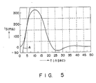
- a variation of a discharge current Is was simulated by a computer under conditions that the load capacitor C is charged at 5V by a signal Din and a signal Din as shown in Fig. 4 is applied to the gate of the output transistor Q.
- the variation of the discharge current Is simulated was as shown in Fig. 5.
- Noise appearing in the ground voltage Vss2 is proportional to a rate of change of the discharge current Is with respect to time "t", viz., dIs/dt.
- a maximum changing rate of discharge current, i.e., dIs/dt (max) is defined by an inclination of a slanted line A, and approximately 78 x 106 (A/sec).
- Vss2(max) L x dIs/dt(max) (2)
- a potential at the pad electrode 21 which should be at 0V rises up to a maximum of 1V. This great voltage variation at the electrode 21 transfers to the pad electrode 20. Because of this, the internal circuit of the conventional memory IC tends to improperly operate.
- an object of the present invention is to provide a semiconductor integrated circuit which minimizes the power noise in the power supply path, thereby almost eliminating the improper operation of the internal circuit.
- a semiconductor integrated circuit comprising: a semiconductor chip having a plurality of pad electrodes on a major surface thereof; a cavity for housing the semiconductor chip; a plurality of lead frames each being made up of an inner lead and an outer lead; metal wires each for electrically connecting the tip of each the inner lead to one pad electrode; and one of the plurality of lead frames whose inner lead has a larger area than those of the other lead frames, the lead frame supplying a power voltage.
- a semiconductor integrated circuit comprising: a semiconductor chip having a plurality of pad electrodes on a major surface thereof; a cavity for housing the semiconductor chip; a plurality of lead frames each being made up of an inner lead and an outer lead, metal wires each for electrically connecting the tip of each the inner lead to one pad electrode; and one of the plurality of lead frames whose inner lead is branched into a plurality of leads, the lead frame supplying a power voltage.
- FIG. 6 there is shown in a package of a semiconductor integrated circuit according to a first embodiment of the present invention.
- the integrated circuit (IC) package like the IC package already described with reference to Fig. 2, uses a memory IC chip 31 with two pad electrodes 20 and 21 for receiving two ground voltages Vss1 and Vss2.
- reference numerals 32 designate inner leads as lead frames; 33 bonding wires; and 34 a cavity.
- the pad electrode for the other power voltage than the ground voltages is omitted as well as the outer leads as the lead frames.
- Fig. 7 perspectively showing an appearance of the IC package under discussion, outer leads 35 as lead frames are led out outside the cavity, are properly bent and cut, and are used as external terminals of the dual-in-line (DIP) type.
- DIP dual-in-line
- the inner leads 32 for the supply of the ground voltages Vss1 and Vss2 are each branched into two leads 32A and 32B at the portion where is closer to the corner of the cavity 34 and the outer lead 35 (not shown in Fig. 6, but shown in Fig. 7) terminates.
- Bonding wires 33 electrically connects the tips of the inner leads 32A and 32B to the two pad electrodes 20 and 21 on the chip surface, respectively.
- the ground voltage Vss2 is stable irrespective of the current variation in the output buffer.
- the proper operation of the internal circuit 22 is always ensured.
- the connections using the branched inner leads is advantageous particularly in the recent high speed memory devices, because these require the flow of simultaneous large current into the output buffer.
- the internal circuit is insensitive to the power noise.
- FIG. 8 there is shown a second embodiment of a semiconductor integrated circuit according to the present invention.
- the figure shows a pattern inside a cavity 34 which contains lead frames and a bed 36 on which a semiconductor chip is placed.
- pins 37 and 38 are continuous to the bed 36, and for suspending the bed.
- Supports 39 which are continuous to the suspending pins 37 and 38, fixedly supports these pins.
- an inner lead 32 exclusively used for the ground voltage supply forks two parts in the vicinity of a corner of the cavity 34; one part constitutes an inner lead 32A for the ground voltage Vss1 and the other another inner lead 32B for the ground voltage Vss2.
- An inner lead 32C for the power voltage Vcc has a larger area than each inner lead (not shown) for signal input/output use.
- pins 40 are provided at the four corners of the cavity 34. These pins 40 fix the inner leads including the inner leads for the power supply that are laid out at the four corners of the cavity, against their displacement from the correct positions, which possibly occurs when the cavity 34 is formed by a resin molding process, e.g., a transfer molding process.
- the feature of a large area of the inner lead 32C for the Vcc voltage effectively reduces the power noise generated in the path of the power voltage Vcc.
- the additional use of the suspending pins 40 reenforces the inner leads and stably positions them in place even if the number and areas of the inner leads increase.
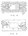
- a third embodiment of a semiconductor integrated circuit according to the present invention is illustrated in Fig. 9.
- the figure shows inside a cavity 34 a layout of lead frames and a bed 36 on which a semiconductor chip is placed.
- an inner lead 32 exclusively used for the ground voltage supply forks two parts in the vicinity of a corner of the cavity 34; one part constitutes an inner lead 32A for the ground voltage Vss1 and the other another inner lead 32B for the ground voltage Vss2.
- An inner lead for the power voltage Vcc is also branched into two inner leads 32D and 32E in the vicinity of a corner of the cavity 34.
- One or two electrode pads may be used for the Vcc supply.
- the branched inner leads 32D and 32E are connected together to the single pad, by means of separate bonding wires.
- Supports 39 respectively fix suspending pins 37 and 38.
- Reenforcing pins 40 fix the inner leads including the inner leads for the power supply, that are laid out in the four corners of the cavity 34, against their displacement from the correct positions.
- FIG. 10 A 4th embodiment of a semiconductor integrated circuit accoridng to the present invention, is illustrated in Fig. 10.
- the figure shows inside a cavity 34 a layout of lead frames and a bed 36 on which a semiconductor chip is placed.
- the 4th embodiment is featured in that a single wide inner lead 32F is used for the ground voltage Vss supply, in place of the inner leads 32A and 32B (Fig. 8).
- An inner lead from the Vcc supply is wider than the other inner leads, as in the second embodiment of Fig. 8.
- FIG. 11 A 5th embodiment of a semiconductor integrated circuit according to the present invention, is illustrated in Fig. 11.
- the figure shows inside a cavity 34 a layout of lead frames and a bed 36 on which a semiconductor chip is placed.
- an inner lead 32A for the Vss1 supply is connected to a suspending pin 38 by a bridge 41.
- Another inner lead 32G is formed connecting to another suspending pin 37.
- the ground voltage Vss1 on the inner lead 32A may be led to the additional inner lead 32G, by way of the bridge 41, pin 38, bed 36, and pin 37. Provision of the inner lead 32G allows use of an additional electrode pad for the Vss supply on the semiconductor chip.
- a 6th embodiment of a semiconductor integrated circuit according to the present invention is illustrativelyed in Fig. 12.
- the figure shows inside a cavity 34 a layout of lead frames and a bed 36 on which a semiconductor chip is placed.
- the number of inner leads below the suspending pin 38 is larger than that above the pin 38.
- Such a pattern that the pin 38 is protruded from the mid portion of the bed 36 as viewed in the height of the bed, as in the Fig. 8 embodiment makes its design difficult, because an imbalance of the layouts of the inner leads with respect to the suspending pin 38, and a mechanical strength of the inner leads thus laid out must be taken into account.
- the suspending pin 38 is protruded from a portion of the bed 36 that is shifted upwardly from the mid portion so that the upper and lower inner leads layouts are well balanced with respect to the suspending pin 38.
- the inner leads for the power voltage Vcc and ground voltage Vss are each configured to have a larger area or to consist of two inner leads.
- the other inner leads than those 32A, 32B and 32C are laid out symmetrically with respect to the suspending pin 38.
- the above pattern of the inner leads reduces cost to design dies by which a lead frame of a metal foil is punched to form such a pattern.
- a 7th embodiment of a semiconductor integrated circuit according to the present invention is shown in Fig. 13.
- a pattern of lead frames for the ground voltages Vss1 and Vss2 and those for signal input/output is illustrated.
- a cavity 34 contains a memory IC chip with two pad electrodes (20, 21) for Vss1 and Vss2 supply (not shown), as in the embodiment of Fig. 6.
- Reference numeral 32 designates inner leads and numeral 3 outer leads respectively continuous to the inner leads 32. The portions of the outer leads 35 extending outside the cavity 34 are properly bent and are to be used as external terminals of the DIP type, as in the previous case.
- the inner lead of the lead frame which is for the ground voltage Vss supply, is branched into two leads 32A and 32B in a portion closer to one side of the cavity 34.
- the inner lead 32A is electrically connected at one end to one of the electrode contacts by a bonding wire (not shown).
- the inner lead 32B is also electrically connected at one end to the other contact by means of another bonding wire (not shown).
- this lead frame is provided not connecting to any of electrode pads on the chip.
- this lead frame consists of a circled dummy inner lead 32H and an outer lead 35H.
- the dummy inner lead 32H is located closer to another side of the cavity 34, and does not extend up to the chip within the cavity 34.
- the ground voltage Vss2 is stable irrespective of the current variation in the output buffer.
- the proper operation of the internal circuit 22 is always ensured.
- the connections using the branched inner leads is advantageous particularly in the recent high speed memory devices, because these require the flow of simultaneous large current into the output buffer. In the high speed memory devices using the above connections, the internal circuit is insensitive to the power noise.
- the instant embodiment uses the dummy inner lead 32H that is located in the end portion of the cavity 34, while failing to reach the chip located in the central portion of the cavity.
- the dummy inner leads 32H With the provision of the dummy inner leads 32H, a more design freedom can be obtained when the inner leads 32A and 32B are designed. If required, larger areas can be secured for these inner leads 32A and 32B.
- FIG. 14 An 8th embodiment of a semiconductor integrated circuit according to the present invention, is illustrated in Fig. 14.
- the figure shows a pattern of lead frames for the ground voltage Vss and those for signal input/output.
- the 8th embodiment is featured in that a single wide inner lead 32F is used for the ground voltage Vss supply, in place of the inner leads 32A and 32B (Fig. 10).
- An inner lead for the Vcc supply is wider than the other inner leads, as in the second embodiment of Fig. 10.
- a dummy lead frame is provided not connecting to any of electrode pads on the chip.
- this lead frame consists of a circled dummy inner lead 32H and an outer lead 35H.
- the dummy inner lead 32H is located closer to another side of the cavity 34, and does not extend up to the chip within the cavity 34.
- Another feature of providing the dummy inner lead 32H located in the end portion of the cavity increases a design freedom in designing the wider inner lead 32F.
- FIG. 15 A 9th embodiment of a semiconductor integrated circuit according to the present invention is shown in Fig. 15.
- a pattern of lead frames for the ground voltages Vss1 and Vss2 and those for signal input/output is illustrated.
- the inner lead of the lead frame which is for the ground voltage Vss supply, is branched into two leads 32A and 32B in a portion closer to one side of the cavity 34.
- a dummy inner lead 32H is also provided.
- This dummy inner lead is coupled with another lead frame 32J for signal input/output that is located adjacent to the dummy inner lead 32H.
- These lead frames are coupled with each other in a portion closer to one side of the cavity 34. The coupling of these lead frames reenforces the inner lead frame 32J for signal input/output.
- a 10th embodiment of a semiconductor integrated circuit according to the present invention is shown in Fig. 16.
- the inner lead of the lead frame which is for the ground voltage Vss supply, is wider than other lead frames.
- a dummy inner lead 32H is also provided. This dummy inner lead is coupled with another lead from 32J for signal input/output that is located adjacent to the dummy inner lead 32H.
- These lead frames are coupled with each other in a portion closer to one side of the cavity 34. The coupling of these lead frames reenforces the inner lead frame 32J for signal input/output.
- the embodiments of Figs. 13 to 16 as mentioned above are each provided with the dummy inner lead 32H.
- the dummy inner lead 32H is formed near the end portion of the cavity, and does not reach the chip located in the central part of the cavity. This feature enables a designer to design the inner lead for the ground voltage supply having a larger area more flexibly.
- the present invention has succeeded in solving the problems of the prior art, the large power noise in the power voltage supply path and the improper operation of the internal circuit due to the power noise.
Landscapes
- Lead Frames For Integrated Circuits (AREA)
- Semiconductor Integrated Circuits (AREA)
Applications Claiming Priority (4)
| Application Number | Priority Date | Filing Date | Title |
|---|---|---|---|
| JP126514/88 | 1988-05-24 | ||
| JP63126514A JPH0666353B2 (ja) | 1988-05-24 | 1988-05-24 | 半導体集積回路 |
| JP324955/88 | 1988-12-23 | ||
| JP63324955A JPH0779150B2 (ja) | 1988-12-23 | 1988-12-23 | 半導体集積回路 |
Publications (2)
| Publication Number | Publication Date |
|---|---|
| EP0343633A2 true EP0343633A2 (fr) | 1989-11-29 |
| EP0343633A3 EP0343633A3 (fr) | 1991-03-06 |
Family
ID=26462692
Family Applications (1)
| Application Number | Title | Priority Date | Filing Date |
|---|---|---|---|
| EP19890109390 Ceased EP0343633A3 (fr) | 1988-05-24 | 1989-05-24 | Circuit intégré semi-conducteur |
Country Status (1)
| Country | Link |
|---|---|
| EP (1) | EP0343633A3 (fr) |
Family Cites Families (5)
| Publication number | Priority date | Publication date | Assignee | Title |
|---|---|---|---|---|
| US4099200A (en) * | 1976-03-26 | 1978-07-04 | Raytheon Company | Package for semiconductor beam lead devices |
| EP0090503A3 (fr) * | 1982-03-25 | 1985-05-22 | Texas Instruments Incorporated | Appareil et procédé pour encapsuler un dispositif semi-conducteur |
| US4680613A (en) * | 1983-12-01 | 1987-07-14 | Fairchild Semiconductor Corporation | Low impedance package for integrated circuit die |
| DE3680265D1 (de) * | 1985-02-28 | 1991-08-22 | Sony Corp | Halbleiterschaltungsanordnung. |
| KR960013630B1 (ko) * | 1986-06-30 | 1996-10-10 | 페어차일드 세미콘덕터 코퍼레이션 | 집적회로에서의 접지 변동 감소 장치 |
-
1989
- 1989-05-24 EP EP19890109390 patent/EP0343633A3/fr not_active Ceased
Also Published As
| Publication number | Publication date |
|---|---|
| EP0343633A3 (fr) | 1991-03-06 |
Similar Documents
| Publication | Publication Date | Title |
|---|---|---|
| US6351040B1 (en) | Method and apparatus for implementing selected functionality on an integrated circuit device | |
| US6593646B2 (en) | Dual die memory | |
| US5229846A (en) | Semiconductor device having noise reducing die pads | |
| US5162894A (en) | Semiconductor integrated circuit having a dummy lead and shaped inner leads | |
| EP0214307A1 (fr) | Dispositif a circuit a semi-conducteurs | |
| US4864164A (en) | Integrated circuit with switching noise reduction by feedback | |
| EP0840375A2 (fr) | Structure d'interconnexion puce-conducteur pour dispositif semi-conducteur | |
| EP0343633A2 (fr) | Circuit intégré semi-conducteur | |
| US7250659B2 (en) | Semiconductor component with ESD protection | |
| US7414300B2 (en) | Molded semiconductor package | |
| JPH05218289A (ja) | 半導体パワー・ダイを保護する方法およびパワー・デバイスのリード部に装着した保護回路 | |
| JP2002353396A (ja) | 半導体集積回路装置 | |
| JP2000049274A (ja) | 半導体装置およびリ―ドフレ―ム | |
| JPH0766370A (ja) | 半導体装置 | |
| KR100635386B1 (ko) | 고속 신호 처리가 가능한 반도체 칩 패키지 | |
| JPH0779150B2 (ja) | 半導体集積回路 | |
| KR930003147B1 (ko) | 반도체 집적회로 | |
| JP2001077230A (ja) | リードフレーム及びそれを用いた半導体装置実装体 | |
| CN100514619C (zh) | 利用下方焊接来定义晶粒功能的集成电路及其制作方法 | |
| JP2919265B2 (ja) | 半導体装置 | |
| KR930005487B1 (ko) | 반도체 장치 | |
| JPH07321283A (ja) | 半導体集積回路および半導体装置 | |
| JPH11307591A (ja) | 半導体装置及びその製造方法、並びにtabテープ | |
| JPS61113267A (ja) | 半導体装置 | |
| JPH0697356A (ja) | 半導体装置 |
Legal Events
| Date | Code | Title | Description |
|---|---|---|---|
| PUAI | Public reference made under article 153(3) epc to a published international application that has entered the european phase |
Free format text: ORIGINAL CODE: 0009012 |
|
| 17P | Request for examination filed |
Effective date: 19890524 |
|
| AK | Designated contracting states |
Kind code of ref document: A2 Designated state(s): DE FR GB |
|
| PUAL | Search report despatched |
Free format text: ORIGINAL CODE: 0009013 |
|
| AK | Designated contracting states |
Kind code of ref document: A3 Designated state(s): DE FR GB |
|
| RHK1 | Main classification (correction) |
Ipc: H01L 23/495 |
|
| 17Q | First examination report despatched |
Effective date: 19921105 |
|
| STAA | Information on the status of an ep patent application or granted ep patent |
Free format text: STATUS: THE APPLICATION HAS BEEN REFUSED |
|
| 18R | Application refused |
Effective date: 19940503 |