EP0343626A2 - Microprocesseur exploitable en un mode de surveillance à redondance fonctionnelle - Google Patents
Microprocesseur exploitable en un mode de surveillance à redondance fonctionnelle Download PDFInfo
- Publication number
- EP0343626A2 EP0343626A2 EP89109380A EP89109380A EP0343626A2 EP 0343626 A2 EP0343626 A2 EP 0343626A2 EP 89109380 A EP89109380 A EP 89109380A EP 89109380 A EP89109380 A EP 89109380A EP 0343626 A2 EP0343626 A2 EP 0343626A2
- Authority
- EP
- European Patent Office
- Prior art keywords
- bus cycle
- signal
- signals
- terminals
- processor
- Prior art date
- Legal status (The legal status is an assumption and is not a legal conclusion. Google has not performed a legal analysis and makes no representation as to the accuracy of the status listed.)
- Granted
Links
Images

Classifications
-
- G—PHYSICS
- G06—COMPUTING OR CALCULATING; COUNTING
- G06F—ELECTRIC DIGITAL DATA PROCESSING
- G06F11/00—Error detection; Error correction; Monitoring
- G06F11/07—Responding to the occurrence of a fault, e.g. fault tolerance
- G06F11/16—Error detection or correction of the data by redundancy in hardware
- G06F11/1629—Error detection by comparing the output of redundant processing systems
- G06F11/1637—Error detection by comparing the output of redundant processing systems using additional compare functionality in one or some but not all of the redundant processing components
-
- G—PHYSICS
- G06—COMPUTING OR CALCULATING; COUNTING
- G06F—ELECTRIC DIGITAL DATA PROCESSING
- G06F11/00—Error detection; Error correction; Monitoring
- G06F11/07—Responding to the occurrence of a fault, e.g. fault tolerance
- G06F11/0703—Error or fault processing not based on redundancy, i.e. by taking additional measures to deal with the error or fault not making use of redundancy in operation, in hardware, or in data representation
- G06F11/0751—Error or fault detection not based on redundancy
- G06F11/0754—Error or fault detection not based on redundancy by exceeding limits
- G06F11/0757—Error or fault detection not based on redundancy by exceeding limits by exceeding a time limit, i.e. time-out, e.g. watchdogs
Definitions
- the present invention relates to a microprocessor and, more particularly, to a microprocessor operable in a functional redundancy monitor (called hereinafter "FRM") mode for supporting a multiple processor system.
- FAM functional redundancy monitor
- a microprocessor As a microprocessor is progressed in performance and function, the application thereof extends to high reliability systems such as an electronic exchanger, an on-line terminal in bank system, a medical apparatus, etc.
- a multiple processor structure is employed, which includes a microprocessor operating in a normal mode and other microprocessor operating in an FRM mode, these microprocessors being interconnected through address, data and control buses along with a system memory and various peripheral units to structure the multiple processor system.
- the normal mode microprocessor operates as a control processing unit of the system. Namely, it drives the buses to output an address, fetches an instruction via the bus, executes the fetched instruction, and drives the buses to read or write operand data.
- the FRM mode microprocessor operates in synchronism with the normal mode microprocessor, but does not drive the buses. Namely, the FRM mode microprocessor simultaneously fetches the same instruction and operand data as those fetched by the normal mode microprocessor and executes the instruction.
- the FRM mode microprocessor also generates internally addresses for fetching the instruction and for reading and writing operand data and operand data to be written, but does not drive the buses by use of the internally generated addresses and operand data.
- the FRM mode microprocessor compares the addresses and data generated by itself with those generated and outputted onto the buses by the normal mode microprocessor, and outputs to the external the comparison resultant as a match signal.
- This match signal takes one logic level when the addresses and data generated by the FRM mode microprocessor are coincident with those generated by the normal mode microprocessor to thereby inform that the normal mode microprocessor operates normally, whereas takes the other logic level when both of then are not coincident with each other to thereby inform that the normal mode microprocessor does not operate normally.
- the FRM mode microprocessor carries out the above-mentioned comparison operation every time a bus cycle is started.
- the logic level of the match signal representative of the comparison resultant in a current bus cycle is held until a next bus cycle is started to obtain the comparison resultant in that cycle. For this reason, if the normal mode microprocessor operates abnormally during the idling period between the adjacent bus cycles or the period of the microprocessor having to be in the operation halt or stop state, the FRM mode microprocessor does not change the match signal to the logic level representative of the maloperation of the normal mode microprocessor during that period. The acknowledgment of the maloperation of the normal mode microprocessor is thereby delayed.
- an object of the present invention is to provide an improved microprocessor operable in an FRM mode.
- Another object is to provide a microprocessor for supporting a multiple processor system in which it is possible to acknowledge a maloperation of a normal mode microprocessor during the above-mentioned period.
- a microprocessor comprises a plurality of terminals to be coupled to another processor to receive external signals generated every bus cycle by the other processor, means for generating internal signals every bus cycle, means for comparing the external signals with the internal signals every bus cycle and for producing a comparison resultant signal after a predetermined time from the beginning of each bus cycle, means for producing an output enable signal during a predetermined period after the predetermined time, a match terminal, and means responsive to the output enable signal for outputting the comparison resultant signal to the match terminal during the predetermined period, wherein after the predetermined period the match terminal is changed to a logic level that represents that the external signals are not coincident with the internal signal.
- the output enable signal is not generated, so that the match terminal is at that logic level. Therefore, if the processor to be monitored activates incorrectly the bus cycle during the bus idling state, the match terminal is at the logic level representative of the misoperation of the processor.
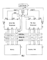
- a multiple processor system includes two processors 1 and 10 according to the present invention.
- These processors 1 and 10 has the same structure as each other, and thus each has a set of data terminals DT connected to a data bus 4, a set of address terminals AT connected to an address bus 3, a set of control terminals CT connected to a control bus 2, a clock terminal 121 supplied with a clock signal CLK from a clock generator 8, a mode designation terminal 108 supplied with an operation mode designation signal NFMD from a system control unit 7, a freeze terminal 120 supplied with an operation freeze signal BFREZ from the unit 7, and a match terminal 117 for outputting a match signal MATCH.
- Further connected to the control, address and data buses 2, 3 and 4 are a memory 5 and peripheral units 6.
- the memory 5 includes a string of instructions for a program to be executed and operand data. Since the processors 1 and 10 are designated to a normal operation mode and an FRM operation mode, respectively, the control unit 7 supplies the NFMD signal of logic "1" to the processor 1 and the NFMD signal of logic "0" to the processor 10. The MATCH signal derived from the terminal 117 of the processor 10 is supplied to the control unit 7, but the terminal 117 of the processor 1 has no connection. Since the processor 1 operates in the normal mode, one of the control signals derived from the control terminals CT thereof, a bus cycle start signal BCYST representative of the start of each bus cycle, is supplied to the control unit 7.
- each of the processors 1 and 10 further has a bus control unit 20 driving the buses 2 to 4, an instruction prefetch unit 21 prefetching instructions, an instruction decoder unit 22 decoding the instruction from the unit 22, an effective address generator calculating and effective address for operand data, and an execution unit 24 executing an instruction on the base of the decoded signals from the unit 22, which are connected as shown.
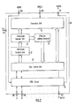
- An FRM circuit 25 is connected between the bus control unit 20 and the control, address and data terminals CT, AT, DT including terminals 105 to 107.
- the FRM circuit 25 electrically connects the control signal output nodes, address signal output nodes and data input and output node of the bus control unit 20 to the corresponding the control, address and data terminals CT, AT and DT.
- the circuit 25 disconnects the control signal output nodes, the address signal output nodes and the data output nodes of the bus control unit 20 from the control, address and data terminals CT, AT and DT with connecting only the data input nodes of the unit 20 to the corresponding data terminals DT, and compares the information outputted from the bus control unit 20 and the information at the terminals CT, AT and DT.
- the comparison resultant signal produced by the circuit 25 is supplied to the terminal 117 and then outputted to the unit 7 as the MATCH signal.
- the normal mode microprocessor 1 generates addresses for fetching an instruction and for reading or writing operand data, drives the buses 2 to 4 to fetch an instruction from the memory 5, executes the fetched instruction and drives the buses 2 to 4 to reach or write operand data from or into the memory 5 or the peripheral units 6.
- the processor 1 thus operates as a central processing unit of the multiple processor system.
- the FRM mode microprocessor 10 generates addresses for fetching an instruction and for reading or writing operand data, fetches an instruction from the memory 5 and operand data from the memory 5 or the peripheral units 6 which are accessed by the normal mode processor 1, executes the fetched instruction and generates operand data to be written into the memory 5 or the peripheral units 6.
- the FRM mode microprocessor 10 does not drive the buses 2 to 3 by use of the control signals, address signals and operand data generated by itself. It compares the control signals, address signals and operand data generated by itself with those generated by the normal mode processor 1 and supplied to the terminals CT, AT and DT via the buses 2 to 3 every time one bus cycle is activated.
- the FRM circuit 25 includes a plurality of circuit units 25-1 to 25-N, each of which is provided for an individual one of the terminals to be monitored. Since each of the units 25-1 to 25-N has the same construction, only the unit 25-1 is shown in detail.
- the unit 25-1 includes a tri-state buffer 140 connected between the output node of the bus control unit 20 and the terminal 105 and controlled by the mode designation signal NFMD. This buffer 140 is activated by the logic "1" of the signal NFMD, so that the output signal from the bus control unit 20 is transferred to the terminal 25.
- the logic "0" of the signal NFMD brings the buffer 104 into a high impedance state, so that the output signal of the unit 20 is not transferred to the terminal 25. Since the terminal 25 is one of the data terminals DT, it is connected to the data input node (not shown) of the bus control unit 20 by a signal line 130. In case where the terminal to be monitored is one of the control and address terminals CT and AT, the line 130 is omitted.
- the terminal 105 is further connected to one input terminal of a 2-input exclusive OR (EX-OR) gate 109 via a series connection of an inverter 150, an N-channel MOS transistor 154 and an inverter 151, and the other input terminal of the EX-OR gate 109 is connected to the output node of the bus control unit 20 via a series connection of an inverter 152, an N-channel MOS transistor 155 and an inverter 153.
- the transistors 154 and 155 are supplied with an inverter signal CLK of the clock signal CLK.
- the EX-OR 109 compares the data signal generated internally with the data signal supplied to the terminal 105.
- the comparison resultant is supplied to an N-channel MOS transistor 113 which is in turn connected between an comparison output node 156 and a grand terminal via an N-channel MOS transistor 112 supplied with the clock signal CLK.
- the output nodes 156 of the units are connected in common to a coincident signal line 111 which is in turn to a power terminal Vcc via an N-channel MOS transistor 100 supplied with the inverter clock signal CLK .
- the transistor 110 and thoses 112 and 113 in each unit constitute a dynamic AND gate which precharges the line 111 during the low level period of the clock signal CLK and samples each comparison resultant of the EX-OR gate 109 during the high level period of the clock signal CLK .
- the transistor 110 may be replaced by a P-channel MOS transistor supplied with the clock signal CLK. Accordingly, when any one of the internally generated signals is not coincident with the corresponding one of the signals at the terminals to be monitored, the corresponding EX-OR gate 109 changes the line 111 to the low level. On the other hand, in case where all the internally generated signals are coincident with the respective ones of the signals at the terminals to be monitored, the line 111 is held at the high level. Since the line 111 has a large stray capacitance, a dynamic wave-shaping circuit 114 shapes the level change on the line 111. The circuit 114 incudes four inverters and two transfer gates connected as shown.
- the output of the circuit 114 is connected to one input node of an AND gate 116 having the other input node supplied via a dynamic delay circuit 115 with the bus cycle start signal 115 which is generated by the unit 20 at the beginning of each bus cycle to inform the start of each bus cycle.
- the delay circuit 15 includes four inverters and three transfer gates connected as shown.
- the output of the AND gate 116 is connected to the terminal 117 and derived as the MATCH signal.
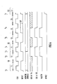
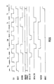
- each bus cycle is constituted of two clocks represented by T1 and T2 states in Fig. 4.
- the normal mode processor 1 fetches an instruction from the memory 5 and executes the same, while the FRM mode processor 10 also fetches the same instruction and executes the same.
- the processor 1 activates a bus cycle B1 for writing the operand data at a timing t1 in synchronism with the leading edge of the clock signal CLK.
- the processor 1 change the bus cycle start signal BCYST to the high level and drives the control, address and data buses by use of the remaining control signals, address signals and operand data signals. These control, address and operand data signals are transferred to the memory 5 and further to the FRM mode processor 10 via the buses 2, 3 and 4.
- the high level of the signal BCYST is held during the T1 state period. Since the FRM mode processor 10 executes the same instruction, it also generates internally the bus cycle start signal BCYST, other control signals, address signals and operand data signals.
- Each of the EX-OR gates 109 compares one of these internally generated signals with the corresponding one of the signals generated by the processor 1 and supplied to the terminals DT, AT and CT of the processor 10 during the low level period of the T1 state.
- the line 111 is precharged to the high level by the transistor 110.
- the comparison resultants derived from the EX-OR gates are sampled by the dynamic AND gate including the transistors 110, 112 and 113 during the high level period of the T2 state.
- the output of the dynamic AND gate is supplied to the circuit 114, so that the output of the circuit 114, i.e. The signal representing whether or not the normal mode processor 1 operates correctly, appears in synchronism with the fall edge (timing t2) of the clock CLK in the T2 state.
- the data comparison part including units 25-1 to 25-N, the transistor 110, the line 111 and the circuit 114 requires one and a half clock times to perform the data comparison from the begining of the bus cycle.
- the output of the circuit 114 takes the high level. This high level is maintained during one clock period.
- the bus cycle start signal BCYST is delayed by the dynamic delay circuit 115 by one and a half clock times. Namely, the circuit 115 change its output to the high level at the timing t2 and holds that level during one clock period.
- the AND gate 116 is made open at the timing t2 and the open state thereof is maintained during one clock period.
- the output of the circuit 114 is transferred onto the terminal 117 at the timing t2 as the MATCH signal. Since the MATCH signal at this time is at the high level, it represents the processor 1 operates correctly.
- the AND gate 16 is closed to change the MATCH signal to the low level at a timing t4.
- the low level of the MATCH signal represents that the processor 1 operates incorrectly.
- the MATCH signal outputted by the FRM mode processor 10 is supplied to the system control unit 7 which are further supplied with the bus cycle start signal BCYST generated by the normal mode processor 1.
- the control unit 7 delays the bus cycle start signal BCYST by one clock and detects the level of the MATCH signals in sychronism with the falling edge of the delayed signal BCYST. Since the MATCH signal is detected to be the high level, the unit 7 judges the microprocessor 1 operates correctly.
- the unit 7 changes the operation freeze signal BFREZ to the active level, so that the operations of the processors 1 and 10 are freezed at this timing.
- the unit 7 gives an alarm or commands the processors 1 and 10 to reexecute the processing operation.
- a next bus cycle B2 is started at a timing t3 continuously with the preceding bus cycle. Assuming that all the signals generated by the processors 1 and 10 are coincident with one another, the MATCH signal is changed to the high level at a timing t5 and returned to the low level at a timing t6.
- a further next bus cycle B3 is not activated continuously with the preceding bus cycle B2, but is activated after two clocks represented as an idling state TI.
- the bus cycle start signal BCYST is not generated and the buses 2 to 4 are not driven by the processor 1.
- the bus cycle start signal BCYST is generated by the processor 1, as shown in Fig. 4 by a dotted line 401.
- the FRM mode processor 10 does not generate internally the bus cycle start signal BCYST, so that the AND gate 116 is maintained in the closed state.
- the MATCH signal is thereby at the low level.
- the bus cycle start signal BCYST generated by the normal mode processor 1 is supplied to the control unit 7. Therefore, the unit 7 delays the supplied signal BCYST by one clock and detects the level of the MATCH signal at the falling edge of the delayed signal BCYST. Since the MATCH signal is detected to be the low level, the operation freeze signal BFREZ is generated at a timing t7. Thus, the immediate acknowledgement of the misoperation of the normal mode processor 1 is carried out not only during the bus cycle period, but also during the bus idling period.
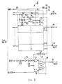
- FIG. 5 there is shown a FRM circuit according to another embodiment of the present invention, in which the same constituents as those shown in Fig. 3 are denoted by the same reference remurals to omit further description thereof.
- a circuit portion including a circuit 24 consisting of two inverters and one transfer gate, a dynamic delay circuit 215 consisting of four inverters and two transfer gates, and a 3-input NAND gate has the same function as the circuit part consisting of the circuits 114 and 116 and the AND gate 116 shown in Fig. 3, and thus produces the comparison resultant signal after one and a half clock times from the start timing point of each bus cycle.
- This comparison resultant signal sets an S-R flip-flop 216 consisting of two NAND gates.
- the set output thereof is supplied to the terminal 117 and derived as the MATCH signal.
- a signal BCYEND is generated by the bus control unit 20 and represents the end of each bus cycle. This signal BCYEND resets the flip-flop 216 to change the MATCH signal to the low level.
- each bus cycle is constituted basically by two clocks represented by T1 and T2 states. However, one or more clocks can be inserted between T1 and T2 states as a wait state TW to enable access to a low speed memory and/or peripheral units.
- the bus cycle end signal BCYEND may used as a sampling signal to be supplied to the control unit 7 in place of the bus cycle start signal BCYST. In this case, the unit 7 detects the level of the MATCH signal in response to the leading edge of the bus cycle end signal BCYEND. Therefore, this circuit also acknowledge immediately the misoperation of the normal mode procesor 1 not only during the bus cycle period, but also bus idling period.
Landscapes
- Engineering & Computer Science (AREA)
- Theoretical Computer Science (AREA)
- Quality & Reliability (AREA)
- Physics & Mathematics (AREA)
- General Engineering & Computer Science (AREA)
- General Physics & Mathematics (AREA)
- Hardware Redundancy (AREA)
- Debugging And Monitoring (AREA)
Applications Claiming Priority (2)
| Application Number | Priority Date | Filing Date | Title |
|---|---|---|---|
| JP128844/88 | 1988-05-25 | ||
| JP63128844A JPH0792764B2 (ja) | 1988-05-25 | 1988-05-25 | マイクロプロセッサ |
Publications (3)
| Publication Number | Publication Date |
|---|---|
| EP0343626A2 true EP0343626A2 (fr) | 1989-11-29 |
| EP0343626A3 EP0343626A3 (fr) | 1991-06-05 |
| EP0343626B1 EP0343626B1 (fr) | 1995-08-30 |
Family
ID=14994783
Family Applications (1)
| Application Number | Title | Priority Date | Filing Date |
|---|---|---|---|
| EP89109380A Expired - Lifetime EP0343626B1 (fr) | 1988-05-25 | 1989-05-24 | Microprocesseur exploitable en un mode de surveillance à redondance fonctionnelle |
Country Status (4)
| Country | Link |
|---|---|
| US (1) | US5136595A (fr) |
| EP (1) | EP0343626B1 (fr) |
| JP (1) | JPH0792764B2 (fr) |
| DE (1) | DE68923995T2 (fr) |
Cited By (1)
| Publication number | Priority date | Publication date | Assignee | Title |
|---|---|---|---|---|
| EP0461792A3 (en) * | 1990-06-12 | 1993-01-13 | Advanced Micro Devices, Inc. | Master/slave checking system |
Families Citing this family (15)
| Publication number | Priority date | Publication date | Assignee | Title |
|---|---|---|---|---|
| US6247144B1 (en) * | 1991-01-31 | 2001-06-12 | Compaq Computer Corporation | Method and apparatus for comparing real time operation of object code compatible processors |
| US5278969A (en) * | 1991-08-02 | 1994-01-11 | At&T Bell Laboratories | Queue-length monitoring arrangement for detecting consistency between duplicate memories |
| JP3063334B2 (ja) * | 1991-12-19 | 2000-07-12 | 日本電気株式会社 | 高信頼度化情報処理装置 |
| GB2268817B (en) * | 1992-07-17 | 1996-05-01 | Integrated Micro Products Ltd | A fault-tolerant computer system |
| US5434997A (en) * | 1992-10-02 | 1995-07-18 | Compaq Computer Corp. | Method and apparatus for testing and debugging a tightly coupled mirrored processing system |
| US5758058A (en) * | 1993-03-31 | 1998-05-26 | Intel Corporation | Apparatus and method for initializing a master/checker fault detecting microprocessor |
| US5392879A (en) * | 1993-04-16 | 1995-02-28 | Otis Elevator Company | Electronic failure detection system |
| US5504859A (en) * | 1993-11-09 | 1996-04-02 | International Business Machines Corporation | Data processor with enhanced error recovery |
| JPH07262148A (ja) * | 1994-03-22 | 1995-10-13 | Nec Corp | コンピュータシステム |
| US5495579A (en) * | 1994-03-25 | 1996-02-27 | Bull Hn Information Systems Inc. | Central processor with duplicate basic processing units employing multiplexed cache store control signals to reduce inter-unit conductor count |
| WO1997022929A1 (fr) * | 1995-12-18 | 1997-06-26 | Elsag International N.V. | Dispositif de verification independante pour processeurs |
| DE19653429C2 (de) * | 1996-12-20 | 1998-10-15 | Siemens Ag | Verfahren zur Überprüfung der Funktionsfähigkeit einer Recheneinheit |
| US5892897A (en) * | 1997-02-05 | 1999-04-06 | Motorola, Inc. | Method and apparatus for microprocessor debugging |
| US6157971A (en) * | 1998-06-02 | 2000-12-05 | Adaptec, Inc. | Source-destination re-timed cooperative communication bus |
| DE102015211458A1 (de) * | 2015-06-22 | 2016-12-22 | Robert Bosch Gmbh | Verfahren und Vorrichtung zum Absichern einer Programmzählerstruktur eines Prozessorsystems und zum Überwachen der Behandlung einer Unterbrechungsanfrage |
Family Cites Families (9)
| Publication number | Priority date | Publication date | Assignee | Title |
|---|---|---|---|---|
| US3783250A (en) * | 1972-02-25 | 1974-01-01 | Nasa | Adaptive voting computer system |
| DE2612100A1 (de) * | 1976-03-22 | 1977-10-06 | Siemens Ag | Digitale datenverarbeitungsanordnung, insbesondere fuer die eisenbahnsicherungstechnik |
| GB2022893B (en) * | 1978-06-10 | 1983-01-12 | Westinghouse Brake & Signal | Fault detection |
| DE2946081C3 (de) * | 1979-11-15 | 1995-09-21 | Wabco Vermoegensverwaltung | Schaltungsanordnung zur Überwachung der Funktion eines Mikroprozessors |
| DE3036856C2 (de) * | 1980-09-30 | 1982-10-28 | Computer Gesellschaft Konstanz Mbh, 7750 Konstanz | Datenverarbeitungsanlage mit zwei Verarbeitungseinheiten |
| US4405983A (en) * | 1980-12-17 | 1983-09-20 | Bell Telephone Laboratories, Incorporated | Auxiliary memory for microprocessor stack overflow |
| US4497059A (en) * | 1982-04-28 | 1985-01-29 | The Charles Stark Draper Laboratory, Inc. | Multi-channel redundant processing systems |
| US4562575A (en) * | 1983-07-07 | 1985-12-31 | Motorola, Inc. | Method and apparatus for the selection of redundant system modules |
| JPH0831049B2 (ja) * | 1986-05-31 | 1996-03-27 | 日本電気株式会社 | ロツクドプロセツサ方式 |
-
1988
- 1988-05-25 JP JP63128844A patent/JPH0792764B2/ja not_active Expired - Fee Related
-
1989
- 1989-05-24 DE DE68923995T patent/DE68923995T2/de not_active Expired - Fee Related
- 1989-05-24 EP EP89109380A patent/EP0343626B1/fr not_active Expired - Lifetime
- 1989-05-24 US US07/356,291 patent/US5136595A/en not_active Expired - Lifetime
Cited By (1)
| Publication number | Priority date | Publication date | Assignee | Title |
|---|---|---|---|---|
| EP0461792A3 (en) * | 1990-06-12 | 1993-01-13 | Advanced Micro Devices, Inc. | Master/slave checking system |
Also Published As
| Publication number | Publication date |
|---|---|
| DE68923995T2 (de) | 1996-04-11 |
| US5136595A (en) | 1992-08-04 |
| EP0343626A3 (fr) | 1991-06-05 |
| JPH0792764B2 (ja) | 1995-10-09 |
| EP0343626B1 (fr) | 1995-08-30 |
| DE68923995D1 (de) | 1995-10-05 |
| JPH01297735A (ja) | 1989-11-30 |
Similar Documents
| Publication | Publication Date | Title |
|---|---|---|
| EP0343626B1 (fr) | Microprocesseur exploitable en un mode de surveillance à redondance fonctionnelle | |
| USRE36766E (en) | Microprocessor breakpoint apparatus | |
| EP0528585B1 (fr) | Système de traitement de données avec antémémoire d'instructions interne | |
| JP3105223B2 (ja) | マイクロコンピュータ,マイクロプロセッサおよびコア・プロセッサ集積回路用デバッグ周辺装置 | |
| US4949241A (en) | Microcomputer system including a master processor and a slave processor synchronized by three control lines | |
| US5987585A (en) | One-chip microprocessor with error detection on the chip | |
| JPH048874B2 (fr) | ||
| RU2137182C1 (ru) | Выполнение инструкции обработки данных | |
| US4926318A (en) | Micro processor capable of being connected with a coprocessor | |
| US5249278A (en) | Microprocessor breakpoint apparatus | |
| JP2586138B2 (ja) | マイクロプロセッサ | |
| JPH0721769B2 (ja) | マイクロプロセッサの冗長構成による機能監視方式 | |
| KR920001100B1 (ko) | 논리연산장치 | |
| US5307482A (en) | Computer, non-maskable interrupt trace routine override | |
| JPS62179033A (ja) | 集積回路マイクロプロセツサ | |
| JPH0159610B2 (fr) | ||
| JP2580558B2 (ja) | インタフェース装置 | |
| EP0382234B1 (fr) | Microprocesseur à mode de surveillance en redondance fonctionnelle | |
| JPS6346460B2 (fr) | ||
| JP2720580B2 (ja) | フォールト・トレラント・コンピュータ | |
| JP2539064B2 (ja) | マイクロプロセッサ | |
| JP2569693B2 (ja) | マイクロコンピュータ | |
| JPH01121965A (ja) | マイクロプロセッサ | |
| JPH05100883A (ja) | データ処理用半導体装置 | |
| SU1501065A1 (ru) | Устройство дл контрол хода программ |
Legal Events
| Date | Code | Title | Description |
|---|---|---|---|
| PUAI | Public reference made under article 153(3) epc to a published international application that has entered the european phase |
Free format text: ORIGINAL CODE: 0009012 |
|
| 17P | Request for examination filed |
Effective date: 19890524 |
|
| AK | Designated contracting states |
Kind code of ref document: A2 Designated state(s): DE FR GB |
|
| PUAL | Search report despatched |
Free format text: ORIGINAL CODE: 0009013 |
|
| AK | Designated contracting states |
Kind code of ref document: A3 Designated state(s): DE FR GB |
|
| 17Q | First examination report despatched |
Effective date: 19931015 |
|
| GRAA | (expected) grant |
Free format text: ORIGINAL CODE: 0009210 |
|
| AK | Designated contracting states |
Kind code of ref document: B1 Designated state(s): DE FR GB |
|
| REF | Corresponds to: |
Ref document number: 68923995 Country of ref document: DE Date of ref document: 19951005 |
|
| ET | Fr: translation filed | ||
| PLBE | No opposition filed within time limit |
Free format text: ORIGINAL CODE: 0009261 |
|
| STAA | Information on the status of an ep patent application or granted ep patent |
Free format text: STATUS: NO OPPOSITION FILED WITHIN TIME LIMIT |
|
| 26N | No opposition filed | ||
| REG | Reference to a national code |
Ref country code: GB Ref legal event code: IF02 |
|
| REG | Reference to a national code |
Ref country code: GB Ref legal event code: 732E |
|
| REG | Reference to a national code |
Ref country code: FR Ref legal event code: TP |
|
| PGFP | Annual fee paid to national office [announced via postgrant information from national office to epo] |
Ref country code: FR Payment date: 20060515 Year of fee payment: 18 |
|
| PGFP | Annual fee paid to national office [announced via postgrant information from national office to epo] |
Ref country code: DE Payment date: 20060518 Year of fee payment: 18 |
|
| PGFP | Annual fee paid to national office [announced via postgrant information from national office to epo] |
Ref country code: GB Payment date: 20060524 Year of fee payment: 18 |
|
| GBPC | Gb: european patent ceased through non-payment of renewal fee |
Effective date: 20070524 |
|
| REG | Reference to a national code |
Ref country code: FR Ref legal event code: ST Effective date: 20080131 |
|
| PG25 | Lapsed in a contracting state [announced via postgrant information from national office to epo] |
Ref country code: DE Free format text: LAPSE BECAUSE OF NON-PAYMENT OF DUE FEES Effective date: 20071201 |
|
| PG25 | Lapsed in a contracting state [announced via postgrant information from national office to epo] |
Ref country code: GB Free format text: LAPSE BECAUSE OF NON-PAYMENT OF DUE FEES Effective date: 20070524 |
|
| PG25 | Lapsed in a contracting state [announced via postgrant information from national office to epo] |
Ref country code: FR Free format text: LAPSE BECAUSE OF NON-PAYMENT OF DUE FEES Effective date: 20070531 |