EP0342279B1 - Plasma apparatus - Google Patents
Plasma apparatus Download PDFInfo
- Publication number
- EP0342279B1 EP0342279B1 EP88304454A EP88304454A EP0342279B1 EP 0342279 B1 EP0342279 B1 EP 0342279B1 EP 88304454 A EP88304454 A EP 88304454A EP 88304454 A EP88304454 A EP 88304454A EP 0342279 B1 EP0342279 B1 EP 0342279B1
- Authority
- EP
- European Patent Office
- Prior art keywords
- specimen
- plasma
- chamber
- specimens
- cassettes
- Prior art date
- Legal status (The legal status is an assumption and is not a legal conclusion. Google has not performed a legal analysis and makes no representation as to the accuracy of the status listed.)
- Expired - Lifetime
Links
- 238000000605 extraction Methods 0.000 claims description 10
- 238000001816 cooling Methods 0.000 claims description 3
- 239000000498 cooling water Substances 0.000 claims description 3
- 238000010438 heat treatment Methods 0.000 claims description 3
- 230000005284 excitation Effects 0.000 claims 1
- 230000032258 transport Effects 0.000 description 6
- 239000004065 semiconductor Substances 0.000 description 5
- VYPSYNLAJGMNEJ-UHFFFAOYSA-N Silicium dioxide Chemical compound O=[Si]=O VYPSYNLAJGMNEJ-UHFFFAOYSA-N 0.000 description 4
- 238000005229 chemical vapour deposition Methods 0.000 description 3
- 238000005530 etching Methods 0.000 description 3
- 238000000034 method Methods 0.000 description 3
- 238000005268 plasma chemical vapour deposition Methods 0.000 description 3
- 230000015572 biosynthetic process Effects 0.000 description 2
- 230000004907 flux Effects 0.000 description 2
- 238000003780 insertion Methods 0.000 description 2
- 230000037431 insertion Effects 0.000 description 2
- 238000004519 manufacturing process Methods 0.000 description 2
- 238000005192 partition Methods 0.000 description 2
- 238000012545 processing Methods 0.000 description 2
- 238000004544 sputter deposition Methods 0.000 description 2
- 229910052581 Si3N4 Inorganic materials 0.000 description 1
- BLRPTPMANUNPDV-UHFFFAOYSA-N Silane Chemical compound [SiH4] BLRPTPMANUNPDV-UHFFFAOYSA-N 0.000 description 1
- 229910052681 coesite Inorganic materials 0.000 description 1
- 238000004891 communication Methods 0.000 description 1
- 229910052906 cristobalite Inorganic materials 0.000 description 1
- 238000005520 cutting process Methods 0.000 description 1
- 230000001419 dependent effect Effects 0.000 description 1
- 230000000694 effects Effects 0.000 description 1
- 239000013013 elastic material Substances 0.000 description 1
- 238000005516 engineering process Methods 0.000 description 1
- 238000009434 installation Methods 0.000 description 1
- 238000012827 research and development Methods 0.000 description 1
- 230000000630 rising effect Effects 0.000 description 1
- 239000000377 silicon dioxide Substances 0.000 description 1
- 235000012239 silicon dioxide Nutrition 0.000 description 1
- 229910052682 stishovite Inorganic materials 0.000 description 1
- 238000012546 transfer Methods 0.000 description 1
- 229910052905 tridymite Inorganic materials 0.000 description 1
Images


Classifications
-
- H—ELECTRICITY
- H01—ELECTRIC ELEMENTS
- H01L—SEMICONDUCTOR DEVICES NOT COVERED BY CLASS H10
- H01L21/00—Processes or apparatus adapted for the manufacture or treatment of semiconductor or solid state devices or of parts thereof
- H01L21/02—Manufacture or treatment of semiconductor devices or of parts thereof
- H01L21/04—Manufacture or treatment of semiconductor devices or of parts thereof the devices having at least one potential-jump barrier or surface barrier, e.g. PN junction, depletion layer or carrier concentration layer
- H01L21/18—Manufacture or treatment of semiconductor devices or of parts thereof the devices having at least one potential-jump barrier or surface barrier, e.g. PN junction, depletion layer or carrier concentration layer the devices having semiconductor bodies comprising elements of Group IV of the Periodic System or AIIIBV compounds with or without impurities, e.g. doping materials
- H01L21/20—Deposition of semiconductor materials on a substrate, e.g. epitaxial growth solid phase epitaxy
- H01L21/205—Deposition of semiconductor materials on a substrate, e.g. epitaxial growth solid phase epitaxy using reduction or decomposition of a gaseous compound yielding a solid condensate, i.e. chemical deposition
-
- H—ELECTRICITY
- H01—ELECTRIC ELEMENTS
- H01L—SEMICONDUCTOR DEVICES NOT COVERED BY CLASS H10
- H01L21/00—Processes or apparatus adapted for the manufacture or treatment of semiconductor or solid state devices or of parts thereof
- H01L21/67—Apparatus specially adapted for handling semiconductor or electric solid state devices during manufacture or treatment thereof; Apparatus specially adapted for handling wafers during manufacture or treatment of semiconductor or electric solid state devices or components ; Apparatus not specifically provided for elsewhere
- H01L21/677—Apparatus specially adapted for handling semiconductor or electric solid state devices during manufacture or treatment thereof; Apparatus specially adapted for handling wafers during manufacture or treatment of semiconductor or electric solid state devices or components ; Apparatus not specifically provided for elsewhere for conveying, e.g. between different workstations
- H01L21/67739—Apparatus specially adapted for handling semiconductor or electric solid state devices during manufacture or treatment thereof; Apparatus specially adapted for handling wafers during manufacture or treatment of semiconductor or electric solid state devices or components ; Apparatus not specifically provided for elsewhere for conveying, e.g. between different workstations into and out of processing chamber
- H01L21/67751—Apparatus specially adapted for handling semiconductor or electric solid state devices during manufacture or treatment thereof; Apparatus specially adapted for handling wafers during manufacture or treatment of semiconductor or electric solid state devices or components ; Apparatus not specifically provided for elsewhere for conveying, e.g. between different workstations into and out of processing chamber vertical transfer of a single workpiece
-
- H—ELECTRICITY
- H01—ELECTRIC ELEMENTS
- H01J—ELECTRIC DISCHARGE TUBES OR DISCHARGE LAMPS
- H01J37/00—Discharge tubes with provision for introducing objects or material to be exposed to the discharge, e.g. for the purpose of examination or processing thereof
- H01J37/32—Gas-filled discharge tubes
- H01J37/32009—Arrangements for generation of plasma specially adapted for examination or treatment of objects, e.g. plasma sources
- H01J37/32018—Glow discharge
-
- H—ELECTRICITY
- H01—ELECTRIC ELEMENTS
- H01L—SEMICONDUCTOR DEVICES NOT COVERED BY CLASS H10
- H01L21/00—Processes or apparatus adapted for the manufacture or treatment of semiconductor or solid state devices or of parts thereof
- H01L21/67—Apparatus specially adapted for handling semiconductor or electric solid state devices during manufacture or treatment thereof; Apparatus specially adapted for handling wafers during manufacture or treatment of semiconductor or electric solid state devices or components ; Apparatus not specifically provided for elsewhere
- H01L21/67005—Apparatus not specifically provided for elsewhere
- H01L21/67011—Apparatus for manufacture or treatment
- H01L21/67017—Apparatus for fluid treatment
- H01L21/67063—Apparatus for fluid treatment for etching
- H01L21/67069—Apparatus for fluid treatment for etching for drying etching
-
- H—ELECTRICITY
- H01—ELECTRIC ELEMENTS
- H01L—SEMICONDUCTOR DEVICES NOT COVERED BY CLASS H10
- H01L21/00—Processes or apparatus adapted for the manufacture or treatment of semiconductor or solid state devices or of parts thereof
- H01L21/67—Apparatus specially adapted for handling semiconductor or electric solid state devices during manufacture or treatment thereof; Apparatus specially adapted for handling wafers during manufacture or treatment of semiconductor or electric solid state devices or components ; Apparatus not specifically provided for elsewhere
- H01L21/67005—Apparatus not specifically provided for elsewhere
- H01L21/67011—Apparatus for manufacture or treatment
- H01L21/67155—Apparatus for manufacturing or treating in a plurality of work-stations
- H01L21/6719—Apparatus for manufacturing or treating in a plurality of work-stations characterized by the construction of the processing chambers, e.g. modular processing chambers
-
- H—ELECTRICITY
- H01—ELECTRIC ELEMENTS
- H01L—SEMICONDUCTOR DEVICES NOT COVERED BY CLASS H10
- H01L21/00—Processes or apparatus adapted for the manufacture or treatment of semiconductor or solid state devices or of parts thereof
- H01L21/67—Apparatus specially adapted for handling semiconductor or electric solid state devices during manufacture or treatment thereof; Apparatus specially adapted for handling wafers during manufacture or treatment of semiconductor or electric solid state devices or components ; Apparatus not specifically provided for elsewhere
- H01L21/67005—Apparatus not specifically provided for elsewhere
- H01L21/67011—Apparatus for manufacture or treatment
- H01L21/67155—Apparatus for manufacturing or treating in a plurality of work-stations
- H01L21/67196—Apparatus for manufacturing or treating in a plurality of work-stations characterized by the construction of the transfer chamber
-
- H—ELECTRICITY
- H01—ELECTRIC ELEMENTS
- H01L—SEMICONDUCTOR DEVICES NOT COVERED BY CLASS H10
- H01L21/00—Processes or apparatus adapted for the manufacture or treatment of semiconductor or solid state devices or of parts thereof
- H01L21/67—Apparatus specially adapted for handling semiconductor or electric solid state devices during manufacture or treatment thereof; Apparatus specially adapted for handling wafers during manufacture or treatment of semiconductor or electric solid state devices or components ; Apparatus not specifically provided for elsewhere
- H01L21/67005—Apparatus not specifically provided for elsewhere
- H01L21/67011—Apparatus for manufacture or treatment
- H01L21/67155—Apparatus for manufacturing or treating in a plurality of work-stations
- H01L21/67207—Apparatus for manufacturing or treating in a plurality of work-stations comprising a chamber adapted to a particular process
-
- H—ELECTRICITY
- H01—ELECTRIC ELEMENTS
- H01L—SEMICONDUCTOR DEVICES NOT COVERED BY CLASS H10
- H01L21/00—Processes or apparatus adapted for the manufacture or treatment of semiconductor or solid state devices or of parts thereof
- H01L21/67—Apparatus specially adapted for handling semiconductor or electric solid state devices during manufacture or treatment thereof; Apparatus specially adapted for handling wafers during manufacture or treatment of semiconductor or electric solid state devices or components ; Apparatus not specifically provided for elsewhere
- H01L21/677—Apparatus specially adapted for handling semiconductor or electric solid state devices during manufacture or treatment thereof; Apparatus specially adapted for handling wafers during manufacture or treatment of semiconductor or electric solid state devices or components ; Apparatus not specifically provided for elsewhere for conveying, e.g. between different workstations
- H01L21/67763—Apparatus specially adapted for handling semiconductor or electric solid state devices during manufacture or treatment thereof; Apparatus specially adapted for handling wafers during manufacture or treatment of semiconductor or electric solid state devices or components ; Apparatus not specifically provided for elsewhere for conveying, e.g. between different workstations the wafers being stored in a carrier, involving loading and unloading
- H01L21/67778—Apparatus specially adapted for handling semiconductor or electric solid state devices during manufacture or treatment thereof; Apparatus specially adapted for handling wafers during manufacture or treatment of semiconductor or electric solid state devices or components ; Apparatus not specifically provided for elsewhere for conveying, e.g. between different workstations the wafers being stored in a carrier, involving loading and unloading involving loading and unloading of wafers
Definitions
- the present invention relates to a plasma apparatus utilizing electron cyclotron resonance used as a CVD (chemical vapor deposition) apparatus, an etching apparatus, a sputtering apparatus or the like for manufacturing semiconductor equipments, and more particularly to a plasma apparatus using a specimen chamber in common with respect to two plasma generation chambers.
- CVD chemical vapor deposition
- the plasma apparatus utilizing electron cyclotron resonance (to be hereinafter referred to as ECR) is advantageous in that plasma of high activity can be obtained under low gas pressure, the ion energy can widely be selected, a large ion current is obtained, and an ion flow is superior in directivity and uniformity, and has been promoted in research and development as the apparatus indispensable for manufacture of a high integrated semiconductor apparatus.
- ECR electron cyclotron resonance
- Fig. 1 is a longitudinally sectional view of the conventional plasma apparatus of the type as described in JOURNAL OF VACUUM SCIENCE & TECHNOLOGY B, vol. 4, no. 3, May/June 1986, pages 696-700, American Vacuum Society, Woodbury, New York, US; T. ONO et al.: "Reactive ion stream etching utilizing electron cyclotron resonance plasma", utilizing the ECR as the plasma CVD apparatus, in which a plasma generation chamber 31 is shown.
- the plasma generation chamber 31 is surrounded with double framed walls and provided therebetween with a cooling water flow chamber 31a, at the center of the upper wall with a microwave inlet 31c vacuum-sealed by a quartz glass plate 31b, and at the center of the lower wall with a plasma extraction window 31d opposite to the microwave inlet 31c.
- a wave guide 32 is connected at one end thereof with the microwave inlet 31c, a reaction chamber 33 as specimen chamber is provided and faces the plasma extraction window 31d, and exciting coils 34 are disposed around and coaxially with the plasma generation chamber 31 and an end portion of the wave guide 32 connected thereto.
- the waveguide 32 is connected at the other end thereof with a high frequency oscillator (not shown), in the reaction chamber 33 is disposed a specimen table 36 for a specimen S of a semiconductor wafer or the like opposite to the plasma extraction window 31d, and an evacuation port 33a communicating with an evacuation system 37 is open at a lower wall of the reaction chamber 33.
- reference numerals 31e and 31f designate a supply system for cooling water and a drain system therefor respectively and 31g designates a gas supply system.
- the specimen S is placed on the specimen table 36, gas is introduced into the plasma generation chamber 31 through a primary gas supply system 31g, D.C. voltage is applied to the exciting coils 34, and microwave power is introduced into the plasma chamber 31 through the waveguide 32, so that plasma is generated in the plasma generation chamber 31.
- the generated plasma is incident on the specimen S in the reaction chamber 33 by means of a divergent magnetic field generated by the exciting coils 34 and lowered of the magnetic flux density from the plasma extraction window 31d toward the reaction chamber 33 thereunder, thereby plasma-decomposing the gas in the reaction chamber 33 to form a semiconductor film or the like on the surface of the specimen S.
- the plasma apparatus When semiconductor films are formed on many specimens by such the apparatus respectively, the plasma apparatus of course increases in number corresponding to the number of specimens. As a result, the problem is created in that it is much useless in equipment to increase the plasma apparatus independently and an installation space is liable to be wasted.
- the present invention has been designed.
- a first object thereof is to provide a plasma apparatus which uses a specimen chamber in common with respect to two plasma generation chambers so as to be compact as a whole.
- a second object of the invention is to provide a plasma apparatus which disposes a load lock chamber communicating with the specimen chamber, contains specimens in cassettes disposed in the load lock chamber, and transports the specimens by transport means between the load lock chamber and the specimen chamber, whereby a rest time is reducible and an efficient specimen processing is performable.
- a third object of the invention is to provide a plasma apparatus which is provided at the load lock chamber with cassettes loading thereon a plurality of specimens so that the specimens together with the cassettes are taken in or out of the load lock chamber, thereby facilitating treatment of the specimen.
- a fourth object of the invention is to provide a plasma apparatus which contains a plurality of specimens in the cassettes in the load lock chamber and processes them, whereby the number of times of gas supply and evacuation works with respect to the load lock chamber is largely reduced, a running cost is expected to be lower, and the work efficiency is improved.
- the first object is achieved by the plasma apparatus according to the invention as disclosed in Claim 1.
- the dependent claims describe particular embodiments of the invention.
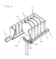
- reference numeral 1, 1 designate plasma generation chambers
- 2, 2 designate waveguides
- 3 designates a reaction chamber as a specimen chamber for applying a film on a specimen
- 4 designate exciting coils
- 5 designates a load lock chamber.
- the plasma generation chambers 1, 1 are cylindrical, spaced at a predetermined interval from each other, with the axis thereof being horizontal and in alignment with each other.
- the reaction chamber 3 as the specimen chamber in common to both the plasma generation chambers 1, 1 is provided therebetween, and under the plasma generation chambers 1, 1 and reaction chamber 3 is provided a load lock chamber 5 connected with the reaction chamber 3 through two communicating conduits for communicating or cutting off into airtight condition by operating gate valves 11, 11.
- Microwave inlets 1c, 1c sealed by quartz glass plates 1b, 1b are provided at the centers of outside walls of the plasma generation chambers 1, 1 respectively and plasma extraction windows 1d, 1d are open at the centers of the inside walls of the same and opposite to each other across the reaction chamber 3 respectively.
- the microwave inlets 1c, 1c connect with one ends of the waveguides 2, 2, the exciting coils 4, 4 being provided coaxially around the plasma generation chambers 1, 1 and the end portions of the waveguides 2, 2 connected thereto respectively.
- the waveguides 2, 2 are connected at the other ends to high frequency oscillators (not shown) so that the microwaves generated therefrom are introduced into the respective plasma generation chambers 1, 1 through the waveguides 2, 2 and microwave inlets 1c, 1c.
- the exciting coils 4, 4 disposed as above-mentioned are positioned coaxially with the plasma generation chambers 1, 1 and waveguides 2, 2 and in alignment with each other and connected to a D.C.power source (not shown), so that the magnetic field is generated by introducing the microwave into each of the plasma generation chambers 1, 1 so as to generate plasma, and the divergent magnetic field lowering its magnetic flux density toward the reaction chamber 3 is produced in each of the plasma generation chambers 1, 1, whereby the plasma is incident to the reaction chamber 3.
- Each of the cassettes 6, 6, as shown in Fig. 3, is open upwardly and has at the bottom an opening extending lengthwise of the cassette 6 and having a width smaller than a diameter of the specimen S, thereby being formed in a hollow rectangular parallelepiped provided with an insertion bore 6a through which each of the holders 8h, 8h of the loader 8 is passable.
- a plurality of partition ribs 6b, 6b,... extending vertically, opposite to each other, and spaced at predetermined intervals lengthwise of the side plates, so that the specimens S, S,... are housed one by one in the intervals between the adjacent partition ribs 6b, 6b ....
- each of the cassettes 6, 6 is placed on each guide tables 7a, 7a on a guide rail 7 disposed in the cassette housing 5a and extending lengthwise thereof, each of the guide tables 7a, 7a engaging with a screw rod 7c by a ball screw through each of the connecting rods 7b, 7b.
- each of the table 7a, 7a in turn, each of the cassettes 6, 6 is driven by a motor M provided at one end of the screw rod 7c and moved one by one pitch corresponding to the interval between the respective specimens S, S contained in each of the cassettes 6, 6, thereby being positioned opposite to each of the holder 8h, 8h of the loader 8.
- the loader 8 is so constructed that a cylinder 8a erected at the center of the housing 5b connects at the upper and lower ends with air supply and exhaust pipes 8b and 8c respectively, the cylinder 8a being provided therein with a piston 8d of magnet and at the outer surface with blocks 8e carrying the holders 8h, 8h and slidably mounted on the cylinder 8a.
- Air is supplied or exhausted into or out of the cylinder 8a through the air supply and exhaust pipes 8b and 8c, whereby the piston 8d, in turn the block 8e magnetically attracted thereto, are vertically moved to move vertically between the housing 5a at the load lock chamber 5 and the reaction chamber 3 the holders 8h, 8h supported to the block 8e through support rods 8f, 8f and support bars 8g, 8g respectively.
- Each of the holders 8h, 8h, as shown in Figs. 3 and 4 is formed on the upper end of each of the support bars 8g, 8g, of a length somewhat smaller than a diameter of each specimen S, and provided with a groove 8i of a circular arc and about equal in the size to the edge of each specimen S.
- the holders 8h, 8h when moved upwardly through the cassettes 6, 6 due to the rising of the block 8e, hold the specimens S fitted at the lower edges into the grooves 8i, 8i and rise through the gate valves 11, 11 to the position in the reaction chamber 3 where the specimens S are delivered to the clamps 10, 10 as the first transfer means. On the contrary, the holders 8h, 8h receive the specimens S from the clamps 10, 10 and return the same to the cassettes 6, 6 on the way downward.
- Each specimen mount 9 is formed in a disk larger in diameter than the specimen S, fixed at the center of the rear surface thereof to both lengthwise ends of a rod 9a, and supported to the upper wall of the reaction chamber 3 through a support 9b in relation of being opposite to the plasma extraction window 1d at each plasma generation chamber 1, the specimen S being adapted to be electrostatically attracted (alternatively it may be fixed by mechanical means) to the front surface of each specimen mount 9.
- Each of the specimen mount 9, 9 is provided with cooling and heating means for the specimen S and adapted to be moved toward or away from each plasma extraction window 1d by expanding or contracting the rod 9a.
- each of them is so constructed that each rod 10b of each air 10a cylinder 10a fixed to the outer surface of the wall of the reaction chamber 3 projects thereinto and an actuator 10c is attached to the utmost end of the rod 10b, so that each air cylinder operates to move each clamp arm 10d in reciprocation between the delivery position of specimen S shown by the solid line in Fig. 2 and that shown by the one-dot chain line in respect to each of the specimen mounts 9, 9 in the same drawing.
- the actuators 10c, 10c open or close the clamp arms 10d, 10d at the respective positions, and the clamp arms 10d, 10d grip the specimens S through elastic materials 10e, 10e or release it, thereby delivering the specimens S between the respective the holders 8h, 8h of the loader 8 and specimen mounts 9, 9 respectively.
- the gate valves 11, 11 are closed, gas is supplied into the load lock chamber 5 from the feed and evacuation system therein (not shown) so as to approximately equalize the gas pressure with the atmospheric pressure, thereafter the exchange port is open to draw out cassettes 6, 6, and new cassettes 6, 6 are loaded on the guided tables 7a, 7a which are put on the guide rail 7.
- the exchange port is closed and the gas is evacuated through the evacuation system (not shown) so that the inside of the load lock chamber 5 is set to a predetermined degree of vacuum about equal to that in the reaction chamber 3, and thereafter the gate valves 11, 11 are set to be open and the loader 8 is actuated.
- air is supplied in to the cylinder 8a from the lower end thereof and exhausted through the upper end so as to raise the piston 8d, blocks 8e and holders 8h, 8h coupled therewith, the holders 8h, 8h are inserted into the cassettes 6, 6 through the insertion bores 6a, 6a at the bottoms respectively, the specimens S, while being fitted at the lower edges into the grooves 8i, 8i, are picked up from the cassettes 6, 6 and raised to the delivery positions in the reaction chamber 3 respectively through the communication conduits and then stop.
- the clamps 10, 10 as first transport means are stand-by while keeping both the clamp arms 10d, 10d open, so that, when the loader 8 stops its rise, the actuators 10c, 10c operate to close the respective clamp arms 10d, 10d and the elastic members 10e, 10e, as shown in Fig. 4, clamp therebetween the specimen S. Then, the loader 8 lowers and returns to the original position and the gate valves 11, 11 are closed. Also, the clamps 10, 10 move toward the respective specimen mounts 9, 9, the specimen S is electrostatically attracted thereto, and the respective clamp arms 10d, 10d are released to return to the original position for stand-by.
- Gas is supplied into the plasma generation chamber 1, 1 through the gas supply system (not shown), a D.C. current is flowed in the exciting coils 4, 4, microwave is introduced into the plasma generation chambers 1, 1 through the waveguide 2, 2 to generate plasma, the generated plasma is incident around the specimens S in the reaction chamber 3 by means of the divergent magnetic field generated by the exciting coils 4, 4, and the source gas, for example, SiH4, O2 or N2, supplied from the gas supply system (not shown) is plasma-decomposed, thereby applying on the surface of specimen S a film of SiO2, Si3N4 or the like.
- the source gas for example, SiH4, O2 or N2 supplied from the gas supply system (not shown) is plasma-decomposed, thereby applying on the surface of specimen S a film of SiO2, Si3N4 or the like.
- the clamps 10, 10 move close to the respective front surfaces of specimen mounts 9, 9 and close the clamp arms 10d, 10d to hold the specimens S thereby and then moves forward to the delivery position.
- the gate valves 11, 11 are open, the loader 8 again rises to the position where the specimen S at the lower edge is fitted into the groove 8i at the holder 8h, then the clamp arms 10d, 10d are released, and the specimen S is transferred to the loader 8.
- the leader 8 lowers to the original position and the film-applied specimen is reduced into the respective cassettes 6, 6.
- the pitch feeding motor M is driven to move the cassettes 6, 6 in the direction of the arrow so as to load the next specimens S on the holders 8h, 8h, the loader 8 again rises to pick up the specimens S from the cassettes 6, 6 and further rises to the delivery position in the reaction chamber 3 to deliver the specimens S to the clamps 10, 10 respectively.
- the embodiment applies the invention to the CVD apparatus, the invention is not limited thereto, but of course applicable to, for example, an etching apparatus or a sputtering apparatus.
- the plasma apparatus of the invention uses only one specimen chamber to be compact, can process simultaneously two specimens so as to raise the process efficiency, houses a plurality of specimens in the load lock chamber and completes the processing of them, and thereafter takes the specimens together with the cassettes from or into the load lock chamber, thereby facilitating handling of the specimens, largely reducing the gas supply and exhaust works with respect to the load lock chamber, saving a running cost, and improving the work efficiency.
Priority Applications (1)
| Application Number | Priority Date | Filing Date | Title |
|---|---|---|---|
| DE8888304454T DE3870445D1 (de) | 1987-03-30 | 1988-05-17 | Plasmageraet. |
Applications Claiming Priority (1)
| Application Number | Priority Date | Filing Date | Title |
|---|---|---|---|
| JP62078776A JPS63244619A (ja) | 1987-03-30 | 1987-03-30 | プラズマ装置 |
Publications (2)
| Publication Number | Publication Date |
|---|---|
| EP0342279A1 EP0342279A1 (en) | 1989-11-23 |
| EP0342279B1 true EP0342279B1 (en) | 1992-04-22 |
Family
ID=13671303
Family Applications (1)
| Application Number | Title | Priority Date | Filing Date |
|---|---|---|---|
| EP88304454A Expired - Lifetime EP0342279B1 (en) | 1987-03-30 | 1988-05-17 | Plasma apparatus |
Country Status (5)
| Country | Link |
|---|---|
| US (1) | US4902934A (ja) |
| EP (1) | EP0342279B1 (ja) |
| JP (1) | JPS63244619A (ja) |
| KR (1) | KR920006263B1 (ja) |
| DE (1) | DE3870445D1 (ja) |
Families Citing this family (28)
| Publication number | Priority date | Publication date | Assignee | Title |
|---|---|---|---|---|
| JPH01134927A (ja) * | 1987-11-20 | 1989-05-26 | Nippon Telegr & Teleph Corp <Ntt> | プラズマ処理装置 |
| US5227695A (en) * | 1989-06-05 | 1993-07-13 | Centre National De La Recherche Scientifique | Device for coupling microwave energy with an exciter and for distributing it therealong for the purpose of producing a plasma |
| JP2644912B2 (ja) | 1990-08-29 | 1997-08-25 | 株式会社日立製作所 | 真空処理装置及びその運転方法 |
| US7089680B1 (en) | 1990-08-29 | 2006-08-15 | Hitachi, Ltd. | Vacuum processing apparatus and operating method therefor |
| USRE39756E1 (en) * | 1990-08-29 | 2007-08-07 | Hitachi, Ltd. | Vacuum processing operating method with wafers, substrates and/or semiconductors |
| USRE39824E1 (en) * | 1990-08-29 | 2007-09-11 | Hitachi, Ltd. | Vacuum processing apparatus and operating method with wafers, substrates and/or semiconductors |
| US5200232A (en) * | 1990-12-11 | 1993-04-06 | Lam Research Corporation | Reaction chamber design and method to minimize particle generation in chemical vapor deposition reactors |
| DE9102438U1 (ja) * | 1991-03-01 | 1992-06-25 | Roehm Gmbh, 6100 Darmstadt, De | |
| JP2532401Y2 (ja) * | 1991-04-16 | 1997-04-16 | ソニー株式会社 | バイアスecrプラズマcvd装置 |
| DE69204670T2 (de) * | 1991-05-21 | 1996-04-18 | Materials Research Corp | Sanftaetz-einheit fuer modulare bearbeitungsanlagen und ecr-plasmaerzeuger fuer eine solche einheit. |
| JP3042127B2 (ja) * | 1991-09-02 | 2000-05-15 | 富士電機株式会社 | 酸化シリコン膜の製造方法および製造装置 |
| US5343885A (en) * | 1992-03-04 | 1994-09-06 | Baxter International Inc. | Vacuum air lock for a closed perimeter solvent conservation system |
| JP3194022B2 (ja) * | 1992-07-06 | 2001-07-30 | 東京エレクトロン株式会社 | プラズマ表面処理の制御装置 |
| US5352487A (en) * | 1992-08-31 | 1994-10-04 | Gte Products Corporation | Process for the formation of SiO2 films |
| DE4310258A1 (de) * | 1993-03-30 | 1994-10-06 | Bosch Gmbh Robert | Vorrichtung zur Herstellung einer Plasmapolymerschutzschicht auf Werkstücken, insbesondere Scheinwerferreflektoren |
| USRE39353E1 (en) * | 1994-07-21 | 2006-10-17 | Applera Corporation | Mass spectrometer system and method for matrix-assisted laser desorption measurements |
| US5633502A (en) * | 1995-08-11 | 1997-05-27 | E. A. Fischione Instruments, Inc. | Plasma processing system for transmission electron microscopy specimens and specimen holders |
| DE19541236A1 (de) * | 1995-11-06 | 1997-05-07 | Leybold Ag | Vorrichtung zum Beschichten der Oberflächen von als Rotationskörper ausgeformten Substraten |
| US5897711A (en) * | 1995-12-22 | 1999-04-27 | Lam Research Corporation | Method and apparatus for improving refractive index of dielectric films |
| US6042901A (en) * | 1996-02-20 | 2000-03-28 | Lam Research Corporation | Method for depositing fluorine doped silicon dioxide films |
| US6152070A (en) * | 1996-11-18 | 2000-11-28 | Applied Materials, Inc. | Tandem process chamber |
| US5869149A (en) * | 1997-06-30 | 1999-02-09 | Lam Research Corporation | Method for preparing nitrogen surface treated fluorine doped silicon dioxide films |
| EP1209721B1 (en) | 1997-10-10 | 2007-12-05 | European Community | Inductive type plasma processing chamber |
| US6071573A (en) * | 1997-12-30 | 2000-06-06 | Lam Research Corporation | Process for precoating plasma CVD reactors |
| US6873113B2 (en) * | 2000-04-13 | 2005-03-29 | Tokyo Electron Limited | Stand alone plasma vacuum pump |
| US6729850B2 (en) | 2001-10-31 | 2004-05-04 | Tokyo Electron Limited | Applied plasma duct system |
| EP2141739A3 (en) * | 2008-06-30 | 2011-01-12 | Intevac, Inc. | System and method for substrate transport |
| US9157145B2 (en) | 2008-07-29 | 2015-10-13 | Intevac, Inc. | Processing tool with combined sputter and evaporation deposition sources |
Family Cites Families (7)
| Publication number | Priority date | Publication date | Assignee | Title |
|---|---|---|---|---|
| US4550239A (en) * | 1981-10-05 | 1985-10-29 | Tokyo Denshi Kagaku Kabushiki Kaisha | Automatic plasma processing device and heat treatment device |
| DE3244391A1 (de) * | 1982-12-01 | 1984-06-07 | Leybold-Heraeus GmbH, 5000 Köln | Vorrichtung zur beschichtung von substraten durch plasmapolymerisation |
| GB8418063D0 (en) * | 1984-07-16 | 1984-08-22 | Atomic Energy Authority Uk | Temperature control in vacuum |
| US4668365A (en) * | 1984-10-25 | 1987-05-26 | Applied Materials, Inc. | Apparatus and method for magnetron-enhanced plasma-assisted chemical vapor deposition |
| US4641060A (en) * | 1985-02-11 | 1987-02-03 | Applied Microwave Plasma Concepts, Inc. | Method and apparatus using electron cyclotron heated plasma for vacuum pumping |
| JPS6276137A (ja) * | 1985-09-30 | 1987-04-08 | Hitachi Ltd | イオン源 |
| FR2614041B1 (fr) * | 1987-04-14 | 1989-06-30 | Guy Mongodin | Procede et appareil pour le traitement de substrats en faisant intervenir un faisceau d'ions acceleres pour l'erosion de ces substrats, ou pour le depot d'une ou plusieurs couches de revetement |
-
1987
- 1987-03-30 JP JP62078776A patent/JPS63244619A/ja active Pending
-
1988
- 1988-05-10 US US07/192,130 patent/US4902934A/en not_active Expired - Fee Related
- 1988-05-17 DE DE8888304454T patent/DE3870445D1/de not_active Expired - Lifetime
- 1988-05-17 EP EP88304454A patent/EP0342279B1/en not_active Expired - Lifetime
- 1988-06-17 KR KR1019880007307A patent/KR920006263B1/ko not_active IP Right Cessation
Also Published As
| Publication number | Publication date |
|---|---|
| KR920006263B1 (ko) | 1992-08-01 |
| JPS63244619A (ja) | 1988-10-12 |
| KR900001280A (ko) | 1990-01-31 |
| US4902934A (en) | 1990-02-20 |
| EP0342279A1 (en) | 1989-11-23 |
| DE3870445D1 (de) | 1992-05-27 |
Similar Documents
| Publication | Publication Date | Title |
|---|---|---|
| EP0342279B1 (en) | Plasma apparatus | |
| US4851101A (en) | Sputter module for modular wafer processing machine | |
| US5342472A (en) | Plasma processing apparatus | |
| EP0161927B1 (en) | Load lock pumping mechanism | |
| JPH05166757A (ja) | 被処理体の温調装置 | |
| KR101334758B1 (ko) | 기판 처리 장치 및 반도체 장치의 제조 방법 | |
| JP2000195925A (ja) | 基板処理装置 | |
| KR100321325B1 (ko) | 플라즈마생성방법및장치와그것을사용한플라즈마처리방법및장치 | |
| US20020121345A1 (en) | Multi-chamber system for semiconductor process | |
| EP0653775A1 (en) | Microwave plasma processing apparatus and method | |
| KR970072001A (ko) | 멀티덱 웨이퍼 처리 시스템 | |
| JP2010532565A (ja) | 単一の平面アンテナを備えた誘導結合二重ゾーン処理チャンバ | |
| KR20180125433A (ko) | 진공 시스템에서 마스크 디바이스를 핸들링하는 방법들, 마스크 핸들링 장치, 및 진공 시스템 | |
| JPH03136345A (ja) | 半導体ウエーハ処理装置 | |
| US20180076075A1 (en) | Semiconductor process equipment | |
| US5203981A (en) | Vacuum-treatment apparatus | |
| CA1300357C (en) | Method and apparatus for handling and processing wafer-like materials | |
| US6261428B1 (en) | Magnetron plasma process apparatus | |
| US20210375596A1 (en) | Apparatus for treating substrate | |
| KR102378330B1 (ko) | 기판 처리 장치 및 기판 처리 방법 | |
| JPS62204515A (ja) | 試料の搬送装置 | |
| JPH08181183A (ja) | 試料の搬送装置 | |
| KR20240011013A (ko) | 기판 처리 장치 | |
| JPH01120811A (ja) | 半導体ウエハ処理装置 | |
| CN116364630A (zh) | 支承单元和具有支承单元的用于处理基板的装置 |
Legal Events
| Date | Code | Title | Description |
|---|---|---|---|
| PUAI | Public reference made under article 153(3) epc to a published international application that has entered the european phase |
Free format text: ORIGINAL CODE: 0009012 |
|
| 17P | Request for examination filed |
Effective date: 19890404 |
|
| AK | Designated contracting states |
Kind code of ref document: A1 Designated state(s): DE FR GB NL |
|
| 17Q | First examination report despatched |
Effective date: 19910902 |
|
| GRAA | (expected) grant |
Free format text: ORIGINAL CODE: 0009210 |
|
| AK | Designated contracting states |
Kind code of ref document: B1 Designated state(s): DE FR GB NL |
|
| REF | Corresponds to: |
Ref document number: 3870445 Country of ref document: DE Date of ref document: 19920527 |
|
| ET | Fr: translation filed | ||
| PLBE | No opposition filed within time limit |
Free format text: ORIGINAL CODE: 0009261 |
|
| STAA | Information on the status of an ep patent application or granted ep patent |
Free format text: STATUS: NO OPPOSITION FILED WITHIN TIME LIMIT |
|
| 26N | No opposition filed | ||
| PGFP | Annual fee paid to national office [announced via postgrant information from national office to epo] |
Ref country code: GB Payment date: 19960508 Year of fee payment: 9 |
|
| PGFP | Annual fee paid to national office [announced via postgrant information from national office to epo] |
Ref country code: FR Payment date: 19960510 Year of fee payment: 9 |
|
| PGFP | Annual fee paid to national office [announced via postgrant information from national office to epo] |
Ref country code: DE Payment date: 19960528 Year of fee payment: 9 |
|
| PGFP | Annual fee paid to national office [announced via postgrant information from national office to epo] |
Ref country code: NL Payment date: 19960529 Year of fee payment: 9 |
|
| PG25 | Lapsed in a contracting state [announced via postgrant information from national office to epo] |
Ref country code: GB Effective date: 19970517 |
|
| PG25 | Lapsed in a contracting state [announced via postgrant information from national office to epo] |
Ref country code: NL Effective date: 19971201 |
|
| GBPC | Gb: european patent ceased through non-payment of renewal fee |
Effective date: 19970517 |
|
| PG25 | Lapsed in a contracting state [announced via postgrant information from national office to epo] |
Ref country code: FR Free format text: LAPSE BECAUSE OF NON-PAYMENT OF DUE FEES Effective date: 19980130 |
|
| NLV4 | Nl: lapsed or anulled due to non-payment of the annual fee |
Effective date: 19971201 |
|
| PG25 | Lapsed in a contracting state [announced via postgrant information from national office to epo] |
Ref country code: DE Free format text: LAPSE BECAUSE OF NON-PAYMENT OF DUE FEES Effective date: 19980203 |
|
| REG | Reference to a national code |
Ref country code: FR Ref legal event code: ST |