EP0341848A2 - Système d'alignement optique à usage en photolithographie avec l'erreur, causée par la réflectance, réduite - Google Patents
Système d'alignement optique à usage en photolithographie avec l'erreur, causée par la réflectance, réduite Download PDFInfo
- Publication number
- EP0341848A2 EP0341848A2 EP89303972A EP89303972A EP0341848A2 EP 0341848 A2 EP0341848 A2 EP 0341848A2 EP 89303972 A EP89303972 A EP 89303972A EP 89303972 A EP89303972 A EP 89303972A EP 0341848 A2 EP0341848 A2 EP 0341848A2
- Authority
- EP
- European Patent Office
- Prior art keywords
- substrate
- reticle
- stage
- alignment
- sensor
- Prior art date
- Legal status (The legal status is an assumption and is not a legal conclusion. Google has not performed a legal analysis and makes no representation as to the accuracy of the status listed.)
- Granted
Links
- 230000003287 optical effect Effects 0.000 title claims abstract description 16
- 238000000206 photolithography Methods 0.000 title claims abstract description 4
- 239000000758 substrate Substances 0.000 claims abstract description 80
- 230000000875 corresponding effect Effects 0.000 claims description 9
- 230000033001 locomotion Effects 0.000 claims description 5
- 238000005286 illumination Methods 0.000 claims description 3
- 230000000295 complement effect Effects 0.000 claims description 2
- 230000000694 effects Effects 0.000 claims 1
- 239000000835 fiber Substances 0.000 abstract description 3
- 108091006146 Channels Proteins 0.000 description 7
- 210000004027 cell Anatomy 0.000 description 7
- 230000005540 biological transmission Effects 0.000 description 5
- 238000001514 detection method Methods 0.000 description 5
- 238000000034 method Methods 0.000 description 5
- 229920002120 photoresistant polymer Polymers 0.000 description 5
- 230000035945 sensitivity Effects 0.000 description 5
- 239000011521 glass Substances 0.000 description 3
- 230000008569 process Effects 0.000 description 3
- XUIMIQQOPSSXEZ-UHFFFAOYSA-N Silicon Chemical compound [Si] XUIMIQQOPSSXEZ-UHFFFAOYSA-N 0.000 description 2
- 230000008878 coupling Effects 0.000 description 2
- 238000010168 coupling process Methods 0.000 description 2
- 238000005859 coupling reaction Methods 0.000 description 2
- 230000004907 flux Effects 0.000 description 2
- 230000007935 neutral effect Effects 0.000 description 2
- 229910052710 silicon Inorganic materials 0.000 description 2
- 239000010703 silicon Substances 0.000 description 2
- 101700004678 SLIT3 Proteins 0.000 description 1
- 102100027339 Slit homolog 3 protein Human genes 0.000 description 1
- 230000004075 alteration Effects 0.000 description 1
- 230000003321 amplification Effects 0.000 description 1
- 230000008859 change Effects 0.000 description 1
- 230000003247 decreasing effect Effects 0.000 description 1
- 238000005137 deposition process Methods 0.000 description 1
- 238000005530 etching Methods 0.000 description 1
- 230000005484 gravity Effects 0.000 description 1
- 239000004973 liquid crystal related substance Substances 0.000 description 1
- 238000004519 manufacturing process Methods 0.000 description 1
- 238000003199 nucleic acid amplification method Methods 0.000 description 1
- 230000009467 reduction Effects 0.000 description 1
Images

Classifications
-
- G—PHYSICS
- G03—PHOTOGRAPHY; CINEMATOGRAPHY; ANALOGOUS TECHNIQUES USING WAVES OTHER THAN OPTICAL WAVES; ELECTROGRAPHY; HOLOGRAPHY
- G03F—PHOTOMECHANICAL PRODUCTION OF TEXTURED OR PATTERNED SURFACES, e.g. FOR PRINTING, FOR PROCESSING OF SEMICONDUCTOR DEVICES; MATERIALS THEREFOR; ORIGINALS THEREFOR; APPARATUS SPECIALLY ADAPTED THEREFOR
- G03F9/00—Registration or positioning of originals, masks, frames, photographic sheets or textured or patterned surfaces, e.g. automatically
- G03F9/70—Registration or positioning of originals, masks, frames, photographic sheets or textured or patterned surfaces, e.g. automatically for microlithography
- G03F9/7069—Alignment mark illumination, e.g. darkfield, dual focus
Definitions
- This invention relates to the field of photolithography and, in particular, to through-the-lens (“TTL”) alignment systems for aligning a reticle with a stage carrying a transparent substrate, such as a partially processed liquid crystal display (“LCD”). It is directed to a detection system for alignment in which the sensor is mounted in the stage and receives a projected alignment signal which has been transmitted through the lens and substrate.
- TTL through-the-lens
- the invention also relates to the correction of errors which arise when a substrate must be positioned to an accuracy of fractions of a micrometer. These include errors arising from internal reflections within a transparent substrate and errors which arise from the non-uniform sensitivity over the surface of detecting photocells.
- the alignment system of our invention may be used in the apparatus and method for making large area electronic devices set forth in our copending European Application No: 88308193.7 (Publication No: 0313200).
- the prior art fails to show a transmission alignment system usable for the direct alignment of transparent substrates.
- Mayer uses an adjustment plate which is inserted in the stage in the place of a wafer, and uses a separate alignment light.
- Tanimoto uses a stage detector that is positioned to one side of the wafer, and an alignment microscope.
- Ikenaga uses a detector which is below, ot in, the stage, resulting in structural problems.
- the prior art does not disclose a detection system which uses transparent or transmissive substrates, in-stage detectors positioned so as to be underneath the substrate, and means for the reduction of reflection errors, nor does the prior art use a through the lens system (TTL), with in-stage sensors, for alignment.
- TTL through the lens system
- Our alignment system is used with transparent or translucent substrates, i.e., transmissive substrates, such as glass in partially processed LCD's. It functions by sensing the optical field which has been transmitted through the substrate as precise slit-edges of light projected from alignment slits in a reticle.
- Our system can be used with a single sensor beneath the substrate.
- at least two, and sometimes three sensors are used to determine position in X- and Y-directions and in ⁇ (rotation).
- three sensors one can control six variables, i.e., X- and Y-direction, ⁇ , X-scale, Y-scale, and orthogonality.
- All the sensors would be so positioned as to be beneath the substrate, but should be as far removed from one another as possible, to give greater accuracy. Normally, one sensor would be near the X,Y origin, a second placed a distance in the X-direction, and a third placed a distance in the Y-direction, each detector preferably being placed near a corner of the substrate.
- Each of the sensors for the alignment system fits within the movable stage of a photolithographic system. It is below the transparent substrate and receives a light image from the reticle after the light field from the image has passed through the substrate.
- Each sensor is preferably a quadcell, i.e., four photocells. One pair of cells is for the alignment of the substrate in the X-axis; and the other pair, for the Y-axis, thereby permitting alignment in two orthogonal directions.
- the system uses two sets of corresponding slits for each sensor. They are reticle slits on the reticle and plate slits on the substrate.
- the plate slits are two parallel slits (plate marks) on the upper surface of the substrate for each axis, the two pairs being perpendicular (orthogonal) to one another.
- Light is projected through the reticle slits to the substrate and correspond in position to the image of the reticle so that the slits can be used in alignment.
- Each of the cells in the quadcell is associated with one of the plate marks on the transparent substrate and receives its light through that mark.
- Light can be transmitted from the slits to the cells through a normal lens-type optical system in the sensor.
- the light is transmitted through light channels such as fiber optic rods, there being a separate rod for each slit and plate mark combination.
- light channels such as fiber optic rods, there being a separate rod for each slit and plate mark combination.
- Each of the optical rods carries received light from its receiving position just beneath the lower surface of the substrate to one of the cells of the quadcell. This substantially reduces or eliminates inaccuracies in the alignment determination due to reflections within transmissive substrates, such as glass.
- Each optical rod also serves (through multiple internal reflections) to diffuse (scramble) the incoming light uniformly over the surface of each cell, reducing problems of non-uniform cell surface sensitivity.
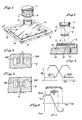
- Fig. 1 shows, in simplified perspective an optical system and stage using our alignment system. It includes a source of illumination 1, a reticle 2 with alignment slits 3, and a projection lens 5.
- the reticle carrier is not shown, but may be of any customary type.
- a neutral density filter 8 may be placed between the light source 1 and reticle 2 during alignment to reduce the exposure received by the photoresist (See Fig. 2).
- a stage 14, movable in at least X- and Y-directions is positioned below the lens. It is of the usual type (except for the detectors) and holds and carries transmissive substrate 11.
- Stage 14 includes at least one, and preferably two or three, in-stage sensors 17.
- the sensors, which are below the substrate 11, are best located remotely from one another, near corners of substrate 11, but still beneath substrate 11. For example, as shown in Fig. 1, one is near the origin, another is in the extreme X-direction from the origin, and the other is in the extreme Y-direction from the origin.
- Light source 1 controlled by adjustable shutter blades (not shown), serves to illuminate an object 3 (a pair of slits in a predetermined location on a reticle 2).
- Projection lens 5 forms an image 4 of the object upon the upper surface 6 of substrate 11. Since the substrate is transparent or translucent, an alignment sensor 17 below substrate 11 can detect the light from an image on upper surface 6.
- the substrate will have a previously-formed, partially-opaque electronic layer 9 on it and a transparent or translucent photoresist layer 7 formed upon its upper surface.
- the electronic layer 9 has alignment pairs of plate slits (plate marks) 15 in it. These plate slits 15 correspond to and complement the light image 4 from reticle slits 3 that are projected from the reticle 2 (see Figs. 3, 4, 7, and 9). Slits 15 are to be aligned with light image 4.
- each set of plate marks 15 will consist of two pairs of parallel slits orthogonal to each other; and there will be a corresponding set of reticle slits 3.
- the alignment image 4 is projected through the same lens (TTL) as the circuit image to be projected, using the same light source (actinic light) as is used to perform the exposure.
- TTL lens
- actinic light actinic light
- Alignment is achieved by moving stage 14 in X-, Y-, and ⁇ -directions as may be required. Alternatively, it may be done by adjustment of the position of the reticle. Alignment, as described below, can be achieved by moving the stage relative to the reticle by any customary means or as described in the above-mentioned patent application. The movement is controlled by electrical signals derived from the sensors.
- Transparent substrate 11 is carried by a stage 14, the stage being movable in the X-, Y-, and ⁇ -directions.
- Sensors 17 are mounted within the stage 14 in positions so as to be almost in contact with the lower surface 13 of substrate 11, about 100 microns below, and to receive a light field (image 4) through the substrate. See Figs. 2 and 8.
- the sensor is preferably sufficiently small so that it can ride within the stage rather than having to be attached to the instrument base; this eliminates stage complexity and compromise of mechanical integrity.
- the resulting lower cost is important since it permits multiple sensors to be mounted and so provide more positional information.
- Our transmission alignment system employs a relatively simple principle.
- a slit opening 3 (reticle slit) on the reticle 2 is projected onto the upper surface 6 of the transparent substrate 11, forming a slit image 4.
- the reticle slit image 4 is near the plate mark 15 (the plate slit in the electronic layer)
- some of the light will be transmitted through the plate mark 15 to the in-stage sensor 17.
- the substrate 11 is moved (by relative motion of stage 14 with respect to the slit image 4), more or less of the image light will be transmitted (see Figs. 3 and 4).
- the light transmitted will be a function of substrate (stage) position.
- a sensor 17 is underneath each overlapping set, e.g., image 4 and plate mark 15L as one set and image 4 and plate mark 15R as another set, and electrical signals are produced which correspond to the light received at each detector and also to the difference in light transmitted through the left plate mark 15L as compared to the right plate mark 15 R. These electrical signals are functionally related to the degree of alignment.
- a computer may be used to receive the electrical signals from the sensors and to use them to automatically control movement of stage 14 until alignment is achieved.
- the computer may control movement of the reticle carrier to achieve alignment.
- the plate marks 15 need not be completely transparent, nor need the photoresist background be completely opaque (though lack of opacity could raise the noise level). If the marks are partially transmitting, the sensitivity of alignment to detection noise is more important because the slope of the sensor signal in the linear range (Fig. 6) is decreased.
- the quadcell sensor 17 is shown in Figs. 8 and 9.
- Silicon detectors 18 have reasonable responses to actinic wavelength (such as 436 nm) and can be used. Also, the light power levels normally used are such that noise generated in detection and amplification contribute negligibly to positional error. Thus, commercially available silicon quadrant detectors will function satisfactorily.
- the upper and lower surfaces 6 and 13 of the substrate can cause internal reflections within the substrate and so interfere with the detection process.
- Normally, approximately 96% of the light passing through the plate mark 15 will be transmitted through the lower (back) side 13 of substrate 11 (Figs. 2 and 8).
- the remaining 4% will be reflected back within the substrate and mostly emerge following internal reflection off the top side 6 of the substrate.
- the diameter of rods 19 is large enough so that the light in the ⁇ 10° cone angle exiting a typical projection lens will be "captured” by the rods 19 even if there is some misalignment between the rods 19 and the plate marks 15. Once “captured”, the light will stay in the rod (due to total internal reflection) until it reaches the photocell 18 at the exit end of the rod.
- the detected light will be proportional to the light transmitted by the corresponding plate mark 15 and independent of the light transmitted through other plate marks. Due to the "scrambling" of the light in the rod, the detected signal will also be insensitive to positional differences between the rod and its corresponding plate mark (resulting from variations in sensitivity over the surface of the cell).
- the light channels 19 may have any desired cross-sectional configuration. However, for the best "scrambling", a polygonal cross-section, such as a triangle, square, or hexagon, is preferred to a circular one.
- the light channels 19 can be formed of hollow tubes with internally reflecting surfaces to accomplish the same result.
- the transmission of each slit in the plate marks can be different due to non-uniformity in the film deposition process. Calibration is required to insure accurate alignment. (The film may be non-uniform from one slit region to another.) This insures that the system remains linear.
Landscapes
- Physics & Mathematics (AREA)
- General Physics & Mathematics (AREA)
- Exposure Of Semiconductors, Excluding Electron Or Ion Beam Exposure (AREA)
- Exposure And Positioning Against Photoresist Photosensitive Materials (AREA)
- Liquid Crystal (AREA)
Applications Claiming Priority (2)
| Application Number | Priority Date | Filing Date | Title |
|---|---|---|---|
| US07/193,887 US4855792A (en) | 1988-05-13 | 1988-05-13 | Optical alignment system for use in photolithography and having reduced reflectance errors |
| US193887 | 1988-05-13 |
Publications (3)
| Publication Number | Publication Date |
|---|---|
| EP0341848A2 true EP0341848A2 (fr) | 1989-11-15 |
| EP0341848A3 EP0341848A3 (en) | 1990-06-13 |
| EP0341848B1 EP0341848B1 (fr) | 1995-01-25 |
Family
ID=22715425
Family Applications (1)
| Application Number | Title | Priority Date | Filing Date |
|---|---|---|---|
| EP89303972A Expired - Lifetime EP0341848B1 (fr) | 1988-05-13 | 1989-04-21 | Système d'alignement optique à usage en photolithographie avec l'erreur, causée par la réflectance, réduite |
Country Status (5)
| Country | Link |
|---|---|
| US (1) | US4855792A (fr) |
| EP (1) | EP0341848B1 (fr) |
| JP (1) | JPH0218924A (fr) |
| AT (1) | ATE117813T1 (fr) |
| DE (1) | DE68920772T2 (fr) |
Cited By (3)
| Publication number | Priority date | Publication date | Assignee | Title |
|---|---|---|---|---|
| WO2005119370A3 (fr) * | 2004-05-28 | 2006-03-16 | Azores Corp | Machine et procede de lithographie a haute vitesse |
| EP0871072B1 (fr) * | 1997-04-09 | 2007-10-17 | ASML Holding N.V. | Détecteur à ouvertures multiples pour la photolithographique |
| US9001304B2 (en) | 2008-01-16 | 2015-04-07 | Carl Zeiss Smt Gmbh | Projection exposure system for microlithography with a measurement device |
Families Citing this family (15)
| Publication number | Priority date | Publication date | Assignee | Title |
|---|---|---|---|---|
| US5168306A (en) * | 1989-04-04 | 1992-12-01 | Asahi Kogaku Kogyo Kabushiki Kaisha | Exposure apparatus |
| US5198857A (en) * | 1990-03-30 | 1993-03-30 | Ushio Denski Kabushiki Kaisha | Film exposure apparatus and method of exposure using the same |
| DE4304912C2 (de) * | 1993-02-18 | 2003-03-06 | Klaus Siebert | Verfahren und Vorrichtung zur durchgehend automatischen Chipherstellung unter Vakuum |
| EP0701383A1 (fr) * | 1994-09-08 | 1996-03-13 | Zellweger Luwa Ag | Méthode et dispositif pour la transmission de données |
| US5920378A (en) * | 1995-03-14 | 1999-07-06 | Nikon Corporation | Projection exposure apparatus |
| JP4029130B2 (ja) * | 1997-06-03 | 2008-01-09 | 株式会社ニコン | 露光装置及び露光方法 |
| US7274430B2 (en) * | 1998-02-20 | 2007-09-25 | Carl Zeiss Smt Ag | Optical arrangement and projection exposure system for microlithography with passive thermal compensation |
| US20060219947A1 (en) * | 2005-03-03 | 2006-10-05 | Asml Netherlands B.V. | Dedicated metrology stage for lithography applications |
| US8547522B2 (en) * | 2005-03-03 | 2013-10-01 | Asml Netherlands B.V. | Dedicated metrology stage for lithography applications |
| JP2006313885A (ja) * | 2005-04-04 | 2006-11-16 | Canon Inc | 露光装置 |
| US7755742B2 (en) * | 2005-10-11 | 2010-07-13 | Asml Netherlands B.V. | Lithographic apparatus with mounted sensor |
| US9291560B2 (en) | 2012-04-24 | 2016-03-22 | Seagate Technology Llc | Characterization of near field transducers |
| US9613643B2 (en) * | 2013-08-05 | 2017-04-04 | Seagate Technology Llc | Alignment of optical components |
| TWI797737B (zh) | 2017-09-29 | 2023-04-01 | 美商昂圖創新公司 | 用於在曝光裝置時減少未對準誤差的方法和設備 |
| US11687010B2 (en) | 2020-02-21 | 2023-06-27 | Onto Innovation Inc. | System and method for correcting overlay errors in a lithographic process |
Family Cites Families (17)
| Publication number | Priority date | Publication date | Assignee | Title |
|---|---|---|---|---|
| JPS529503B2 (fr) * | 1972-05-26 | 1977-03-16 | ||
| US4109158A (en) * | 1976-05-27 | 1978-08-22 | Western Electric Company, Inc. | Apparatus for positioning a pair of elements into aligned intimate contact |
| JPS602772B2 (ja) * | 1976-11-01 | 1985-01-23 | 株式会社日立製作所 | 露光装置 |
| JPS5425169A (en) * | 1977-07-27 | 1979-02-24 | Mitsubishi Electric Corp | Matching method for photo mask against semiconductor wafer |
| US4286201A (en) * | 1979-02-21 | 1981-08-25 | Amistar Corporation | Automatic part positioning system |
| JPS56111225A (en) * | 1980-02-01 | 1981-09-02 | Chiyou Lsi Gijutsu Kenkyu Kumiai | X ray exposuring device |
| US4292576A (en) * | 1980-02-29 | 1981-09-29 | The United States Of America As Represented By The Secretary Of The Air Force | Mask-slice alignment method |
| US4385238A (en) * | 1981-03-03 | 1983-05-24 | Veeco Instruments Incorporated | Reregistration system for a charged particle beam exposure system |
| DE3318980C2 (de) * | 1982-07-09 | 1986-09-18 | Perkin-Elmer Censor Anstalt, Vaduz | Vorrichtung zum Justieren beim Projektionskopieren von Masken |
| JPS6018738A (ja) * | 1983-07-11 | 1985-01-30 | Nippon Kogaku Kk <Nikon> | 投影露光装置 |
| US4629313A (en) * | 1982-10-22 | 1986-12-16 | Nippon Kogaku K.K. | Exposure apparatus |
| JPS59119204A (ja) * | 1982-12-27 | 1984-07-10 | Toshiba Corp | マ−ク位置検出方法 |
| JPS6142915A (ja) * | 1984-08-06 | 1986-03-01 | Sanyo Electric Co Ltd | X線マスク転写装置 |
| US4623608A (en) * | 1985-03-14 | 1986-11-18 | Rca Corporation | Method and apparatus for coating a selected area of the surface of an object |
| JPS62139387A (ja) * | 1985-12-13 | 1987-06-23 | 株式会社ニコン | パタ−ン描画装置 |
| JPS62229942A (ja) * | 1986-03-31 | 1987-10-08 | Univ Nagoya | 光学式位置決め装置 |
| US4769680A (en) * | 1987-10-22 | 1988-09-06 | Mrs Technology, Inc. | Apparatus and method for making large area electronic devices, such as flat panel displays and the like, using correlated, aligned dual optical systems |
-
1988
- 1988-05-13 US US07/193,887 patent/US4855792A/en not_active Expired - Lifetime
-
1989
- 1989-04-21 EP EP89303972A patent/EP0341848B1/fr not_active Expired - Lifetime
- 1989-04-21 DE DE68920772T patent/DE68920772T2/de not_active Expired - Fee Related
- 1989-04-21 AT AT89303972T patent/ATE117813T1/de not_active IP Right Cessation
- 1989-05-12 JP JP1120208A patent/JPH0218924A/ja active Pending
Cited By (5)
| Publication number | Priority date | Publication date | Assignee | Title |
|---|---|---|---|---|
| EP0871072B1 (fr) * | 1997-04-09 | 2007-10-17 | ASML Holding N.V. | Détecteur à ouvertures multiples pour la photolithographique |
| WO2005119370A3 (fr) * | 2004-05-28 | 2006-03-16 | Azores Corp | Machine et procede de lithographie a haute vitesse |
| US9001304B2 (en) | 2008-01-16 | 2015-04-07 | Carl Zeiss Smt Gmbh | Projection exposure system for microlithography with a measurement device |
| US9696639B2 (en) | 2008-01-16 | 2017-07-04 | Carl Zeiss Smt Gmbh | Projection exposure system for microlithography with a measurement device |
| US10042271B2 (en) | 2008-01-16 | 2018-08-07 | Carl Zeiss Smt Gmbh | Projection exposure system for microlithography with a measurement device |
Also Published As
| Publication number | Publication date |
|---|---|
| JPH0218924A (ja) | 1990-01-23 |
| DE68920772T2 (de) | 1995-07-27 |
| US4855792A (en) | 1989-08-08 |
| ATE117813T1 (de) | 1995-02-15 |
| EP0341848A3 (en) | 1990-06-13 |
| EP0341848B1 (fr) | 1995-01-25 |
| DE68920772D1 (de) | 1995-03-09 |
Similar Documents
| Publication | Publication Date | Title |
|---|---|---|
| US4855792A (en) | Optical alignment system for use in photolithography and having reduced reflectance errors | |
| US4595295A (en) | Alignment system for lithographic proximity printing | |
| US5510892A (en) | Inclination detecting apparatus and method | |
| KR100471524B1 (ko) | 노광방법 | |
| KR20030071637A (ko) | 캘리브레이션방법, 캘리브레이션기판, 리소그래피장치 및디바이스제조방법 | |
| US6975384B2 (en) | Exposure apparatus and method | |
| KR20000065214A (ko) | 오프축 얼라인먼트 유니트를 갖는 리소그래픽 투영 장치 | |
| JPH0766904B2 (ja) | デバイス製作方法 | |
| US5912726A (en) | Projection exposure apparatus and method having a positional deviation detection system that employs light from an exposure illumination system | |
| US5572325A (en) | Apparatus for optically detecting a position of mark | |
| KR100287504B1 (ko) | 면위치검출장치를 구비한 주사노광장치 | |
| US5978069A (en) | Exposure apparatus and methods | |
| US7106419B2 (en) | Exposure method and apparatus | |
| US5929529A (en) | Reticle semiconductor wafer, and semiconductor chip | |
| JP3203676B2 (ja) | 投影露光装置 | |
| KR100239623B1 (ko) | 투영노광장치, 투영노광방법 및 반도체디바이스 제조방법 | |
| JPH09101116A (ja) | 自動焦点合わせ方法及びその装置並びにパターン検出方法及びその装置 | |
| US4007988A (en) | Manufacture of multi-layer structures | |
| JPH04348019A (ja) | 焦点位置検出装置及び投影露光装置 | |
| WO1998006009A1 (fr) | Systeme de lithographie a tele-alignement par multidetecteur | |
| EP0083710B1 (fr) | Système d'alignement pour lithographie à proximité | |
| USH1463H (en) | Method for detecting positions of photomask and substrate | |
| JPH01228130A (ja) | 投影露光方法およびその装置 | |
| US4050817A (en) | Manufacture of multi-layer structures | |
| JPH0430735B2 (fr) |
Legal Events
| Date | Code | Title | Description |
|---|---|---|---|
| PUAI | Public reference made under article 153(3) epc to a published international application that has entered the european phase |
Free format text: ORIGINAL CODE: 0009012 |
|
| AK | Designated contracting states |
Kind code of ref document: A2 Designated state(s): AT BE CH DE ES FR GB IT LI NL SE |
|
| PUAL | Search report despatched |
Free format text: ORIGINAL CODE: 0009013 |
|
| AK | Designated contracting states |
Kind code of ref document: A3 Designated state(s): AT BE CH DE ES FR GB IT LI NL SE |
|
| 17P | Request for examination filed |
Effective date: 19901029 |
|
| 17Q | First examination report despatched |
Effective date: 19930405 |
|
| GRAA | (expected) grant |
Free format text: ORIGINAL CODE: 0009210 |
|
| AK | Designated contracting states |
Kind code of ref document: B1 Designated state(s): AT BE CH DE ES FR GB IT LI NL SE |
|
| PG25 | Lapsed in a contracting state [announced via postgrant information from national office to epo] |
Ref country code: IT Free format text: LAPSE BECAUSE OF FAILURE TO SUBMIT A TRANSLATION OF THE DESCRIPTION OR TO PAY THE FEE WITHIN THE PRE;WARNING: LAPSES OF ITALIAN PATENTS WITH EFFECTIVE DATE BEFORE 2007 MAY HAVE OCCURRED AT ANY TIME BEFORE 2007. THE CORRECT EFFECTIVE DATE MAY BE DIFFERENT FROM THE ONE RECORDED.SCRIBED TIME-LIMIT Effective date: 19950125 Ref country code: ES Free format text: THE PATENT HAS BEEN ANNULLED BY A DECISION OF A NATIONAL AUTHORITY Effective date: 19950125 Ref country code: AT Effective date: 19950125 Ref country code: BE Effective date: 19950125 |
|
| REF | Corresponds to: |
Ref document number: 117813 Country of ref document: AT Date of ref document: 19950215 Kind code of ref document: T |
|
| REF | Corresponds to: |
Ref document number: 68920772 Country of ref document: DE Date of ref document: 19950309 |
|
| ET | Fr: translation filed | ||
| PG25 | Lapsed in a contracting state [announced via postgrant information from national office to epo] |
Ref country code: SE Effective date: 19950425 |
|
| PLBE | No opposition filed within time limit |
Free format text: ORIGINAL CODE: 0009261 |
|
| STAA | Information on the status of an ep patent application or granted ep patent |
Free format text: STATUS: NO OPPOSITION FILED WITHIN TIME LIMIT |
|
| 26N | No opposition filed | ||
| PGFP | Annual fee paid to national office [announced via postgrant information from national office to epo] |
Ref country code: GB Payment date: 19960415 Year of fee payment: 8 |
|
| PGFP | Annual fee paid to national office [announced via postgrant information from national office to epo] |
Ref country code: FR Payment date: 19960423 Year of fee payment: 8 |
|
| PGFP | Annual fee paid to national office [announced via postgrant information from national office to epo] |
Ref country code: DE Payment date: 19960430 Year of fee payment: 8 Ref country code: NL Payment date: 19960430 Year of fee payment: 8 |
|
| PGFP | Annual fee paid to national office [announced via postgrant information from national office to epo] |
Ref country code: CH Payment date: 19960506 Year of fee payment: 8 |
|
| PG25 | Lapsed in a contracting state [announced via postgrant information from national office to epo] |
Ref country code: GB Effective date: 19970421 |
|
| PG25 | Lapsed in a contracting state [announced via postgrant information from national office to epo] |
Ref country code: CH Free format text: LAPSE BECAUSE OF NON-PAYMENT OF DUE FEES Effective date: 19970430 Ref country code: LI Free format text: LAPSE BECAUSE OF NON-PAYMENT OF DUE FEES Effective date: 19970430 |
|
| PG25 | Lapsed in a contracting state [announced via postgrant information from national office to epo] |
Ref country code: NL Effective date: 19971101 |
|
| GBPC | Gb: european patent ceased through non-payment of renewal fee |
Effective date: 19970421 |
|
| REG | Reference to a national code |
Ref country code: CH Ref legal event code: PL |
|
| PG25 | Lapsed in a contracting state [announced via postgrant information from national office to epo] |
Ref country code: FR Free format text: LAPSE BECAUSE OF NON-PAYMENT OF DUE FEES Effective date: 19971231 |
|
| PG25 | Lapsed in a contracting state [announced via postgrant information from national office to epo] |
Ref country code: DE Free format text: LAPSE BECAUSE OF NON-PAYMENT OF DUE FEES Effective date: 19980101 |
|
| NLV4 | Nl: lapsed or anulled due to non-payment of the annual fee |
Effective date: 19971101 |
|
| REG | Reference to a national code |
Ref country code: FR Ref legal event code: ST |