EP0341531A2 - Amplificateur à large bande réglable - Google Patents
Amplificateur à large bande réglable Download PDFInfo
- Publication number
- EP0341531A2 EP0341531A2 EP89107859A EP89107859A EP0341531A2 EP 0341531 A2 EP0341531 A2 EP 0341531A2 EP 89107859 A EP89107859 A EP 89107859A EP 89107859 A EP89107859 A EP 89107859A EP 0341531 A2 EP0341531 A2 EP 0341531A2
- Authority
- EP
- European Patent Office
- Prior art keywords
- amplifier
- output
- differential amplifier
- reference voltage
- differential
- Prior art date
- Legal status (The legal status is an assumption and is not a legal conclusion. Google has not performed a legal analysis and makes no representation as to the accuracy of the status listed.)
- Withdrawn
Links
Images


Classifications
-
- H—ELECTRICITY
- H03—ELECTRONIC CIRCUITRY
- H03G—CONTROL OF AMPLIFICATION
- H03G1/00—Details of arrangements for controlling amplification
- H03G1/0005—Circuits characterised by the type of controlling devices operated by a controlling current or voltage signal
- H03G1/0017—Circuits characterised by the type of controlling devices operated by a controlling current or voltage signal the device being at least one of the amplifying solid-state elements
- H03G1/0023—Circuits characterised by the type of controlling devices operated by a controlling current or voltage signal the device being at least one of the amplifying solid-state elements in emitter-coupled or cascode amplifiers
-
- H—ELECTRICITY
- H03—ELECTRONIC CIRCUITRY
- H03D—DEMODULATION OR TRANSFERENCE OF MODULATION FROM ONE CARRIER TO ANOTHER
- H03D7/00—Transference of modulation from one carrier to another, e.g. frequency-changing
- H03D7/14—Balanced arrangements
- H03D7/1425—Balanced arrangements with transistors
- H03D7/1433—Balanced arrangements with transistors using bipolar transistors
-
- H—ELECTRICITY
- H03—ELECTRONIC CIRCUITRY
- H03D—DEMODULATION OR TRANSFERENCE OF MODULATION FROM ONE CARRIER TO ANOTHER
- H03D7/00—Transference of modulation from one carrier to another, e.g. frequency-changing
- H03D7/14—Balanced arrangements
- H03D7/1425—Balanced arrangements with transistors
- H03D7/1458—Double balanced arrangements, i.e. where both input signals are differential
-
- H—ELECTRICITY
- H03—ELECTRONIC CIRCUITRY
- H03D—DEMODULATION OR TRANSFERENCE OF MODULATION FROM ONE CARRIER TO ANOTHER
- H03D7/00—Transference of modulation from one carrier to another, e.g. frequency-changing
- H03D7/14—Balanced arrangements
- H03D7/1425—Balanced arrangements with transistors
- H03D7/1491—Arrangements to linearise a transconductance stage of a mixer arrangement
-
- H—ELECTRICITY
- H03—ELECTRONIC CIRCUITRY
- H03D—DEMODULATION OR TRANSFERENCE OF MODULATION FROM ONE CARRIER TO ANOTHER
- H03D7/00—Transference of modulation from one carrier to another, e.g. frequency-changing
- H03D7/16—Multiple-frequency-changing
- H03D7/165—Multiple-frequency-changing at least two frequency changers being located in different paths, e.g. in two paths with carriers in quadrature
-
- H—ELECTRICITY
- H03—ELECTRONIC CIRCUITRY
- H03D—DEMODULATION OR TRANSFERENCE OF MODULATION FROM ONE CARRIER TO ANOTHER
- H03D2200/00—Indexing scheme relating to details of demodulation or transference of modulation from one carrier to another covered by H03D
- H03D2200/0001—Circuit elements of demodulators
- H03D2200/0019—Gilbert multipliers
-
- H—ELECTRICITY
- H03—ELECTRONIC CIRCUITRY
- H03D—DEMODULATION OR TRANSFERENCE OF MODULATION FROM ONE CARRIER TO ANOTHER
- H03D2200/00—Indexing scheme relating to details of demodulation or transference of modulation from one carrier to another covered by H03D
- H03D2200/0001—Circuit elements of demodulators
- H03D2200/0033—Current mirrors
-
- H—ELECTRICITY
- H03—ELECTRONIC CIRCUITRY
- H03D—DEMODULATION OR TRANSFERENCE OF MODULATION FROM ONE CARRIER TO ANOTHER
- H03D2200/00—Indexing scheme relating to details of demodulation or transference of modulation from one carrier to another covered by H03D
- H03D2200/0041—Functional aspects of demodulators
- H03D2200/0082—Quadrature arrangements
-
- H—ELECTRICITY
- H03—ELECTRONIC CIRCUITRY
- H03D—DEMODULATION OR TRANSFERENCE OF MODULATION FROM ONE CARRIER TO ANOTHER
- H03D7/00—Transference of modulation from one carrier to another, e.g. frequency-changing
- H03D7/18—Modifications of frequency-changers for eliminating image frequencies
Definitions
- the invention relates to a controllable broadband amplifier according to the preamble of claim 1.
- Such a broadband amplifier is known for example from Electronics Letters, Vol. 22, No. 8 (1986) pp. 415-516.
- the fourth differential amplifier reduces the DC voltage fluctuations occurring at the amplifier output when the gain is controlled.
- a DC voltage fluctuation remains at the output of around 12mV a control range of 20dB.
- the present invention is therefore based on the object of specifying a controllable broadband amplifier of the type mentioned in the preamble of patent claim 1, which has improved stability of the DC voltage level at the amplifier output over a large control range.
- the invention is described in claim 1.
- the subclaims contain advantageous designs and developments of the invention.
- measures are specified with which noise contributions occurring during stabilization can be largely suppressed without impairing the cutoff frequency of the amplifier.
- the broadband amplifier according to the invention can be used particularly advantageously as transadmittance, i.e. as a voltage / current converter in a mixer arrangement cascaded from transadmittance and mixer stage using differential amplifiers in the mixer stage, the output currents of the broadband amplifier forming the operating currents of the differential amplifiers of the mixer stage.
- the mixing stage is preferably designed as a quadrature mixing stage with two orthogonally controlled four-quadrant multipliers.
- Such a mixer arrangement is characterized above all by low current consumption, low noise, high linearity independent of the control voltage, large control dynamic range and good reverse insulation.
- the two inputs E11 and E12 of the differential amplifier D1 are connected to the two useful signal inputs E1 and E2.
- the reference voltage electrode B1 of the differential amplifier D1 is via a Constant current source I1 connected to one pole K1 of the operating voltage.
- the output A11 is connected to the reference voltage electrode B2 of the differential amplifier D2 and the other output A12 is connected to the reference voltage electrode B3 of the differential amplifier D3.
- the inputs of the differential amplifiers D2 and D3 are connected in parallel and are each connected to an input ER1 or ER2, which are provided for supplying the control voltage.
- An output A22 of the differential amplifier D2 is connected to an output A32 of the differential amplifier D3 and connected to the reference voltage electrode B4 of a differential amplifier D4.
- the respective other output A21 or A31 of the differential amplifier D2 and D3 is connected to an output A41 or A42 of the differential amplifier and to a respective connection point P1 or P2.
- the connection points P1 and P2 are connected to the pole K2 of the operating voltage and to at least one output A1 and A2 of the broadband amplifier via a resistor R2 and R3, respectively.
- the resistors R2, R3 serve as transimpedance for decoupling the signal.
- Other transimpedances, a cascode arrangement, a coupling-out current mirror or the like can also be used for signal coupling in a manner known per se.
- two series-connected resistors R41 and R42 with the same resistance value are provided, which are connected between the non-interconnected outputs A21, A31.
- the connection point Q of the resistors R41 and R42 is with connected to the two inputs E41 and E42 of the differential amplifier D3.
- the resistors R41 and R42 have a high resistance to the resistors R2 and R3 and therefore have practically no influence on the amplification of the broadband amplifier.
- the current source I1 which is connected between the reference voltage electrode B1 of the differential amplifier D1 and the pole K1 of the operating voltage, ensures a constant current consumption Jo of the broadband amplifier. It consists e.g. from a transistor with negative feedback in its emitter lead in an emitter circuit.
- the current source can also be realized by a current mirror circuit known per se, so that the voltage drop at the current source can be kept very low.
- the broadband amplifier When the broadband amplifier is driven at its control voltage inputs ER1 and ER2, for example the current at outputs A21 and A31 of differential amplifiers D2 and D3 is increased and the current at outputs A22 and A32 is decreased.
- the total current at the reference voltage electrode B4 of the differential amplifier D4 is only dependent on the control voltage, but not on the input signal.
- the differential amplifier D4 divides the total current into two equal parts and feeds them to the two outputs A1 and A2 of the broadband amplifier.
- An input signal at the input terminals E1, E2 modulates the operating currents of the differential amplifiers D2 and D3 in phase.
- the currents at outputs A21 and A31 are lower than the operating currents by a factor set by the control voltage.
- the partial currents fed back via the differential amplifier D4 are not modulated by the input signal and therefore only influence the DC component in the output currents JA1, JA2 of the amplifier or, via the transimpedances at the output, the DC voltage level of the output voltages at A1, A2. If the control voltage changes, only the AC voltage component at the outputs is changed, while the DC voltage component remains constant. The fluctuation of the DC voltage level at the output can easily be kept below 1 mV over a control dynamic range of 50 dB.
- FIG. 2 is a detailed circuit diagram of the one shown in FIG. 1 shown as a block diagram differential amplifier.
- the reference symbols refer to the differential amplifier D1.
- the differential amplifiers each contain two transistors, e.g. T11 and T12, whose base connections form the two inputs E11 and E12, whose collector connections form the two outputs A11 and A12 and whose interconnected emitters form the reference voltage electrode B1.
- the differential amplifiers D2 to D4 are constructed and connected in the same way.
- the reference numerals and their indices are chosen so that the assignment of the connections to the transistor electrodes is easily recognizable.
- controllable broadband amplifier provides that a resistor R11 or R12 is interposed in the emitter lead of the transistors T11 and T12.
- the broadband amplifier described here combines the properties of large signal strength and DC-stabilized outputs almost independently of the control position with high control dynamics and low noise contribution.
- the emitters of the two transistors T11, T12 of the input stage D1 can each be connected to a reference potential via a separate current source and to one another via a negative feedback resistor. By varying this negative feedback resistance, the effective negative feedback and thus linearity and noise can be influenced without the operating points of the transistors shifting.
- the differential amplifier D4 divides the current through B4 symmetrically and therefore provides a maximum noise contribution, which according to FIG. 1 acts directly on the outputs A1, A2.
- An advantageous development of the invention therefore provides measures for suppressing these noise components.
- FIG. 3 shows the resistors R41 and R42 in two resistors R411 and R412 and R421 and R422 divided, the respective connection point VP1 or VP2 connected to ground potential through a capacitor C41 or C42 and the outputs A41 and A42 of the differential amplifier D4 connected to the respective connection points, i.e. output A41 with connection point VP1 and output A42 with the connection point VP2.
- resistors R412, R322 it is also advantageously possible to use inductors for decoupling the noise suppression capacitors from the outputs, which isolate the outputs for the useful signal frequency with high impedance from the capacitors, but which do not cause a voltage drop for the quiescent current components flowing via D4.
- the capacitors are advantageously integrated in the circuit arrangement and dimensioned such that the limit frequency defined by C41 or C42 and on the transistors of D4 effective output impedances is clearly and the useful signal frequency.
- the capacitors C41, C42 can be replaced without disadvantage by a capacitor connected between the points VP1 and VP2.
- the controllable broadband amplifier according to the invention can be used particularly advantageously in a cascaded mixer arrangement as a voltage-current converter (transadmittance) for an input signal in such a way that the output currents of the amplifier form the operating currents of a mixer stage.
- the cascading of a transadmittance with a mixing stage is known per se and is described, for example, in IEEE Journal of Solid-State Circuits, Vo. SC-3, No. 4, Dec. 1968, pp. 365-373.
- Particularly advantageous arrangements have several separate mixers in the mixing stage, for example for the quadrature mixing of a single input signal with two orthogonal superposition signals.
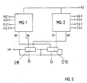
- FIG. 4 shows a mixer stage with two four-quadrant multipliers as mixers MQ1, MQ2, each of which contains a transistor quartet.
- the transistor quartets are each combined into two differential amplifiers connected in parallel on the input side and cross-connected on the output side.
- the inputs of the differential amplifiers connected in parallel are connected to the inputs EQ1 and EQ2 of the multiplier quartet.
- the cross-connected outputs of the differential amplifiers are connected to the outputs AQ1 and AQ2 of the multiplier quartet and are also connected to the pole K2 of the operating circuit via a resistor R5 or R6.
- a transimpedance instead of the resistors R5 or R6, a transimpedance, a coupling-out current mirror or a resonant load can be provided.
- the reference voltage electrode B5 is connected to the output A2 of the broadband amplifier (FIG. 1) and the reference voltage electrode B6 to the output A1 of the broadband amplifier. (The resistors R2 and R3 in FIG. 1 are omitted).
- decoupling resistors R21 and R22 or R31 and R32 are advantageous for improving the current distribution. All resistors R21, R22, R31 and R32 have the same resistance value.
- a further improvement in the equality of the current distribution between the common voltage-current conversion stage on the one hand and the two multiplier quartets on the other hand allows the division via differential amplifiers D9 and D10 (FIG. 5).
- the inputs of the differential amplifiers D9 and D10 are connected to an auxiliary voltage UH which is common to all connections and to which no special requirements have to be made due to the high-resistance feed-in by the broadband amplifier.
- auxiliary voltage UH which is common to all connections and to which no special requirements have to be made due to the high-resistance feed-in by the broadband amplifier.
- the in FIG. Mixers 4 and 5 outlined are also known as Gilbert mixers or double-balanced mixers and have the particular advantage that the oscillator frequency in the mixer output signals at AQ1, AQ2 and AQ3, AQ4 is already largely suppressed.
- the other's reference voltage electrode B12 Differential amplifier D12 is connected to the other output A2 of the broadband amplifier and is located at the inputs E121, E122 to an orthogonal LO, that is 90 ° phase shifted oscillator signal LOQ to.
- the differential amplifiers D5 to D8 or D11, D12 preferably operate in switching mode, i.e. with square-wave control signals and then only provide a negligible noise contribution compared to the other components.
- FIG. 7 schematically sketched again with subdivision into successive circuit stages, stating current distribution ratios and interference contributions in the individual stages.
- the noise contribution N1 of the input stage represents the main noise component of the entire arrangement, so that the execution of the input stage is of crucial importance.
- the demands for low noise contribution, high linearity and low power consumption lead to contradicting tendencies when defining individual parameters. For example, the linearity properties are improved by high emitter negative feedback resistances, but the noise properties are worsened. A high quiescent current also favors the linearity properties, but is disadvantageous in terms of power consumption.
- the dimensioning in detail must therefore be based on the requirements of the individual case.
- the useful signal components are only contained in push-pull in the currents J21 and J31 with an amplitude weakened compared to J11, J12.
- the noise contribution of the differential amplifier D4 can be reduced by increasing the transistor areas and the lower path resistances of the transistors that can be achieved thereby. However, this also leads to higher transistor capacitances in the differential amplifier stage D4 and this in turn results in a lower boundary frequency of the arrangement.
- the even one Distribution can be done both via resistors as in FIG. 4 and via differential amplifiers as in FIG. 5 take place, the version with differential amplifiers having a better isolation of the mixer, but also a higher noise contribution NV.
- It is important that the signal-to-quiescent current ratio is not changed in the division in the distribution stage, since all current components are reduced in the same ratio and thus the signal-to-quiescent current ratio in the mixer output signals is determined by the input stage and the control stage. In particular, the sum of the currents through both mixer quartets MQ1, MQ2 is available as a quiescent current in the input stage.
- the interference contributions NM of the mixers are heavily dependent on their operating state.
- the interference components essentially comprising noise and intermodulation distortions by the mixer are small overall and depend on the slope of the square-wave signals. Noteworthy interference contributions arise primarily at the switchover times. In the case of linear operation of the mixers, the interference components are higher and can no longer be neglected.
- the principle of cascading a transadmittance input amplifier that converts an input voltage into an output current with several mixers connected in parallel can also be used for amplifiers with only one current output.
- the advantage that linearity and noise behavior are essentially determined by the input stage and not significantly affected by the division This also applies in this case and, by requiring only one input stage for several mixer stages, in particular enables the input stage to be operated with a relatively higher quiescent current with an overall acceptable power consumption of the cascaded arrangement.
- the mixer quartets MQ1, MQ2 with push-pull control via A1, A2 simple push-pull mixer stages with only one differential amplifier each occur, for example.
Landscapes
- Engineering & Computer Science (AREA)
- Power Engineering (AREA)
- Amplifiers (AREA)
- Control Of Amplification And Gain Control (AREA)
Applications Claiming Priority (2)
| Application Number | Priority Date | Filing Date | Title |
|---|---|---|---|
| DE3816075 | 1988-05-11 | ||
| DE3816075 | 1988-05-11 |
Publications (2)
| Publication Number | Publication Date |
|---|---|
| EP0341531A2 true EP0341531A2 (fr) | 1989-11-15 |
| EP0341531A3 EP0341531A3 (fr) | 1991-05-15 |
Family
ID=6354144
Family Applications (1)
| Application Number | Title | Priority Date | Filing Date |
|---|---|---|---|
| EP19890107859 Withdrawn EP0341531A3 (fr) | 1988-05-11 | 1989-04-29 | Amplificateur à large bande réglable |
Country Status (4)
| Country | Link |
|---|---|
| US (1) | US4931746A (fr) |
| EP (1) | EP0341531A3 (fr) |
| JP (1) | JPH01320807A (fr) |
| DE (1) | DE3915418C2 (fr) |
Families Citing this family (24)
| Publication number | Priority date | Publication date | Assignee | Title |
|---|---|---|---|---|
| JPH0417405A (ja) * | 1990-05-10 | 1992-01-22 | Alps Electric Co Ltd | ミキサ回路 |
| DE4130705C2 (de) * | 1990-09-19 | 1996-07-11 | Telefunken Microelectron | Schaltungsanordnung zur Frequenzumsetzung |
| WO1993015560A1 (fr) * | 1992-02-03 | 1993-08-05 | Motorola, Inc. | Circuit melangeur equilibre |
| DE4206164C2 (de) * | 1992-02-28 | 1994-12-08 | Telefunken Microelectron | HF-Mischstufe in Basisschaltung |
| FR2695272B1 (fr) * | 1992-08-26 | 1994-12-09 | Philips Composants | Circuit mélangeur pour des signaux de radio ou de télévision. |
| US5491447A (en) * | 1994-05-13 | 1996-02-13 | International Business Machines Corporation | Operational transconductance amplifier with independent transconductance and common mode feedback control |
| JPH0969730A (ja) * | 1995-08-30 | 1997-03-11 | Nec Corp | 周波数ミキサ回路 |
| US5805988A (en) * | 1995-12-22 | 1998-09-08 | Microtune, Inc. | System and method for switching an RF signal between mixers |
| US6147543A (en) * | 1996-01-19 | 2000-11-14 | Motorola, Inc. | Method and apparatus for selecting from multiple mixers |
| US5884154A (en) * | 1996-06-26 | 1999-03-16 | Raytheon Company | Low noise mixer circuit having passive inductor elements |
| US5933771A (en) * | 1997-06-20 | 1999-08-03 | Nortel Networks Corporation | Low voltage gain controlled mixer |
| DE69822836T2 (de) | 1998-10-30 | 2005-03-24 | Stmicroelectronics S.R.L., Agrate Brianza | I-Q Mischer mit niedrigem Rauschen |
| US6570427B2 (en) * | 2000-12-21 | 2003-05-27 | Intersil Americas Inc. | Variable transconductance amplifier |
| KR100530740B1 (ko) * | 2001-08-11 | 2005-11-28 | 한국전자통신연구원 | 주파수-종속 부성 저항기 |
| CA2404721C (fr) * | 2001-10-12 | 2005-06-07 | Research In Motion Limited | Oscillateur a melangeur integre |
| US7054609B2 (en) * | 2002-04-04 | 2006-05-30 | Telefonaktiebolaget Lm Ericsson (Publ) | Linearity improvement of Gilbert mixers |
| US7062247B2 (en) * | 2002-05-15 | 2006-06-13 | Nec Corporation | Active double-balanced mixer |
| DE10222622A1 (de) * | 2002-05-17 | 2003-11-27 | Marconi Comm Gmbh | Aufwärts-Frequenzumsetzer |
| JP2004180281A (ja) * | 2002-11-13 | 2004-06-24 | Renesas Technology Corp | 直交ミキサ回路及びそれを用いた携帯端末 |
| KR100574470B1 (ko) * | 2004-06-21 | 2006-04-27 | 삼성전자주식회사 | 전류증폭결합기를 포함하는 선형 혼합기회로 |
| KR100645531B1 (ko) * | 2005-11-10 | 2006-11-14 | 삼성전자주식회사 | 저전력을 위한 고속 모드 스위칭 주파수 합성 장치 및 방법 |
| DE102006043902B4 (de) * | 2006-09-19 | 2016-09-22 | Intel Deutschland Gmbh | Stromwandler, Frequenzmischer und Verfahren zur Frequenzmischung |
| WO2008069478A1 (fr) * | 2006-12-05 | 2008-06-12 | Electronics And Telecommunications Research Institute | Amplificateur de limitation ayant des caractéristiques de gain et de bande passante améliorées |
| US8089309B2 (en) * | 2009-06-26 | 2012-01-03 | Bae Systems Information And Electronic Systems Integration Inc. | Transimpedance amplifier input stage mixer |
Family Cites Families (7)
| Publication number | Priority date | Publication date | Assignee | Title |
|---|---|---|---|---|
| GB1160603A (en) * | 1967-07-19 | 1969-08-06 | Marconi Co Ltd | Improvements in or relating to Transistorised Modulatable Oscillation Generators, Demodulators, Phase Detectors and Frequency Shifters |
| US3550040A (en) * | 1968-05-31 | 1970-12-22 | Monsanto Co | Double-balanced modulator circuit readily adaptable to integrated circuit fabrication |
| JPS5519444B2 (fr) * | 1972-12-29 | 1980-05-26 | ||
| SU450307A1 (ru) * | 1973-07-12 | 1974-11-15 | Предприятие П/Я Х-5885 | Балансный пребразователь частоты |
| JPS6119208A (ja) * | 1984-07-05 | 1986-01-28 | Murata Mfg Co Ltd | 密封型電子部品の製造方法及びそれに使用される多連ケ−ス部材 |
| US4766400A (en) * | 1986-12-19 | 1988-08-23 | Kabushiki Kaisha Toshiba | Variable-transconductance four-quadrant Gilbert-type modulator with feedback circuitry in improved NMR transmission |
| DE3732171A1 (de) * | 1987-09-24 | 1989-04-06 | Adolf Strobel Gmbh & Co Kg | Mischschaltung zur erzeugung eines modulationsprodukts |
-
1989
- 1989-04-29 EP EP19890107859 patent/EP0341531A3/fr not_active Withdrawn
- 1989-05-09 US US07/352,546 patent/US4931746A/en not_active Expired - Fee Related
- 1989-05-11 DE DE3915418A patent/DE3915418C2/de not_active Expired - Lifetime
- 1989-05-11 JP JP1116240A patent/JPH01320807A/ja active Pending
Non-Patent Citations (2)
| Title |
|---|
| ELECTRONICS LETTERS, Band 22, Nr. 8, 10. April 1986, Seiten 415-416, London, GB; T. KINOSHITA et al.: "New monolithic AGC amplifier stabilising output DC level for 560 Mbit/s optical transmission" * |
| IEEE JOURNAL OF SOLID-STATE CIRCUITS, Band SC-21, Nr. 4, August 1986, Seiten 534-537, New York, US; R.G. MEYER: "Intermodulation in high-frequency bipolar transistor integrated-circuit mixers" * |
Also Published As
| Publication number | Publication date |
|---|---|
| EP0341531A3 (fr) | 1991-05-15 |
| DE3915418C2 (de) | 1999-02-11 |
| DE3915418A1 (de) | 1989-11-16 |
| JPH01320807A (ja) | 1989-12-26 |
| US4931746A (en) | 1990-06-05 |
Similar Documents
| Publication | Publication Date | Title |
|---|---|---|
| EP0341531A2 (fr) | Amplificateur à large bande réglable | |
| DE69706953T2 (de) | Mischer mit Unterdrückung der Spiegelfrequenz | |
| DE69426650T2 (de) | Mischer für Sender, mit einem Eingang im Strom-Modus | |
| DE69207612T2 (de) | Frequenzkompensierter Mehrstufenverstärker mit verschachtelter kapazitiver Neutralisierung und innerer Mehrweg-Vorwärtssteuerung | |
| DE69009773T2 (de) | Voll differentieller cmos-leistungsverstärker. | |
| DE3879391T2 (de) | Symmetrischer spannungs/strom-wandler und damit versehene doppelsymmetrische mischschaltung. | |
| DE69321902T2 (de) | Umsetzerschaltung und Doppelgegentaktmischer | |
| DE69422010T2 (de) | Phasenschiebverstärker und seine Verwendung in einer Zusammenführungsschaltung | |
| DE2513906B2 (de) | Stromspiegelverstaerker | |
| DE1901804B2 (de) | Stabilisierter differentialverstaerker | |
| EP0073929A2 (fr) | Circuit semi-conducteur de traitement de signaux réalisable en circuit intégré | |
| EP1067673A2 (fr) | Mélangeur avec linéarité améliorée | |
| EP1405413A2 (fr) | Circuit multiplicateur | |
| DE69315553T2 (de) | Differenzverstärkeranordnung | |
| DE10344876B3 (de) | Signalverarbeitungseinrichtung, insbesondere für den Mobilfunk | |
| EP1119903B1 (fr) | Circuiterie pour melanger un signal d'entree et un signal d'oscillateur | |
| DE69611967T2 (de) | Gefaltetes aktives Filter | |
| EP0077500A2 (fr) | Diviseur de fréquence intégrable | |
| DE102004030039B3 (de) | Mischerschaltung | |
| DE69707592T2 (de) | Ein mikrowellen spannungsgesteuerter Oszillator mit verminderter Versorgungsspannung | |
| EP0133618B1 (fr) | Circuit oscillateur haute fréquence à quartz sous forme de circuit intégré monolithique | |
| WO2003005561A2 (fr) | Circuit interface destine a etre connecte a une sortie d'un convertisseur de frequence | |
| DE3032660C2 (de) | Demodulatorschaltung zum Demodulieren eines winkelmodulierten Eingangssignals | |
| DE3007715A1 (de) | Verstaerkerschaltung mit durch eine steuerspannung steuerbarer gesamtverstaerkung | |
| DE1903913B2 (de) | Breitband-verstaerkerschaltung |
Legal Events
| Date | Code | Title | Description |
|---|---|---|---|
| PUAI | Public reference made under article 153(3) epc to a published international application that has entered the european phase |
Free format text: ORIGINAL CODE: 0009012 |
|
| AK | Designated contracting states |
Kind code of ref document: A2 Designated state(s): AT BE CH DE ES FR GB GR IT LI LU NL SE |
|
| PUAL | Search report despatched |
Free format text: ORIGINAL CODE: 0009013 |
|
| AK | Designated contracting states |
Kind code of ref document: A3 Designated state(s): AT BE CH DE ES FR GB GR IT LI LU NL SE |
|
| 17P | Request for examination filed |
Effective date: 19910716 |
|
| STAA | Information on the status of an ep patent application or granted ep patent |
Free format text: STATUS: THE APPLICATION HAS BEEN WITHDRAWN |
|
| 18W | Application withdrawn |
Withdrawal date: 19920605 |
|
| R18W | Application withdrawn (corrected) |
Effective date: 19920605 |