EP0341221A2 - Bipolarer Leistungshalbleiteranordnung und Verfahren zur ihrer Herstellung - Google Patents
Bipolarer Leistungshalbleiteranordnung und Verfahren zur ihrer Herstellung Download PDFInfo
- Publication number
- EP0341221A2 EP0341221A2 EP89830186A EP89830186A EP0341221A2 EP 0341221 A2 EP0341221 A2 EP 0341221A2 EP 89830186 A EP89830186 A EP 89830186A EP 89830186 A EP89830186 A EP 89830186A EP 0341221 A2 EP0341221 A2 EP 0341221A2
- Authority
- EP
- European Patent Office
- Prior art keywords
- emitter
- base
- layer
- metal
- regions
- Prior art date
- Legal status (The legal status is an assumption and is not a legal conclusion. Google has not performed a legal analysis and makes no representation as to the accuracy of the status listed.)
- Granted
Links
- 239000004065 semiconductor Substances 0.000 title claims abstract description 11
- 238000000034 method Methods 0.000 title claims description 26
- 238000004519 manufacturing process Methods 0.000 title claims description 8
- 239000002184 metal Substances 0.000 claims abstract description 55
- 229910052751 metal Inorganic materials 0.000 claims abstract description 55
- 239000004642 Polyimide Substances 0.000 claims abstract description 18
- 229920001721 polyimide Polymers 0.000 claims abstract description 18
- 239000011159 matrix material Substances 0.000 claims abstract description 13
- 238000001465 metallisation Methods 0.000 claims description 26
- 238000000151 deposition Methods 0.000 claims description 15
- 230000007717 exclusion Effects 0.000 claims description 8
- 230000001413 cellular effect Effects 0.000 claims description 7
- 230000008021 deposition Effects 0.000 claims description 7
- 230000015572 biosynthetic process Effects 0.000 claims description 5
- 239000000463 material Substances 0.000 claims description 5
- 238000009792 diffusion process Methods 0.000 claims description 3
- 239000002019 doping agent Substances 0.000 claims description 3
- 230000003647 oxidation Effects 0.000 claims description 3
- 238000007254 oxidation reaction Methods 0.000 claims description 3
- 238000004528 spin coating Methods 0.000 claims description 3
- 238000004544 sputter deposition Methods 0.000 claims description 3
- 238000009413 insulation Methods 0.000 claims description 2
- 239000007787 solid Substances 0.000 claims description 2
- 210000004027 cell Anatomy 0.000 description 28
- XUIMIQQOPSSXEZ-UHFFFAOYSA-N Silicon Chemical compound [Si] XUIMIQQOPSSXEZ-UHFFFAOYSA-N 0.000 description 7
- 229910052710 silicon Inorganic materials 0.000 description 7
- 239000010703 silicon Substances 0.000 description 7
- 230000015556 catabolic process Effects 0.000 description 4
- 210000003850 cellular structure Anatomy 0.000 description 4
- 238000005259 measurement Methods 0.000 description 4
- 238000000605 extraction Methods 0.000 description 3
- 229910052581 Si3N4 Inorganic materials 0.000 description 2
- 239000004020 conductor Substances 0.000 description 2
- 230000000694 effects Effects 0.000 description 2
- 238000005516 engineering process Methods 0.000 description 2
- 230000000873 masking effect Effects 0.000 description 2
- HQVNEWCFYHHQES-UHFFFAOYSA-N silicon nitride Chemical compound N12[Si]34N5[Si]62N3[Si]51N64 HQVNEWCFYHHQES-UHFFFAOYSA-N 0.000 description 2
- 239000000758 substrate Substances 0.000 description 2
- 229910000838 Al alloy Inorganic materials 0.000 description 1
- 229910000789 Aluminium-silicon alloy Inorganic materials 0.000 description 1
- KMWBBMXGHHLDKL-UHFFFAOYSA-N [AlH3].[Si] Chemical compound [AlH3].[Si] KMWBBMXGHHLDKL-UHFFFAOYSA-N 0.000 description 1
- 239000010953 base metal Substances 0.000 description 1
- 238000005229 chemical vapour deposition Methods 0.000 description 1
- 238000010276 construction Methods 0.000 description 1
- 238000011109 contamination Methods 0.000 description 1
- 239000003989 dielectric material Substances 0.000 description 1
- 150000003949 imides Chemical class 0.000 description 1
- 239000011810 insulating material Substances 0.000 description 1
- 239000012212 insulator Substances 0.000 description 1
- 150000002739 metals Chemical class 0.000 description 1
- 238000004377 microelectronic Methods 0.000 description 1
- 238000005457 optimization Methods 0.000 description 1
- 238000000059 patterning Methods 0.000 description 1
- 229920002120 photoresistant polymer Polymers 0.000 description 1
- 230000000135 prohibitive effect Effects 0.000 description 1
- 238000000926 separation method Methods 0.000 description 1
- 230000003068 static effect Effects 0.000 description 1
- 238000003860 storage Methods 0.000 description 1
- 238000007669 thermal treatment Methods 0.000 description 1
- 238000012876 topography Methods 0.000 description 1
Images

Classifications
-
- H—ELECTRICITY
- H10—SEMICONDUCTOR DEVICES; ELECTRIC SOLID-STATE DEVICES NOT OTHERWISE PROVIDED FOR
- H10D—INORGANIC ELECTRIC SEMICONDUCTOR DEVICES
- H10D10/00—Bipolar junction transistors [BJT]
- H10D10/01—Manufacture or treatment
- H10D10/051—Manufacture or treatment of vertical BJTs
- H10D10/056—Manufacture or treatment of vertical BJTs of vertical BJTs having the main current going through the whole substrate, e.g. power BJTs
- H10D10/058—Manufacture or treatment of vertical BJTs of vertical BJTs having the main current going through the whole substrate, e.g. power BJTs having multi-emitter structures, e.g. interdigitated, multi-cellular or distributed emitters
-
- H—ELECTRICITY
- H10—SEMICONDUCTOR DEVICES; ELECTRIC SOLID-STATE DEVICES NOT OTHERWISE PROVIDED FOR
- H10D—INORGANIC ELECTRIC SEMICONDUCTOR DEVICES
- H10D10/00—Bipolar junction transistors [BJT]
-
- H—ELECTRICITY
- H10—SEMICONDUCTOR DEVICES; ELECTRIC SOLID-STATE DEVICES NOT OTHERWISE PROVIDED FOR
- H10D—INORGANIC ELECTRIC SEMICONDUCTOR DEVICES
- H10D62/00—Semiconductor bodies, or regions thereof, of devices having potential barriers
- H10D62/10—Shapes, relative sizes or dispositions of the regions of the semiconductor bodies; Shapes of the semiconductor bodies
- H10D62/13—Semiconductor regions connected to electrodes carrying current to be rectified, amplified or switched, e.g. source or drain regions
- H10D62/133—Emitter regions of BJTs
- H10D62/135—Non-interconnected multi-emitter structures
-
- H—ELECTRICITY
- H10—SEMICONDUCTOR DEVICES; ELECTRIC SOLID-STATE DEVICES NOT OTHERWISE PROVIDED FOR
- H10D—INORGANIC ELECTRIC SEMICONDUCTOR DEVICES
- H10D64/00—Electrodes of devices having potential barriers
- H10D64/20—Electrodes characterised by their shapes, relative sizes or dispositions
- H10D64/23—Electrodes carrying the current to be rectified, amplified, oscillated or switched, e.g. sources, drains, anodes or cathodes
- H10D64/231—Emitter or collector electrodes for bipolar transistors
-
- H—ELECTRICITY
- H10—SEMICONDUCTOR DEVICES; ELECTRIC SOLID-STATE DEVICES NOT OTHERWISE PROVIDED FOR
- H10D—INORGANIC ELECTRIC SEMICONDUCTOR DEVICES
- H10D64/00—Electrodes of devices having potential barriers
- H10D64/20—Electrodes characterised by their shapes, relative sizes or dispositions
- H10D64/27—Electrodes not carrying the current to be rectified, amplified, oscillated or switched, e.g. gates
- H10D64/281—Base electrodes for bipolar transistors
Definitions
- the present invention relates to bipolar semiconductor devices, and in particular to said devices designed for power utilization.
- the present invention regards the manufacture of a semiconductor device having a matrix array of cells operating as emitter regions.
- a high number of small components are constructed, for example elementary transistors, which are parallel operating, and whose electric functions contribute proportionally to form the current and voltage characteristics of the resulting device.
- the current loads are equally divided in an homogenous manner in comparison to the usual structures of planar transistors having interdigitated base and emitter. Consequently, the device is stronger and has a higher switching speed.
- a semiconductor device produced with a matrix array of cells working as emitters is described for example in the European Patent Application 186140.
- a power switch which can be a transistor or a GTO thyristor, in which a plurality of emitter regions are distributed on the base according to a matrix configuration and parallel connected by means of conductors formed of a layer of metal.
- a particular difficulty in the manufacture which causes an important limitation in terms of performance and robustness, is the necessity of realizing the configuration with a suitable separation of the base and emitter metallization.
- the two metallizations are superposed vertically, and between the two layers of metal an intermediate dielectric layer is interposed. It is thus possible to realize a structure in which the emitter is formed by a set of single cells, spread out on the base area.
- SIRET Service Ring Emitter Transistor
- This device which consists in a high voltage bipolar power switch transistor, shows a structure with a first metallization configuration in contact with the base, in the form of a mesh around emitter cells. Above said metallization is an insulating layer of silicon nitride, above which there is a second layer of emitter metal. The emitters are placed according to a matrix configuration, forming cells.
- the cellular structure is easily constructed without limitations as far as the depth of the base metal layer is concerned, and with the total absence of short circuits between base and emitter.
- the device comprises essentially: a collector and a base formed from overlaid layers of materials of a first and a second type of conductivity; a series of separate cellular regions of the first type of conductivity, placed in a matrix array on said base, said cellular regions and said base being of materials of opposite conductivity, so as to form a plurality of base-emitter junctions by means of a matrix array of cells which form emitter regions, in a continuous base region around said cells; a series of annular oxide regions separate one from the other and placed around said cellular regions, above the base-emitter junction contact; and bond pad areas for base and emitter respectively, the device being characterized by the fact that it comprises: a first metal layer applied on the continuous base region and on said emitter regions, with the exclusion of the emitter bond pad area and the upper surface of said oxide annular regions, so that the metal on the base region and the metal on the emitter regions are electrically disconnected; a first dielectric layer formed by polyimide superposed on the metal of the
- a further object of the present invention is a process for the manufacture of a bipolar power semiconductor device of the type illustrated hereinbefore, comprising the conventional initial operations of formation of the base, oxidation, opening windows in the base oxide, and diffusion of dopant for the formation of the emitter regions with protection of the oxide at the base-emitter junction, in which process, according to the invention, the following operations are carried out in a successive sequence: depositing a first layer of metallization and removing the metal of said first metal layer from the oxide surfaces of the emitter regions and from the oxide of the emitter bond pad area by means of a photolythografic method; depositing a first dielectric layer formed by polyimide for insulation, and removing said dielectric from the emitter regions and from the emitter and base bond pad areas by means of a photolythografic method; depositing a second layer of metallization and removing the metal of said second metal layer from a continuous strip surrounding the base bond pad area by means of a photolythografic method; and depositing a second dielectric layer formed of
- the present invention will be illustrated in a preferred embodiment in which the semiconductor device is an NPN transistor. However, the invention can also be applied in the same way to a PNP transistor.
- the invention can also be applied to integrated structures which are more complex than a single transistor, as for example Darlington transistors with two or more steps, as well as structures with whatever type of termination of the base-collector (planar transistors, mesa, etc.).
- transistors in general can be applied to thyristors, GTO solid state switches and other applications.
- the transistor structure comprises a multilayer epitaxial wafer with an N type substrate of low resistivity (N+), an N type layer, an N type layer of high resistivity (N-).
- N+ low resistivity
- N- N type layer of high resistivity
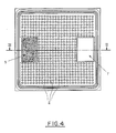
- the silicon contacts were opened into the oxide in the emitter regions, thus creating single cells forming emitter regions 2.
- the silicon is also caused to emerge on the base region surrounding the cells or emitter regions 2, so that an oxide annulus remains around each cell 2. This is obtained by masking with resist said oxide annulus in order that it is preserved and insulates the base-emitter junction on its surface.
- the oxide area 4 reserved for the emitter bond pad is also masked, in order that it remains insulated from the underlying N+ doped region.
- the area 5 for the base bond pad is on the contrary uncovered to have the successive contact with the base metallization.
- the base region 1 can have a depth of 10 ⁇ , whereas the emitter cells 2 have a diameter of 80 ⁇ and a depth of 5 ⁇ , said values being purely indicative.
- the metallization of the transistor is realized as two vertically offset metal layers, with the interposition between the metals of an insulating layer of polyimide.
- a suitable metal for metallization is an aluminium-silicon alloy which can be applied, for example, by means of sputtering.
- the first layer of metallization is thus applied onto a structure such as that shown in figure 1 and successively, by means of photolythographic removal, the metal of this layer, indicated with the number 6 in figure 3, is left on the base bond pad area 5 and on the emitter cells 2, being on the contrary removed from the emitter bond pad area 7.
- polyimide is an ideal dielectric, as it allows the employment of usual techniques and apparatuses, of relatively low cost and high efficiency.
- polyimide can be applied by means of a spin coating process, that is to say using the same method with which photoresists are usually deposited. This allows a surface topography to be obtained, which is as far as possible planar, before the deposition of the second metal layer.
- the layer of polyimide indicated with 8 in figure 3 is then treated by means of a photolythographic process to remove the imide from the base and emitter bond pad areas, indicated respectively with 5 and 7, and from the emitter cells 2.
- the polyimide layer 8 thus remains above the first metal layer, in the base region disposed around the emitter cells 2 and having a mesh configuration.
- a second layer of metallization indicated with 9 is applied, also preferably by means of sputtering, onto the first metal layer 6 and the polyimide layer 8, where this remains.
- the second metal layer 9 therefore serves to connect the emitter regions 2 with the emitter bond pad areas 7, as well as to form a thicker metal layer on the base bond pad area 5.
- base bond pad area 5 and the emitter bond pad area 7 must be ohmically insulated, so that the second metal layer 9 will be removed by means of a photolythographic tecnique along a strip all around the base bond pad area 5.
- the metal used for the second metallization can be a different metal from that used for the first metallization, or else the same metal as that used for the first, in particular silicon-aluminium alloy.
- the cell or emitter 2 can have a diameter of 30 ⁇ on an emitter doped region having a diameter of 80 ⁇ .
- the oxide ring 3 around the emitter shows typically an internal diameter of 30 ⁇ and an external diameter of 130 ⁇ , with a superposition of the first metal layer 6 on the oxide of about 20 ⁇ in a radial direction.
- the first metallization can have a thickness of around 3 ⁇ and the second metallization can have a thickness of 6 ⁇ , while the interposed polyimide layer can have a thickness of from about 3 to 3,6 ⁇ .
- the process by which the silicon/metal contacts are obtained in the process according to the invention is of fundamental importance for the efficiency of the device. As there are two distinct layers of metallization for base and emitter, the respective contacts must be formed in two separate moments. It must be noted that in order to obtain contacts with low resistivity it is necessary that the surface of the silicon should not have been damaged and that it be free from deposits and native oxide.
- the first metallization layer covers, along with the base areas around the cells 2, also the open contacts within the cells themselves. This enables the silicon to be physically sealed and protected from contaminations and damage during the successive phases of formation of the emitter contact. In fact, according to the invention, the contacts are opened in a single phase both for the base and for the emitter. This sequence allows optimization of the metal/silicon contact resistence within the emitter cell and furthermore the surface offered for deposition of the second metallization layer is much flatter. In this way an eventual thinning of the metal in correspondence with the edges of the emitter cell is avoided.
- the thermal treatment after patterning of the first metal layer performs both the base and the emitter ohmic contact between silicon and metal.
- the emitter electric contact is then realized in the form of a metal/metal contact.
- a transistor obtained in the above described manner shows notable characteristics from the point of view of robustness and switching speed.
- the matrix cell configuration which allows optimal balancing of the structure, eliminates the presence of focusing points of the emitter current and of consequent failures due to Is/b (direct secund breakdown) or Es/b (inverse secund breakdown).
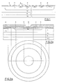
- FIG 4 a wafer is illustrated with the matrix configuration of emitter cells.
- the base bond pad 5 and the emitter bond pad 7 are also clearly seen.
- the electric measurements of dynamic type show that the cellular structure according to the present invention is by far more rapid, for example than a hollow emitter structure, reaching fall speeds in the order of several tens of nanoseconds.
- the storage also shows itself to be more rapid than in a hollow emitter device in the same conditions.
- the multicellular structure produced according to the invention has optimum behaviour also in RBSOA, being capable of switching 7 amgingre beyond the breakdown voltage with open base, both in voltage and current extraction.
- the object of the invention has been attained of producing a semiconductor device manufactured with low-cost techniques, also having a performance comparable to that of conventional semiconductor devices manufactured according to more sophisticated techniques.
Landscapes
- Bipolar Transistors (AREA)
- Thyristors (AREA)
Applications Claiming Priority (2)
| Application Number | Priority Date | Filing Date | Title |
|---|---|---|---|
| IT8806611A IT1234517B (it) | 1988-05-05 | 1988-05-05 | Dispositivo a semiconduttore bipolare di potenza e procedimento per la sua fabbricazione |
| IT661188 | 1988-05-05 |
Publications (3)
| Publication Number | Publication Date |
|---|---|
| EP0341221A2 true EP0341221A2 (de) | 1989-11-08 |
| EP0341221A3 EP0341221A3 (en) | 1990-08-22 |
| EP0341221B1 EP0341221B1 (de) | 1994-08-03 |
Family
ID=11121393
Family Applications (1)
| Application Number | Title | Priority Date | Filing Date |
|---|---|---|---|
| EP89830186A Expired - Lifetime EP0341221B1 (de) | 1988-05-05 | 1989-05-03 | Bipolarer Leistungshalbleiteranordnung und Verfahren zur ihrer Herstellung |
Country Status (5)
| Country | Link |
|---|---|
| US (1) | US5032887A (de) |
| EP (1) | EP0341221B1 (de) |
| JP (1) | JPH0216740A (de) |
| DE (1) | DE68917197T2 (de) |
| IT (1) | IT1234517B (de) |
Cited By (3)
| Publication number | Priority date | Publication date | Assignee | Title |
|---|---|---|---|---|
| EP0666600A3 (de) * | 1994-02-02 | 1996-04-10 | Rohm Co Ltd | Leistungs-Bipolartransistor. |
| EP0557705A3 (en) * | 1992-02-24 | 1997-07-09 | Motorola Semiconducteurs | Fabrication of lateral bipolar transistor |
| WO2005015641A1 (en) * | 2003-08-02 | 2005-02-17 | Zetex Plc | Biopolar transistor with a low saturation voltage |
Families Citing this family (6)
| Publication number | Priority date | Publication date | Assignee | Title |
|---|---|---|---|---|
| JPH0490514A (ja) * | 1990-08-02 | 1992-03-24 | Semiconductor Energy Lab Co Ltd | 半導体装置 |
| SE516226C2 (sv) * | 1995-04-10 | 2001-12-03 | Forskarpatent I Linkoeping Ab | Bipolära transistorer med extra bas-kollektor- och bas- emitterstrukturer |
| US7598521B2 (en) * | 2004-03-29 | 2009-10-06 | Sanyo Electric Co., Ltd. | Semiconductor device in which the emitter resistance is reduced |
| US9331186B2 (en) | 2009-12-21 | 2016-05-03 | Nxp B.V. | Semiconductor device with multilayer contact and method of manufacturing the same |
| JP7514389B2 (ja) * | 2020-09-03 | 2024-07-10 | ヒタチ・エナジー・リミテッド | パワー半導体デバイス |
| US20230223393A1 (en) * | 2022-01-13 | 2023-07-13 | Texas Instruments Incorporated | Semiconductor devices with high current capability for electrostatic discharge or surge protection |
Family Cites Families (15)
| Publication number | Priority date | Publication date | Assignee | Title |
|---|---|---|---|---|
| US3381183A (en) * | 1965-06-21 | 1968-04-30 | Rca Corp | High power multi-emitter transistor |
| US4008484A (en) * | 1968-04-04 | 1977-02-15 | Fujitsu Ltd. | Semiconductor device having multilayered electrode structure |
| US3843425A (en) * | 1971-04-05 | 1974-10-22 | Rca Corp | Overlay transistor employing highly conductive semiconductor grid and method for making |
| US4291319A (en) * | 1976-05-19 | 1981-09-22 | National Semiconductor Corporation | Open base bipolar transistor protective device |
| JPS5397379A (en) * | 1977-02-07 | 1978-08-25 | Fujitsu Ltd | Transistor |
| US4581626A (en) * | 1977-10-25 | 1986-04-08 | General Electric Company | Thyristor cathode and transistor emitter structures with insulator islands |
| US4417265A (en) * | 1981-03-26 | 1983-11-22 | National Semiconductor Corporation | Lateral PNP power transistor |
| JPS57160160A (en) * | 1981-03-27 | 1982-10-02 | Nippon Denso Co Ltd | Semiconductor device |
| JPS5943830B2 (ja) * | 1981-10-23 | 1984-10-24 | 株式会社東芝 | 圧接型半導体装置 |
| FR2545654B1 (fr) * | 1983-05-03 | 1985-09-13 | Fairchild Camera Instr Co | Composant semi-conducteur de puissance, et procede pour la fabrication |
| JPS601846A (ja) * | 1983-06-18 | 1985-01-08 | Toshiba Corp | 多層配線構造の半導体装置とその製造方法 |
| JPS60132366A (ja) * | 1983-12-21 | 1985-07-15 | Toshiba Corp | 半導体装置 |
| DE3573357D1 (en) * | 1984-12-27 | 1989-11-02 | Siemens Ag | Semiconductor power switch |
| US4656496A (en) * | 1985-02-04 | 1987-04-07 | National Semiconductor Corporation | Power transistor emitter ballasting |
| JPS6236305U (de) * | 1985-08-20 | 1987-03-04 |
-
1988
- 1988-05-05 IT IT8806611A patent/IT1234517B/it active
-
1989
- 1989-04-28 US US07/344,568 patent/US5032887A/en not_active Expired - Lifetime
- 1989-05-03 DE DE68917197T patent/DE68917197T2/de not_active Expired - Fee Related
- 1989-05-03 JP JP1113519A patent/JPH0216740A/ja active Pending
- 1989-05-03 EP EP89830186A patent/EP0341221B1/de not_active Expired - Lifetime
Cited By (6)
| Publication number | Priority date | Publication date | Assignee | Title |
|---|---|---|---|---|
| EP0557705A3 (en) * | 1992-02-24 | 1997-07-09 | Motorola Semiconducteurs | Fabrication of lateral bipolar transistor |
| EP0666600A3 (de) * | 1994-02-02 | 1996-04-10 | Rohm Co Ltd | Leistungs-Bipolartransistor. |
| US5637910A (en) * | 1994-02-02 | 1997-06-10 | Rohm Co., Ltd. | Multi-emitter or a multi-base transistor |
| WO2005015641A1 (en) * | 2003-08-02 | 2005-02-17 | Zetex Plc | Biopolar transistor with a low saturation voltage |
| US7923751B2 (en) | 2003-08-02 | 2011-04-12 | Zetex Plc | Bipolar transistor with a low saturation voltage |
| KR101045335B1 (ko) * | 2003-08-02 | 2011-06-30 | 지텍스 피엘씨 | 낮은 포화 전압을 갖는 쌍극성 트랜지스터 |
Also Published As
| Publication number | Publication date |
|---|---|
| IT8806611A0 (it) | 1988-05-05 |
| US5032887A (en) | 1991-07-16 |
| DE68917197T2 (de) | 1995-03-16 |
| DE68917197D1 (de) | 1994-09-08 |
| EP0341221A3 (en) | 1990-08-22 |
| JPH0216740A (ja) | 1990-01-19 |
| EP0341221B1 (de) | 1994-08-03 |
| IT1234517B (it) | 1992-05-19 |
Similar Documents
| Publication | Publication Date | Title |
|---|---|---|
| US4975782A (en) | Field effect controlled, bipolar power semiconductor component with silicide layer | |
| US5789311A (en) | Manufacturing method of SiC Schottky diode | |
| US4155155A (en) | Method of manufacturing power semiconductors with pressed contacts | |
| EP0341221B1 (de) | Bipolarer Leistungshalbleiteranordnung und Verfahren zur ihrer Herstellung | |
| KR920003467B1 (ko) | 트리밍소자와 그 전기단락방법 | |
| JPS6358376B2 (de) | ||
| US3210620A (en) | Semiconductor device providing diode functions | |
| US3280386A (en) | Semiconductor a.c. switch device | |
| EP0247660B1 (de) | Halbleiteranordnung mit einem Bipolartransistor und Feldeffekttransistoren | |
| JPH067592B2 (ja) | ゲ−トタ−ンオフサイリスタ | |
| KR930001460A (ko) | 반도체 집적회로장치 및 그 제조방법 | |
| JPH07273309A (ja) | 電力半導体素子 | |
| US3252063A (en) | Planar power transistor having all contacts on the same side thereof | |
| JPS6156628B2 (de) | ||
| SE509780C2 (sv) | Bipolär effekttransistor och framställningsförfarande | |
| GB1415810A (en) | Switching networks and switches for use therein | |
| JP2622521B2 (ja) | ゲート遮断サイリスタ及びその製造方法 | |
| CA1205577A (en) | Semiconductor device | |
| US6858887B1 (en) | BJT device configuration and fabrication method with reduced emitter width | |
| US3736478A (en) | Radio frequency transistor employing high and low-conductivity base grids | |
| US3713008A (en) | Semiconductor devices having at least four regions of alternately different conductance type | |
| US4058887A (en) | Method for forming a transistor comprising layers of silicon dioxide and silicon nitride | |
| JP2974583B2 (ja) | 半導体装置およびその製造方法 | |
| EP0420164B1 (de) | Verfahren zur Herstellung einer Halbleiteranordnung mit mehrschichtiger Elektrodenstruktur | |
| US3979767A (en) | Multilayer P-N junction semiconductor switching device having a low resistance path across said P-N junction |
Legal Events
| Date | Code | Title | Description |
|---|---|---|---|
| PUAI | Public reference made under article 153(3) epc to a published international application that has entered the european phase |
Free format text: ORIGINAL CODE: 0009012 |
|
| AK | Designated contracting states |
Kind code of ref document: A2 Designated state(s): DE FR GB NL |
|
| PUAL | Search report despatched |
Free format text: ORIGINAL CODE: 0009013 |
|
| RHK1 | Main classification (correction) |
Ipc: H01L 29/08 |
|
| AK | Designated contracting states |
Kind code of ref document: A3 Designated state(s): DE FR GB NL |
|
| 17P | Request for examination filed |
Effective date: 19901128 |
|
| 17Q | First examination report despatched |
Effective date: 19930705 |
|
| GRAA | (expected) grant |
Free format text: ORIGINAL CODE: 0009210 |
|
| AK | Designated contracting states |
Kind code of ref document: B1 Designated state(s): DE FR GB NL |
|
| PG25 | Lapsed in a contracting state [announced via postgrant information from national office to epo] |
Ref country code: NL Effective date: 19940803 |
|
| REF | Corresponds to: |
Ref document number: 68917197 Country of ref document: DE Date of ref document: 19940908 |
|
| ET | Fr: translation filed | ||
| NLV1 | Nl: lapsed or annulled due to failure to fulfill the requirements of art. 29p and 29m of the patents act | ||
| PLBE | No opposition filed within time limit |
Free format text: ORIGINAL CODE: 0009261 |
|
| STAA | Information on the status of an ep patent application or granted ep patent |
Free format text: STATUS: NO OPPOSITION FILED WITHIN TIME LIMIT |
|
| 26N | No opposition filed | ||
| REG | Reference to a national code |
Ref country code: FR Ref legal event code: D6 |
|
| REG | Reference to a national code |
Ref country code: GB Ref legal event code: IF02 |
|
| PGFP | Annual fee paid to national office [announced via postgrant information from national office to epo] |
Ref country code: GB Payment date: 20020501 Year of fee payment: 14 |
|
| PGFP | Annual fee paid to national office [announced via postgrant information from national office to epo] |
Ref country code: FR Payment date: 20020508 Year of fee payment: 14 Ref country code: DE Payment date: 20020508 Year of fee payment: 14 |
|
| PG25 | Lapsed in a contracting state [announced via postgrant information from national office to epo] |
Ref country code: GB Free format text: LAPSE BECAUSE OF NON-PAYMENT OF DUE FEES Effective date: 20030503 |
|
| PG25 | Lapsed in a contracting state [announced via postgrant information from national office to epo] |
Ref country code: DE Free format text: LAPSE BECAUSE OF NON-PAYMENT OF DUE FEES Effective date: 20031202 |
|
| GBPC | Gb: european patent ceased through non-payment of renewal fee |
Effective date: 20030503 |
|
| PG25 | Lapsed in a contracting state [announced via postgrant information from national office to epo] |
Ref country code: FR Free format text: LAPSE BECAUSE OF NON-PAYMENT OF DUE FEES Effective date: 20040130 |
|
| REG | Reference to a national code |
Ref country code: FR Ref legal event code: ST |