EP0341097B1 - Rekursiver Addierer zur Berechnung der Summe zweier Operanden - Google Patents
Rekursiver Addierer zur Berechnung der Summe zweier Operanden Download PDFInfo
- Publication number
- EP0341097B1 EP0341097B1 EP89400604A EP89400604A EP0341097B1 EP 0341097 B1 EP0341097 B1 EP 0341097B1 EP 89400604 A EP89400604 A EP 89400604A EP 89400604 A EP89400604 A EP 89400604A EP 0341097 B1 EP0341097 B1 EP 0341097B1
- Authority
- EP
- European Patent Office
- Prior art keywords
- adder
- carry
- output
- bit
- propagation
- Prior art date
- Legal status (The legal status is an assumption and is not a legal conclusion. Google has not performed a legal analysis and makes no representation as to the accuracy of the status listed.)
- Expired - Lifetime
Links
Images


Classifications
-
- G—PHYSICS
- G06—COMPUTING OR CALCULATING; COUNTING
- G06F—ELECTRIC DIGITAL DATA PROCESSING
- G06F7/00—Methods or arrangements for processing data by operating upon the order or content of the data handled
- G06F7/38—Methods or arrangements for performing computations using exclusively denominational number representation, e.g. using binary, ternary, decimal representation
- G06F7/48—Methods or arrangements for performing computations using exclusively denominational number representation, e.g. using binary, ternary, decimal representation using non-contact-making devices, e.g. tube, solid state device; using unspecified devices
- G06F7/50—Adding; Subtracting
- G06F7/505—Adding; Subtracting in bit-parallel fashion, i.e. having a different digit-handling circuit for each denomination
- G06F7/506—Adding; Subtracting in bit-parallel fashion, i.e. having a different digit-handling circuit for each denomination with simultaneous carry generation for, or propagation over, two or more stages
- G06F7/508—Adding; Subtracting in bit-parallel fashion, i.e. having a different digit-handling circuit for each denomination with simultaneous carry generation for, or propagation over, two or more stages using carry look-ahead circuits
Definitions
- the present invention relates to a recursive type adder for calculating the sum of two operands.
- This invention applies to the calculation of the sum of two numbers of binary data using adders constituted in the form of integrated circuits, in particular for information processing systems in which these adders constitute one of the fundamental processing operators. of the signal.
- the invention falls into the category of parallel-parallel type adders. They make it possible to add two operands A and B respectively made up of binary data a1, a2, ..., a n and b1, b2, ..., b n . The result is provided in parallel binary form.
- a parallel-parallel adder is constituted by a complex association of series of elementary adders connected together.
- Each elementary adder receives two bits to be added which belong to each of the operands or to intermediate results carried out by other elementary adders of the complex circuit.
- Each adder provides on an output the binary result of an addition but can also provide, on two other outputs, two so-called propagation and generation bits, respectively.
- a k and b k respectively denote the input bits of rank k, to be added.
- the generation function G k of an adder AD k corresponds to an output bit of this adder, equal to 1, each time a carry-over appears during the addition.
- the propagation function P k corresponds to an output bit of this adder, equal to 1, when a carry from an adder of the previous rank (k-1), must be propagated to the adder of the next rank (k + 1).
- S k P k ⁇ r k-1
- r1IN the incoming carry applied to the first adder in the series
- rKOUT the outgoing carry applied by the last adder in the series.
- parallel adders can be of two types: adders of the "iterative" type and those of the "recursive" type. In these two types of adders, the propagation of the carry is the essential problem.
- an adder for n bits is constructed, by adding an elementary cell (full adder or full adder), to an adder already comprising n-1 elementary cells connected in series.
- This structure translates the recurrence relation of the addition.
- the classic example of such a type of adder is the Manchester type carrier with Manchester carry chain.
- n-bit adder In a recursive type adder, an n-bit adder is subdivided into two n / 2-bit adders.
- the propagation time of the carry is theoretically Log (n) T, if T designates the propagation time for an elementary cell.
- This recursive structure is essentially used in adders using tree structures which allow the necessary information to be distributed to the different cells in an optimized time.
- This type of adder is often referred to as a carry look ahead adder.
- iterative type adders require less silicon for their manufacture, but they are slower than recursive type adders which consume a lot of silicon.
- One of these known compromise solutions is an optimized carry select adder.
- This solution consists in cutting the addition into several slices. For each of these tranches, we make assumptions, as indicated above, on the withholding entering each tranche.
- the incoming carry in each slice is determined step by step using a series of cells which perform the logical operation g.r + p; in this relation, g is a bit which indicates whether or not there is generation of carry, r designates a carry bit, and p is a bit which indicates whether or not there is propagation of the carry.
- This type of adder can be qualified as a g.r + p type adder.
- the adder whose incoming carry is equal to zero has the outgoing carry generated by the slice, which is designated by G t .
- the adder whose inbound holdback is equal to 1 has its own calculated holdback for outbound holdback.
- the calculations are carried out in parallel in the different slices and the optimization of an adder of this type relates to the number of bits that each slice must calculate to make all the propagation paths critical, in a structure of adders in a tree, of predetermined hierarchical level. Definitions concerning critical paths, tree structures and hierarchical levels are given in the aforementioned reviews.
- the number of elementary addition cells can be gradually increased in each new slice, so that the calculation time required for a slice is equal to that of the previous slice, increased by the time selection method. In this case, an optimized carry-over selection adder is obtained.
- This adder has a drawback compared to the previous one: to make all the critical paths, both for the sum to be calculated and for the carry, it is necessary, going from low weights to high weights of bits to be added, to increase the size slices (that is to say the number of elementary adders in series in each slice), then decrease this size from the middle of the adder.
- the reduction in the size of the tranches is indeed essential in order to avoid that the deduction is obtained too quickly compared to the sum S.
- the size of the slices increases in linear progression.
- the sum selection time varies on the assumption of a selection time equal to a propagation time through a Full-Adder.
- n n + 1 / 2 bits in a time nT
- n2 / 2 bits are calculated in nT
- n bits are calculated in ⁇ 2 nT (T denoting the time required to calculate the addition of two data bits).
- the size of the slices increases in linear progression for the first half of the bits to be added and then decreases in the same way.
- n bits in a time 2 ⁇ nt .
- Optimized solutions such as the carry jump adder or the carry selection adder, are an interesting compromise but are not entirely satisfactory: they do not allow, while retaining an occupied surface close to that of a carry jump adder, achieve the speed performance of a carry selection adder.
- the object of the invention is to remedy these drawbacks and in particular to produce an adder occupying a surface close to that of a carry-jump adder, while exhibiting a performance in speed close to that of a carry-through adder .
- the adder of the invention presents, as will be seen in detail below, a new structure called recursive, which makes it possible to obtain a particularly high speed / surface merit factor.
- AD adder NH K with recursive structure represented schematically in FIG. 1 presents a level NH of recursion and an order K.
- the NH level (NH being an integer) is in fact the number of recursions that it is necessary to perform to construct an adder having a structure of NH level, from a structure of level NH-1, and so continued up to level 1.
- Such adders have a tree structure, the different branches of which comprise series of complete adders.
- AD adder NH K represented in this figure makes it possible to calculate the sum of two operands A and B formed respectively of binary data a1, a2, a i , a n and b1, b2, b i , b n (with 1 ⁇ i ⁇ n) having different weights .
- These two operands can themselves consist of a first and a second operand AL and BL formed respectively of binary data a! i and b i of least significant and a third and fourth operand AN and BH formed respectively by the binary data a i and b i of most significant.
- AD adder NH K recursively includes a first adder of order K-1 and of NH level, built itself recursively.
- This first adder has inputs which receive the first and second least significant operands AL and BL respectively.
- a first output of this first adder provides the operand SL resulting from the summation of the operands AL and BL received as input.
- a second output from this first adder provides an outgoing carry COUT bit, resulting from the summing performed.
- AD adder NH K also has a second adder of order K-1 and of level NH-1 constructed also recursively.
- This second adder has inputs which respectively receive the third and fourth operands AH and BH constituted by the most significant data.
- An input CIN of this adder, called "incoming hold" is connected to the second output of the first adder to receive the outgoing carry COUT bit from this first adder.
- This second adder also comprises a first output which provides an operand SH for summing the third and fourth operands AH and BH of the most significant data received as input.
- a second output of this second adder provides a bit P of propagation of the carry while a third output provides a bit G of generation of the carry resulting from the summation.
- the adder AD NH K includes a SE restraint selector.
- This carry selector has three inputs 1, 2, 3 which are respectively connected to the second output of the first adder and at the second and third outputs of the second adder to receive the bits COUT, P and G respectively.
- This carry selector provides on an output, a global output carry bit of the adder AD NH K considered.
- Figure 2 shows schematically and in more detail the second adder of order K-1 and of level NH-1 of figure 1. This figure makes it possible to better understand the recursion of the structure of the adder of figure 1.
- the second adder which is shown in Figure 2 is itself built recursively and has a third adder noted of order K-2 and level NH-2.
- This third adder has inputs which respectively receive operands AHL and BHL respectively constituted by least significant data contained in the third and fourth operands AH and BH.
- An incoming CIN input from this third adder and which is also the CIN input from the second adder described above, is connected to the second output of the first adder to receive the outgoing carry COUT bit from this first adder.
- the third adder comprises first, second and third outputs which respectively provide an SHL operand for summing the AHL and BHL operands received as input, a bit G1 for outgoing carry generation and a bit P1 for outgoing carry propagation of the summation carried out by this third adder .
- the second adder also includes a first SES intermediate hold selector which has three inputs. These three inputs are respectively connected to the second output of the first adder and at the second and third outputs of the third adder to receive the bits COUT, G1 and P1 respectively.
- This first intermediate retention SES selector provides, on an output, a C1OUT bit for outgoing retention for the summation performed by the third adder.
- the + sign designates an "INCLUSIVE OR" and the sign ".” a logical "AND”.
- the second adder has a fourth adder of order K-2 and level NH-2, a second intermediate selector SEC and an output logic "AND" gate.
- the fourth adder has inputs receiving respectively operands AHH and BHH respectively constituted by most significant data of the third and fourth operands AH and BH described above.
- a C2IN input from the fourth adder is connected to the output of the first intermediate SES selector to receive the carry bit outgoing C1OUT provided by this first intermediate selector.
- the fourth adder also includes first, second and third outputs which respectively provide an operand SHH for summing the input operands AHH and BHH, a bit G2 for carry generation and a bit P2 for carry propagation for the summation carried out by this fourth adder.
- the second intermediate selector SEC provides a carry bit G, which is the outgoing carry bit of the second adder
- the second SEC selector has three inputs which are respectively connected to the second generation output of the third adder at the second generation output of the fourth adder and at the third propagation output of the fourth adder, to receive the bits G1, G2 and P2 respectively.
- This second intermediate selector SEC provides on a hold generation output, which is also the second output of the second adder the carry generation bit G.
- FIG. 3 shows schematically the ADP adder 1 K of order K and level 1.
- This adder is obtained recursively from the adder of order K-1 and level NH-1. It allows adding two by two of the bits of a data slice ai, a i + 1 , ..., a i + j ... a i + K , and b i , b i + 1 , ... b i + j , ... b i + k , of a data slice of the two operands A and B (i being between 1 and n).
- This adder comprises at least K elementary addition cells, of the "full adders" type. These cells are represented in FA i , FA i + 1 , ...
- the cell FA i has two inputs for receiving the bits a i and b j respectively .
- the bits a j and b j are also applied to two inputs of the cell FA i + j
- the bits a K and b K are applied to two inputs of the cell FA i + K.
- Each elementary addition cell also has an incoming carry input for receiving an outgoing carry bit supplied by a first carry out output from a previous addition cell, from the succession of cells.
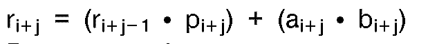
- the complete cell or adder FA i + j has an input E i + j which receives an incoming carry bit r i + j-1 coming from a first output of the adder FA i + j-1 previous (not shown in the figure).
- an input E i + 2 of the adder FA i + 2 receives an outgoing carry bit r i + 1 from a first output of the previous adder FA i + 1 .
- Each elementary cell such as FA i + j also has first and second outputs which respectively provide a local summation bit s i + j and a local propagation bit P i + j .
- the ADP adder 1 K shown in the figure also includes a logic assembly CP for calculating the propagation of the carry for this adder.
- This set includes inputs which are respectively connected to the second and third outputs of the elementary cells FA i , FA i + 1 , ... FA i + j , ... FA i + K.
- This set therefore receives the local summation bits s i , s i + 1 , ... s i + j , ... s i + K , and the local propagation bits p i , p i + 1 , ... p i + K , ... p i + K.
- P i K of propagation of the carry, for this ADP adder 1 K .
- the propagation calculation set CP includes logic gates of the "AND" type denoted ET i + 1 , ET i + 2 , ... AND i + K in the figure. Each of these doors has two entrances.
- the two inputs of the first AND gate i + 1 are respectively connected to the propagation outputs pi and p i + 1 of the first pair of cells FA i , FA i + 1 .
- the AND gate i + 2 has two inputs which are respectively connected to the third propagation output p i + 2 of the cell FA i + 2 and to the output of the preceding AND gate i + 1 .
- the AND gate i + K has two inputs which are respectively connected to the third propagation output of the cell FA i + K and to the output of the preceding AND gate i + K-1 .
- P i + j P i + d-1 .p i + j .
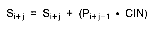
- the ADP adder 1 K also includes a logical set CS of summation calculation, which provides, on outputs, operands S i , S i + 1 , ..., S i + j , ..., S i + K for summing the binary data received on the first inputs of the adder.
- This set includes inputs which are respectively connected to the second outputs s i , s i + 1 , ..., s i + j , ..., s i + K of the elementary cells FA i , FA i + 1 , .. ., FA i + j , ..., FA i + K.
- This summation calculation set CS also includes an incoming retention CIN entry.
- the summation calculation set CS provides on its outputs, the summing operands of the data (a i , b i ), (a i + 1 , b i + 1 ), ... (a i + K , b i + K ) received as input.
- the summation calculation set CS comprises logic gates M i , M i + 1 , ..., M i + j , ..., M i + K of AND type with two inputs and logic gates OR i , OR i + 1 , ..., OR i + j , ..., OR i + K of type "OR EXCLUSIVE" with two inputs.
- each OR gate i + j are respectively connected to the output of the corresponding gate M i + j as well as to the second output S i + j of the corresponding elementary cell.
- the OR gate i + 1 is connected to the output of the gate M i + 1 and at the output s i + 1 of the elementary cell FA i + 1 .
- S i + 2 s i + 2 ⁇ (P i + 1 .CIN)
- ADP adders 1 K which process slices of data bits from i to i + K (or i belongs to ⁇ 1, 2, .., n ⁇ )
- the number i depends on the position of the adder ADP 1 K in the tree which constitutes the adder AD NH K .
- ADP adders 1 K have at least k elementary addition cells.
- FIG. 4 schematically represents the adder AD 1 K of order K and level 1.
- This adder taking into account the recursive structure described above, is in fact constituted by an adder ADP 1 K of order K and level 1, whose incoming carry input CIN receives a bit of value 0.
- One of the outputs of this adder provides the generation bit G, while its carry propagation output P does not is not connected.
- AD adder 1 K starting point may or may not have a non-zero CIN input depending on whether one wishes to make a global adder with zero or non-zero incoming carry.
Landscapes
- Physics & Mathematics (AREA)
- General Physics & Mathematics (AREA)
- Engineering & Computer Science (AREA)
- Computational Mathematics (AREA)
- Mathematical Analysis (AREA)
- Pure & Applied Mathematics (AREA)
- Theoretical Computer Science (AREA)
- Computing Systems (AREA)
- Mathematical Optimization (AREA)
- General Engineering & Computer Science (AREA)
- Complex Calculations (AREA)
Claims (4)
- Rekursiver Addierer zum Berechnen der Summe zweier Operanden A und B, die jeweils aus Binärdaten a₁ , a₂ ..., an und b₁, b₂ ..., bn verschiedenen Gewichts gebildet sind, wobei die Operanden A und B einen ersten und einen zweiten Operanden AL und BL umfassen, jeweils gebildet aus Daten schwachen Gewichts, sowie einen dritten und einen vierten Operanden AH und BH, jeweils gebildet aus Daten starken Gewichts, dadurch gekennzeichnet, daß für ein Rekursivniveau NH des Addierers und eine Ordnung K dieses Addierers dieser Addierer als ADK NH bezeichnet wird, wobei NH eine ganze Zahl größer oder gleich 1 ist und die Anzahl der Niveaurekursivitäten angibt, die ausgeführt werden müssen, um eine Struktur von Niveau NH aus einer Struktur von NH-1, usw. bis zum Niveau 1, zu bilden, K eine ganze Zahl ist, welche die Anzahl von Additions-Elementarzellen in einem Addierer von Niveau 1 angibt, und K>2 ist, wobei der Addierer ADK NH umfaßt:- einen ersten Addierer ADK NH der Ordnung K-1 und von Niveau NH, umfassend Eingänge, die den ersten bzw. zweiten Operanden AL bzw. BL schwachen Gewichts erhalten, einen ersten Ausgang, welchen einen Summationsoperanden des ersten und zweiten Operanden AL und BL niedrigen Gewichts liefert, und einen zweiten Ausgang, der ein Ausgangsübertragsbit COUT für die ausgerührte Summe liefert;- einen zweiten Addierer ADPK-1 NH-1 der Ordnung K-1 und von Niveau NH-1, umfassend Eingänge, die einen dritten bzw. vierten Operanden AH bzw. BH starken Gewichts erhalten, einen Eingang (CIN), der mit dem zweiten Ausgang (COUT) des ersten Addierers verbunden ist, und einen ersten, einen zweiten und einen dritten Ausgang, die einen Summationsoperanden SH des dritten und vierten Operanden AH und BH starken Gewichts, ein Übertrags-Propagationsbit P, das dieser Summe entspricht, bzw. ein Bit G liefern, das die Generation des Übertrags darstellt;- einen globalen Übertragswähler (SE), umfassend drei Eingänge (1, 2, 3), verbunden mit dem zweiten Ausgang (COUT) des ersten Addierers und dem zweiten bzw. dritten Ausgang (G, P) des zweiten Addierers, und einen Ausgang, der ein globales Übertragsbit COUT NH aus der logischen Summe liefert:

- Addierer nach Anspruch 1, dadurch gekennzeichnet, daß der zweite Addierer ADPK-1 NH-1 umfaßt:- einen dritten Addierer ADPK-2 NH-1 der Ordnung K-2 und von Niveau NH-2, umfassend Eingänge, die Operanden AHL bzw. BHL erhalten, die gebildet sind aus Daten schwachen Gewichts des dritten bzw. des vierten Operanden AH bzw. BH, und einen Eingang (CIN) zur Übertragseingabe, verbunden mit dem zweiten Ausgang des ersten Addierers, um das vom ersten Addierer ausgegebenen Übertragsbit (COUT) zu empfangen, und einen ersten, zweiten und dritten Ausgang, um einen Summationsoperanden (SHL) der eingegebenen Operanden AHL und BHL, ein Bit (G1), das die Übertragsgeneration darstellt, bzw. ein Übertragspropagationsbit (P1) der ausgeführten Summe zu liefern;- einen ersten Übertrags-Zwischenwähler (SES), umfassend drei Eingänge, die mit dem zweiten Ausgang (COUT) des ersten Addierers, dem zweiten Ausgang (G1) des dritten Addierers, bzw. des dritten Ausgangs (P1) des dritten Addierers verbunden sind, wobei der erste Übertragswähler an seinem Ausgang ein Ausgangsübertragsbit C₁OUT liefert, das der logischen Summe folgt:

- einen vierten Addierer ADPK-2 NH-2 der Ordnung K-2 und von Niveau NH-2, umfassend Eingänge, die Operanden AHH bzw. BHH erhalten, die gebildet sind aus Daten starken Gewichts des dritten bzw. vierten Operanden, einen Eingang (C2IN) für den Eingangsübertrag, verbunden mit dem Ausgang des ersten Wählers (SES), um ein Ausgangsübertragsbit (C1OUT) dieses Wählers zu erhalten, und einen ersten, zweiten und dritten Ausgang, die einen Summationsoperanden (SHH) der im Eingang empfangenen Operanden (AHH und BHH), ein Bit (G2), das die Übertragsgeneration darstellt, und einen Übertrags-Propagationsoperanden (P2) der ausgeführten Summe liefern;- einen zweiten Zwischenwähler (SEC) für die Übertragsgeneration, umfassend drei Eingänge, die verbunden sind mit dem zweiten Ausgang (G1) für die Übertragsgeneration des dritten Addierers, dem zweiten Ausgang (G2) für die Übertragsgeneration des vierten Addierers, bzw. den dritten Ausgang (P2) für die Übertragspropagation des vierten Addierers, wobei der zweite Wähler an einem Ausgang, der dem dritten Ausgang des zweiten Addierers entspricht, daß Übertragsgenerationsbit (G) des zweiten Addierers liefert, welches aus der logischen Summe entsteht:

- ein logisches "UND"-Gatter mit zwei Eingängen, die mit dem dritten Propagationsausgang (P2) des vierten Addierers, bzw. dem dritten Propagationsausgang (P1) des dritten Addierers verbunden sind, wobei dieses logische Gatter über einen dem zweiten Ausgang des zweiten Addierers entsprechenden Ausgang das Ausgangs-Propagationsbit P des zweiten Addierers liefert, welches aus der logischen Multiplikation

- Addierer nach Anspruch 2, dadurch gekennzeichnet, daß der Addierer ADPK¹ der Ordnung K und von Niveau 1, rekursiv vom Addierer ADPK-1 NH-1 der Ordnung K-1 und von Niveau NH-1 ausgehend erhalten und geeignet zum paarweisen Addieren von bits aus Datenabschnitten ai, ai+1, ..., ai+j, ai+K, und bi, bi+1, ..., bi+j, bi+K der beiden Operanden A und B (wobei i zwischen 1 und n), umfaßt:- eine Folge von mindestens K Additions-Elementarzellen vom Typ "Vollständige Addierer", wobei jede Zelle (FAi+j) vom Rang i-j zwei Eingänge umfaßt, um ein Bitpaar wie (ai+j, bi+j ) zu erhalten, einen Eingangsübertragseingang, um ein Ausgangsübertragsbit (ri+j-1) zu erhalten, welches von einem ersten Übertragsausgang einer vorgeschalteten Zellelementarzelle FAi+j-i der entsprechenden Folge erhalten wird, wobei der Eingangsübertrags-Eingang der ersten Elementarzellen der betreffenden Folge ein Bit vom Wert 0 erhält und der Ausgangsübertrags-Ausgang der letzten Elementarzelle der betreffenden Folge ein Übertragsgenerationsbit (G) für die betreffende Folge liefert, wobei jede Elementarzelle (FAi+j) außerdem einen zweiten und einen dritten Ausgang umfaßt, die ein lokales Summationsbit Si+j bzw. ein Propagationsbit pi+j liefern, wobei sich die Bits ri+j, Si+j und Pi+j aus den logischen Operationen ergeben:


wobei · der "UND"-Operator ist, + der Operator "INKLUSIVES ODER" ist und ⊕ der Operator "EXCLUSIVES ODER" ist;- eine logische Baugruppe (CP) zum Berechnen der Übertragspropagation P des Addierers, umfassend Eingange, die jeweils mit dem dritten Propagationsausgängen (pi+j) der Elementarzellen verbunden sind, um über einen Ausgang ein Propagationsbit pi+K für den Addierer ADPK¹ zu liefern, das sich aus der logischen Operation ergibt:

oder

- eine logische Baugruppe (CS) zur Summationsberechnung, umfassend Eingänge, die mit zweiten Summationsausgängen der Elementarzellen bzw. Propagationsausgängen Pi+j der Propagationsbaugruppe (CP) verbunden sind, die bits
mit
Pi-1 = 1 - Addierer nach Anspruch 3, dadurch gekennzeichnet, daß der Addierer ADK¹ der Ordnung K und von Niveau 1 wie ein Addierer ADPK¹ der Ordnung K und von Niveau 1 aufgebaut ist, dessen Eingangsübertrags-Eingang (CIN) ein Bit (CIN) erhält, das gleich 0 ist.
Applications Claiming Priority (2)
| Application Number | Priority Date | Filing Date | Title |
|---|---|---|---|
| FR8802867A FR2628232B1 (fr) | 1988-03-07 | 1988-03-07 | Additionneur de type recursif pour calculer la somme de deux operandes |
| FR8802867 | 1988-03-07 |
Publications (2)
| Publication Number | Publication Date |
|---|---|
| EP0341097A1 EP0341097A1 (de) | 1989-11-08 |
| EP0341097B1 true EP0341097B1 (de) | 1993-11-03 |
Family
ID=9363972
Family Applications (1)
| Application Number | Title | Priority Date | Filing Date |
|---|---|---|---|
| EP89400604A Expired - Lifetime EP0341097B1 (de) | 1988-03-07 | 1989-03-03 | Rekursiver Addierer zur Berechnung der Summe zweier Operanden |
Country Status (5)
| Country | Link |
|---|---|
| US (1) | US4942549A (de) |
| EP (1) | EP0341097B1 (de) |
| JP (1) | JPH02153424A (de) |
| DE (1) | DE68910375T2 (de) |
| FR (1) | FR2628232B1 (de) |
Families Citing this family (6)
| Publication number | Priority date | Publication date | Assignee | Title |
|---|---|---|---|---|
| GB8904392D0 (en) * | 1989-02-27 | 1989-04-12 | Ibm | An arithmetic logic unit for a graphics processor |
| JPH0391832A (ja) * | 1989-09-05 | 1991-04-17 | Sony Corp | 加算回路 |
| KR100197354B1 (ko) * | 1995-06-28 | 1999-06-15 | 김영환 | 클럭 위상을 이용한 캐리증가 가산기 |
| JPH09231055A (ja) * | 1996-02-27 | 1997-09-05 | Denso Corp | 論理演算回路及びキャリールックアヘッド加算器 |
| DE10215784A1 (de) * | 2002-04-10 | 2003-10-30 | Infineon Technologies Ag | Rechenwerk und Verfahren zum Subtrahieren |
| DE10215785A1 (de) * | 2002-04-10 | 2003-10-30 | Infineon Technologies Ag | Rechenwerk und Verfahren zum Addieren |
Family Cites Families (3)
| Publication number | Priority date | Publication date | Assignee | Title |
|---|---|---|---|---|
| EP0164450B1 (de) * | 1983-12-27 | 1990-03-07 | Nec Corporation | Eine, für eine arithmetische Operation hoher Geschwindigkeit geeignete, Übertragsschaltung |
| JPS6149233A (ja) * | 1984-08-17 | 1986-03-11 | Nec Corp | 高速デジタル加減算回路 |
| US4623982A (en) * | 1985-06-10 | 1986-11-18 | Hewlett-Packard Company | Conditional carry techniques for digital processors |
-
1988
- 1988-03-07 FR FR8802867A patent/FR2628232B1/fr not_active Expired - Lifetime
-
1989
- 1989-03-03 EP EP89400604A patent/EP0341097B1/de not_active Expired - Lifetime
- 1989-03-03 DE DE89400604T patent/DE68910375T2/de not_active Expired - Fee Related
- 1989-03-07 US US07/320,319 patent/US4942549A/en not_active Expired - Fee Related
- 1989-03-07 JP JP1054828A patent/JPH02153424A/ja active Pending
Also Published As
| Publication number | Publication date |
|---|---|
| JPH02153424A (ja) | 1990-06-13 |
| DE68910375T2 (de) | 1994-05-11 |
| DE68910375D1 (de) | 1993-12-09 |
| US4942549A (en) | 1990-07-17 |
| EP0341097A1 (de) | 1989-11-08 |
| FR2628232B1 (fr) | 1994-04-08 |
| FR2628232A1 (fr) | 1989-09-08 |
Similar Documents
| Publication | Publication Date | Title |
|---|---|---|
| EP0692762B1 (de) | Logikschaltung zur parallelen Multiplikation | |
| EP0262032B1 (de) | Binärer Addierer mit festem Operand und paralleler/serieller Multiplikator mit solchen Addierern | |
| EP1190344B1 (de) | Multiplizierer für komplexe zahlen | |
| FR2662829A1 (fr) | Multiplicateur parallele utilisant un reseau de saut et un arbre de wallace modifie. | |
| EP0341097B1 (de) | Rekursiver Addierer zur Berechnung der Summe zweier Operanden | |
| EP0437876B1 (de) | Programmierbarer serieller Multiplikator | |
| EP0110767B1 (de) | Schneller binärer Multiplizierer | |
| BE898544R (fr) | Calculateur associatif permettant une multiplication rapide. | |
| EP0309348B1 (de) | Binäre Additions- und Multiplikationsvorrichtung | |
| EP0283393A1 (de) | Binäre Rechnungseinrichtung | |
| EP2013705B1 (de) | N-bit-addierer und dazugehöriges additionsverfahren | |
| EP0175623A1 (de) | Einrichtung zur Echtzeitdigitalsignalverarbeitung durch Faltung | |
| FR2599526A1 (fr) | Additionneur mos et multiplicateur binaire mos comprenant au moins un tel additionneur | |
| FR2563349A1 (fr) | Multiplieur matriciel systolique de traitement de donnees numeriques | |
| EP0128072B1 (de) | Binärer Multiplizierer mit Zeichenausbreitung für die Multiplikation von Zahlen mit oder ohne Zeichen | |
| EP0065460B1 (de) | Parallelzähler in integrierter MOS-Schaltung und seine Anwendung in einem Binäraddierer | |
| EP0205523B1 (de) | Einrichtung zur simultanen aktivierung von befehlsfolgen und ihre verwendung in speichern | |
| EP0655685B1 (de) | Einrichtung zum Berechnen von Paritätsbits in Verbindung mit einer Summe zweier Zahlen | |
| EP1335277B1 (de) | Effiziente sättigende Operation | |
| FR2516675A1 (fr) | Cellule d'addition binaire a trois entrees a propagation rapide de la retenue | |
| EP0718755A1 (de) | Elektronisches Bauelement, insbesondere fähig zum Ausführen einer Division zur Basis 4 von zwei Zahlen | |
| EP1439637A1 (de) | Anordung zur gemeinsamen Verarbeitung von Daten | |
| EP0332504B1 (de) | Verfahren zur Bestimmung der Struktur eines baumförmigen Zellenmultiplizierers, genannt in der p-ten Wurzel | |
| FR2734675A1 (fr) | Circuit logique combinatoire | |
| FR2545957A1 (en) | High-throughput binary multiplier |
Legal Events
| Date | Code | Title | Description |
|---|---|---|---|
| PUAI | Public reference made under article 153(3) epc to a published international application that has entered the european phase |
Free format text: ORIGINAL CODE: 0009012 |
|
| AK | Designated contracting states |
Kind code of ref document: A1 Designated state(s): DE GB IT NL SE |
|
| 17P | Request for examination filed |
Effective date: 19900414 |
|
| 17Q | First examination report despatched |
Effective date: 19920717 |
|
| RAP1 | Party data changed (applicant data changed or rights of an application transferred) |
Owner name: FRANCE TELECOM |
|
| GRAA | (expected) grant |
Free format text: ORIGINAL CODE: 0009210 |
|
| AK | Designated contracting states |
Kind code of ref document: B1 Designated state(s): DE GB IT NL SE |
|
| PG25 | Lapsed in a contracting state [announced via postgrant information from national office to epo] |
Ref country code: IT Free format text: LAPSE BECAUSE OF FAILURE TO SUBMIT A TRANSLATION OF THE DESCRIPTION OR TO PAY THE FEE WITHIN THE PRE;WARNING: LAPSES OF ITALIAN PATENTS WITH EFFECTIVE DATE BEFORE 2007 MAY HAVE OCCURRED AT ANY TIME BEFORE 2007. THE CORRECT EFFECTIVE DATE MAY BE DIFFERENT FROM THE ONE RECORDED.SCRIBED TIME-LIMIT Effective date: 19931103 Ref country code: NL Effective date: 19931103 Ref country code: SE Effective date: 19931103 |
|
| REF | Corresponds to: |
Ref document number: 68910375 Country of ref document: DE Date of ref document: 19931209 |
|
| GBT | Gb: translation of ep patent filed (gb section 77(6)(a)/1977) |
Effective date: 19931207 |
|
| NLV1 | Nl: lapsed or annulled due to failure to fulfill the requirements of art. 29p and 29m of the patents act | ||
| PLBE | No opposition filed within time limit |
Free format text: ORIGINAL CODE: 0009261 |
|
| STAA | Information on the status of an ep patent application or granted ep patent |
Free format text: STATUS: NO OPPOSITION FILED WITHIN TIME LIMIT |
|
| 26N | No opposition filed | ||
| PGFP | Annual fee paid to national office [announced via postgrant information from national office to epo] |
Ref country code: GB Payment date: 19970225 Year of fee payment: 9 |
|
| PGFP | Annual fee paid to national office [announced via postgrant information from national office to epo] |
Ref country code: DE Payment date: 19970310 Year of fee payment: 9 |
|
| PG25 | Lapsed in a contracting state [announced via postgrant information from national office to epo] |
Ref country code: GB Free format text: LAPSE BECAUSE OF NON-PAYMENT OF DUE FEES Effective date: 19980303 |
|
| GBPC | Gb: european patent ceased through non-payment of renewal fee |
Effective date: 19980303 |
|
| PG25 | Lapsed in a contracting state [announced via postgrant information from national office to epo] |
Ref country code: DE Free format text: LAPSE BECAUSE OF NON-PAYMENT OF DUE FEES Effective date: 19981201 |