EP2013705B1 - N-bit-addierer und dazugehöriges additionsverfahren - Google Patents
N-bit-addierer und dazugehöriges additionsverfahren Download PDFInfo
- Publication number
- EP2013705B1 EP2013705B1 EP07731319.5A EP07731319A EP2013705B1 EP 2013705 B1 EP2013705 B1 EP 2013705B1 EP 07731319 A EP07731319 A EP 07731319A EP 2013705 B1 EP2013705 B1 EP 2013705B1
- Authority
- EP
- European Patent Office
- Prior art keywords
- rank
- bit
- sum
- estimated
- input
- Prior art date
- Legal status (The legal status is an assumption and is not a legal conclusion. Google has not performed a legal analysis and makes no representation as to the accuracy of the status listed.)
- Ceased
Links
Images


Classifications
-
- G—PHYSICS
- G06—COMPUTING OR CALCULATING; COUNTING
- G06F—ELECTRIC DIGITAL DATA PROCESSING
- G06F7/00—Methods or arrangements for processing data by operating upon the order or content of the data handled
- G06F7/38—Methods or arrangements for performing computations using exclusively denominational number representation, e.g. using binary, ternary, decimal representation
- G06F7/48—Methods or arrangements for performing computations using exclusively denominational number representation, e.g. using binary, ternary, decimal representation using non-contact-making devices, e.g. tube, solid state device; using unspecified devices
- G06F7/50—Adding; Subtracting
- G06F7/505—Adding; Subtracting in bit-parallel fashion, i.e. having a different digit-handling circuit for each denomination
- G06F7/506—Adding; Subtracting in bit-parallel fashion, i.e. having a different digit-handling circuit for each denomination with simultaneous carry generation for, or propagation over, two or more stages
-
- G—PHYSICS
- G06—COMPUTING OR CALCULATING; COUNTING
- G06F—ELECTRIC DIGITAL DATA PROCESSING
- G06F2207/00—Indexing scheme relating to methods or arrangements for processing data by operating upon the order or content of the data handled
- G06F2207/506—Indexing scheme relating to groups G06F7/506 - G06F7/508
- G06F2207/5063—2-input gates, i.e. only using 2-input logical gates, e.g. binary carry look-ahead, e.g. Kogge-Stone or Ladner-Fischer adder
-
- G—PHYSICS
- G06—COMPUTING OR CALCULATING; COUNTING
- G06F—ELECTRIC DIGITAL DATA PROCESSING
- G06F7/00—Methods or arrangements for processing data by operating upon the order or content of the data handled
- G06F7/38—Methods or arrangements for performing computations using exclusively denominational number representation, e.g. using binary, ternary, decimal representation
- G06F7/48—Methods or arrangements for performing computations using exclusively denominational number representation, e.g. using binary, ternary, decimal representation using non-contact-making devices, e.g. tube, solid state device; using unspecified devices
- G06F7/50—Adding; Subtracting
- G06F7/505—Adding; Subtracting in bit-parallel fashion, i.e. having a different digit-handling circuit for each denomination
- G06F7/506—Adding; Subtracting in bit-parallel fashion, i.e. having a different digit-handling circuit for each denomination with simultaneous carry generation for, or propagation over, two or more stages
- G06F7/508—Adding; Subtracting in bit-parallel fashion, i.e. having a different digit-handling circuit for each denomination with simultaneous carry generation for, or propagation over, two or more stages using carry look-ahead circuits
Definitions
- the invention relates to digital adders, in particular adders formed from cascaded half-adders.
- two half-adders are used cascaded.
- the first adder performs the sum of the two bits and outputs the result of the sum and a first intermediate hold.
- the second half-adder receives as input the incoming carry and the result of the sum obtained previously and delivers, on the one hand, the sum of the incoming retainer and the two input bits, and on the other hand, the final hold. .
- each bit of rank n of the sum of the two input numbers is estimated and corrected n times by the successive deductions generated at each half-adders stage.
- this type of standard adder requires propagating each retaining generated at each processing stage, which may be unnecessary for some applications, for example in the case of the use of half-adders to perform divisions.
- the document US 3,566,098 relates to a conventional binary number adder circuit.
- the bits of the sum of input signals are estimated and corrected after each estimation by the successive detentions generated at each stage of the circuit.
- the invention aims to provide a solution to these problems.
- said estimates ( U j ) are corrected using a correction signal ( R j ) after each estimation, each rank correction bit (n) R not j , being developed using the latest estimate of the rank bit not - 1 ⁇ U not - 1 j - 1 , the last bit of rank correction not - 1 ⁇ R not - 1 j - 1 , and the last estimate of the rank bit (n-2) ( U not - 2 j - 1 ) .
- This method has the advantage of being able to make corrections either negative or positive at each estimate of the bits of the sum. Processes using iterative additions / subtractions are improved.
- the input signals may further include an input retainer.
- the method further comprises an initialization step where the value of the estimated bits of said sum and the value of the correction signals are initialized, and j successive processing steps, j being an integer less than or equal to N, or during the k th stage, k varying from 1 to j, the bits of the sum whose rank n is between k and N are estimated, and for each bit of rank n, the n th correction signal is calculated, each estimated bit of the sum of rank n, being estimated from the estimated bit of the sum of rank n and the n th correction signal respectively estimated and elaborated during the preceding step, the n th correction signal, being developed from the estimated bits of the sum of rank n-1 and rank n-2, and the (n-1) th of the correction signal, respectively estimated and developed in the previous step.
- an output restraint can be developed from all N th correction signals.
- the initialization of each estimated bit of said sum is a function of the bits of the same rank of the first and second input numbers, and the initialization of the value of the correction signal of each estimated bit is function of the previous rank bits of the first and second input numbers.
- the initialization of each estimated bit of said sum is a function of the complement of the bit of the same rank of the first input number
- the initialization of the value of the correction signals of each estimated bit is a function of the previous rank bit of the first input number, and the bit of the same rank of the second input number.
- the initialization of the signals according to this embodiment has the advantage of being compatible with the reversibility logic.
- j is equal to N, and the bit of rank n of said sum, corresponds to the estimated bit of rank n of the sum, estimated during the n th processing step.
- the method further comprises, at the end of the processing steps, a step of generating N-1 propagation signals, the qth propagation signal being a function of the estimated bit of said sum. of rank q, its correction signal, and the estimated bit of rank q-1 of said sum, and wherein each bit of said sum is calculated from the qth propagation signals, such that q is less than the rank of bit considered.
- an adder for adding input signals according to claim 11.
- the input signals may further include an input retainer.
- each estimation block of a bit of the sum of rank n comprises a logic gate of the "EXCLUSIVE OR" adapted to receive as input the estimated bit of the sum of rank n and the n th correction signal respectively estimated and elaborated by the (k-1) th processing means, and in which the means for correcting an estimated bit of the sum of rank n + 1 comprise another gate “EXCLUSIVE OR” logic, able to receive as input the estimated and corrected bit of the sum of rank n-1, and the bit of rank (n-2) of the sum estimated and elaborated by the (k-1) the second processing means, and an "AND” type logic gate coupled to the output of the other "EXCLUSIVE OR” type logic gate, and adapted to receive as input the output signal of said other logic gate and the (n -1) th estimated correction signal and produced by the (k-1) th processing means.
- the processing means may furthermore comprise processing means capable of producing an output restraint from all the N th correction signals.
- the initialization means are able to initialize the value of each bit to estimate of said sum as a function of the bits of the same rank of the first and second input numbers, and able to initialize the value of the correction signal of each bit to be estimated based on the previous rank bits of the first and second input numbers.
- the initialization means comprise N elementary initialization means, each being associated with a given rank, comprising an "EXCLUSIVE OR" type logic gate, able to receive the bits of the rank considered of the first and second input numbers, and able to deliver for the rank in question, the initial value of the bit to be estimated of the sum, and a logical gate of the "AND" type, able to receive the bits of the rank considered, of the first and second numbers of input, and able to output the initial value of the correction signal of the estimated bit of the sum, the rank following the row considered.
- N elementary initialization means each being associated with a given rank, comprising an "EXCLUSIVE OR" type logic gate, able to receive the bits of the rank considered of the first and second input numbers, and able to deliver for the rank in question, the initial value of the bit to be estimated of the sum, and a logical gate of the "AND” type, able to receive the bits of the rank considered, of the first and second numbers of input, and able to output the initial value of the correction
- the initialization means comprise N elementary initialization means, each associated with a given rank, comprising an inverting logic gate, able to receive the bits of the rank considered of the first input number, and capable of delivering, for the rank in question, the initial value of the bit to be estimated from the sum, and an EXCLUSIVE logic gate with an inverting output, able to receive the bit of the rank considered of the first input number and the bit of the rank following the rank considered of the second entry number, and able to deliver the initial value of the correction signal of the estimated bit of the sum, of the rank according to the rank considered.
- j is equal to N, and the bit of the sum of rank n, corresponds to bit of the sum of rank n estimated by the nth processing means.
- the adder further comprises generating means coupled to the j th processing means, adapted to generate N-1 spread signals, the q th propagation signal being a function of the estimated bit of said sum of rank q, of its correction signal, and the estimated bit of rank q-1 of said sum, and calculation means able to calculate each bit of said sum from the q th propagation signals, such that q is less than the rank of the bit considered.
- the generation means can generate an N th propagation signal as a function of the estimated bit of rank N, its correction signal and the estimated bit of rank N-1.
- the calculation means may furthermore comprise a calculation block that can calculate a group generation term from the set of generated propagation signals and the set of correction signals, and a group propagation term from of all the propagation signals.
- a system comprising an adder network according to the first aspect of the invention.
- the system may comprise an adder network incorporating adders according to the first or second variant.
- the system may comprise an adder network incorporating N / 4 adders according to the third variant and the various embodiments thereof, (and such that the input signals comprise a restraint input), coupled in parallel, each adder being able to add N / 4 successive bits of the first and second input binary number.
- Said system may furthermore comprise at least one group propagation module (MPGi) able to receive the group generation term and the group propagation term of each adder, and able to elaborate from the group generation term and the group propagation term of a given adder, a carry for the adder adding the next N / 4 bits.
- MPGi group propagation module
- a simple and iterative calculation structure can also be obtained by integrating into the system a second bit level adder network in which the correction signal is cascaded from the rank module (n) to the rank module (n + 1). ) on the model known as "Ripple-Carry-Adder" in the Anglo-Saxon language known to those skilled in the art.
- FIG. 1 represents a flowchart with the different steps of an embodiment of a method according to the invention.
- step 1 different signals R n-1 0 , U n-1 0 are initialized, implemented to produce the sum of two binary numbers, 2 respectively A (a 0 , .. ., a n-1 ) and B (b 0 , ... b n-1 ) and a possible retention Z in .
- A a 0 , .. ., a n-1
- B b 0 , ... b n-1
- step 2 the previously calculated signals R and U are corrected and then a new estimate is made (step 2, correction and new estimation of R n + 1 j , U n + 1 j ).
- step 2 the bit of the sum of the input signals (A, B, Z in ) of rank n, Sn is generated.
- step 3 the value of i is incremented by one unit (step 3, i i + 1), then steps 2 and 3 are reiterated so as to generate all the bits of the sum S .
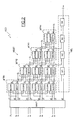
- the reference ADD designates an adder according to one embodiment of the invention. It comprises MDET determination means adapted to receive an input hold Z in at the input and two binary input numbers A and B each having in this example four bits, respectively at 0 , ... a 3 and b 0. , ... b 3 .
- the set of bits as well as the input hold Z in are delivered to MINIT initialization means.
- the MINIT initialization means initialize the signals R and U according to an algorithm described in more detail below.
- the initialisation means MINIT deliver at the output respectively the signals U 0 0, ..., U 3 0 0 and R 0, ..., R 3 0.
- the initialization means further MINIT deliver the signals U 0 -1 which initialization will be detailed in greater detail hereinafter and R 4 0 which corresponds to a first estimation of the output value of the adder ADD.
- the initialisation means MINIT are connected to a first stage of treatment MTR1 adapted to output a first bit of the estimation of the sum S, which correspond to the signals U 0 1, ..., U 3 1 and the correction signal these estimated bits of the sum, which are respectively the signals R 1 1 , ..., R 3 1 .
- the estimated bits of the sum U 0 1 , ..., U 3 1 are respectively estimated from estimation blocks BEST1, ... BEST4.
- the first stage treatment also outputs a correction signal R 4 1 of the carry output R 4 0.
- the correction signals R 1 1 ,..., R 4 1 are respectively produced using correction means, respectively MCOR1,... MCOR4.
- the first processing stage MTR1 delivers the first bit S0 of the sum S, which corresponds to the first estimate of this bit, that is to say U 0 1 .
- the MDET determination means comprise a second MTR2 processing stage. It incorporates the correction means MCOR5, MCOR6 and MCOR7 and estimation blocks BEST5, BEST6 and BEST7.
- the latter respectively deliver the correction signals R 2 2 ,..., R 4 2 and the estimated bits of the sum U 1 2 , ..., U 3 2 .
- the estimated bit U 1 2 corresponds to the second bit of the sum S1.
- Third MTR3 processing means are connected to the output of MTR2 means. These means MTR3 comprise correction blocks MCOR8 and MCOR9 and estimation means BEST8 and BEST9.
- the latter deliver the correction signals R 3 3 and R 4 3 and the estimated bits U 2 3 , which corresponds to the third bit of the sum S 2, and U 3 3 .
- the processing means are connected to the output of MTR3 processing means and comprises the correction means and the MCOR10 BEST10 estimation block, respectively delivering the correction signal R 4 4 and the estimated bit U 3 4, the latter corresponding at the last bit of the sum S3.
- Each of the correction means MCOR 1, i ranging from 1 to 10, delivering a correction signal R n j receives as input the signals U n-1 j-1 , U n-2 j-1 and the correction signal R n- 1 j-1 , n and j varying in this example from 0 to 3.
- the signal U -1 0 (defined below) is input, so as to develop the correction signal R 1 1 .
- the determination means also comprise MEL production means, comprising four means M1, M2, M3 and M4 connected in series.
- the means Mi i varying in this case from 1 to 4, receive as input the output signal of the means Mi-1 and the correction signal R 4 i .
- M1 means receive as input the first estimate of the carry output, that is to say R 4 0 issued by the initialization means MINIT.
- the means M4 output the final value of the output hold Z out .
- each estimation block BESTi incorporated in a stage of rank n, n varying from 0 to 3, and i varying from 1 to 10, comprises an "EXCLUSIVE OR" type logic gate.
- the correction means MCORi of a stage of rank n comprise a logic gate of the "EXCLUSIVE OR" type, referenced XORi, able to receive the estimated bit of the sum U n-1 j-1 and the estimated bit of the sum U n-2 j-1 .
- the MOCORi means comprise a logic gate of "ET" type, referenced ETi, and adapted to receive the output signal delivered by the logic gate XORi and the correction signal R n-1 j-1 .
- the means M1, M2, M3 M4 are each made from an "EXCLUSIVE OR" type logic gate.
- the figure 3 illustrates a first embodiment of the MINIT initialization means.
- the correction signal R 0 0 corresponds to the input hold Z in .
- variable U -1 0 is assigned here the value "0".
- the MINIT initialization means comprise four elementary initialization means ME1, ..., ME4.
- Each means MEi i varying here from 1 to 4, comprises an "EXCLUSIVE OR” type logic gate and an “AND” type logic gate respectively referenced XORii and ETii. Each of these gates respectively receives the bits of the input numbers a n-1 and b n-1 .
- Each logic gate ETii outputs the correction signal R n 0 .
- Each logic gate XORii outputs an initial value of the estimated bit U n-1 0 .
- This embodiment of the implementation of these new initialization means has the advantage of being compatible with the reversibility logic.
- the elementary initialization means MEi each comprise an inverting gate INViii, i varying from 1 to 4, capable of receiving the bit a n-1 and of delivering the initial value of the estimated bit of the sum U n. -1 0 .
- the MEi means further comprises a logic gate of the "EXCLUSIVE OR" at inverting output, referenced XORiii and receiving as input the bit a n-1 and the bit b n.
- Each logic gate XORiii outputs the correction signal R n 0 .
- the logic gate XOR444 receives in input instead of the bit of the second input number B, the binary value "0".
- the XOR444 cell is connected to the MEL generating means via another inverting gate INV5.
- the correction signal R 0 0 is delivered by a logic gate of the "EXCLUSIVE OR" type with an inverting output, referenced XOR000, receiving as input the retaining Z in and the input bit b 0 .
- the initialization variable U -1 0 is delivered by an inverting gate INV000 receiving as input the hold Z in .
- the determination means MDET comprising the initialization means represented on the FIG. figure 4 .
- the initialization values U n 0 and R n 0 are calculated according to the expressions defined above. Then a first estimate of the sum S is made by calculating the bits U n 1 . Then, the correction signals R n 1 are determined . These steps are successively repeated for the other bits of the sum S. Finally, the sum S is equal to 1000. We then find our in the case of a standard carry propagation.
- the system in question may comprise a first adder and a second adder.
- the first adder receives as input the first and second binary numbers A and B, respectively, and outputs a sum A + B.
- the second adder receives as input the intermediate sum A + B and the third binary number C and generates a sum S corresponding to the sum of the three input binary numbers A, B and C.
- the system For each additional bit number to be added, the system includes an additional adder.
- the embodiment of the MDET determination means represented on the figure 5 comprises generating means adapted to receive the signals U -1 j , U 0 j , R 0 j , ..., U 3 j , R 3 j .
- This embodiment of the MDET means is particularly suitable in the context of using an adder to perform a division.
- the generation means MGEN comprise a logic gate of "EXCLUSIVE OR" type, referenced XORiiii able to receive as input the signal U n j and the signal U n-1 j .
- the XORiiiii logic gate is connected to an "EXCLUSIVE" type logic gate with an inverting output, referenced NXORi.
- the logic gate NXORi receives as input the output signal delivered by the logic gate XORiiii and the signal R n j .
- the gate NXORi outputs the propagation signal t n j .
- the generation means MGEN are coupled to the output means for computing, so as to calculate the bits of the sum S, that is, S0, ..., S3.
- the S0 bit is then produced using an "EXCLUSIVE OR" type logic gate referenced XORS0. This receives as input the signal R 0 j and the estimated bit of the sum U 0 j .
- the S1 bit of the sum S is delivered by a logic gate of "EXCLUSIVE OR" type referenced XORS1. This receives as input the estimated bit of the sum U 1 j and the output signal of another logic gate of the type "EXCLUSIVE OR” referenced XORS12.
- the XORS12 gate receives as input the correction signal R 1 j and the output signal of a logic gate of "ET" type referenced ETS1. The latter receives as input the propagation signal t 0 j and the correction signal R 0 j .
- the S2 bit of the sum S is delivered by an XORS2 type "EXCLUSIVE OR” logic gate, which receives the estimated bit U 2 j as input and the output signal of another referenced "EXCLUSIVE OR” type logic gate.
- XORS22 The S2 bit of the sum S is delivered by an XORS2 type "EXCLUSIVE OR" logic gate, which receives the estimated bit U 2 j as input and the output signal of another referenced "EXCLUSIVE OR” type logic gate.
- the logic gate XORS22 receives as input the output signal of a logic gate of "EXCLUSIVE OR” type referenced XORS23 and the output signal of a logic gate of "ET” type referenced ETS21. The latter receives as input the propagation signal t 1 j and the correction signal R 1 j .
- the logic gate XORS23 receives as input the correction signal R 2 j and the output signal of another ETS22 type "ET" logic gate which receives as input propagation signals t 1 j and t 0 i and the signal correction number R 0 j .
- the S3 bit of the sum S is delivered by an XORS3 logic gate of the "EXCLUSIVE OR" type.
- This receives as input the estimated bit U 3 j and the output signal of another logic gate of the type "EXCLUSIVE OR" referenced XORS32.
- the logic gate XORS34 receives as input the correction signal R 3 j and the output signal of a logic gate of "ET" type referenced ETS33 which receives as input the propagation signals t 0 j , t 1 j and t 2 j and the correction signal R 0 j .
- the logic gate XORS33 referenced as input the output signals of two other doors of type "ET" respectively ETS31 and ETS32.
- the gate ETS31 receives as input the propagation signal t 2 j and the correction signal R 2 j .
- the logic gate ETS32 receives as input the propagation signals t 1 j and t 2 j and the correction signal R 1 j .
- the propagation signals produced by this type of determination means can be used within CLA type adders ("Carry-Look-Ahead" in English), to add 2n bits.
- CLA type adders Carry-Look-Ahead
- several means MDET are generated in parallel, able to generate propagation signals, in this case called group propagation signals, as well as group generation signals in the case of an addition of 2n bits as described hereinabove. after.
- the set of MDET means are combined with a so-called group propagation module well known to those skilled in the art (see for example the reference book “Advanced Computer Arithmetic Design” MJ Flynn, SF Oberman, 2001, Editions John Wiley and sons, ISBN 0-471-41209-0 pages 4 and 5).
- the group propagation module generates from the group generation signals and the group propagation signals generated by the means MDET which add the bits n, n + 1, n + 2 and n + 3 (for example), a retaining (or incoming generation term) for the MDET means that add the bits n + 4, n + 5, n + 6 and n + 7.
- the figure 6 represents means MDET used in the context of a coupling with other means MDET so as to form a type adder CLA able to add 2n bits.
- MDET means of the figure 6 are used to elaborate the terms Sn, ..., Sn + 3 of the sum S, and the so-called group generation and group propagation signals, respectively Z n + 3_i and t n + 3_i , for the module developing the term of incoming generation of the following MDET means, as explained below.
- the MGEN means of figure 6 furthermore, in comparison with the means represented on the figure 5 , a gate XORZn receiving as input the hold (incoming generation term) Zn generated by the MDET means connected upstream and the signal R j n .
- the output of the XORZn gate is connected to the gate input XORSn, ETSn + 1, ETSn + 1.2, ETSn + 3.3.
- the MGEN means comprise two logic gates XORn +3.333 and NXORn + 3, respectively of the "EXCLUSIVE OR” and "EXCLUSIVE OR” type with an inverting output.
- the gate XORn + 3,333 receives as input the signal U j n + 3 and U j n + 2 . Its output is connected to the input of the NXORn + 3 gate.
- the gate NXORn + 3 also receives the signal R j n + 3 as input and delivers another propagation signal t j n + 3 as output.
- bit Z n + 3_i is delivered by an XORZ3 logic gate of "EXCLUSIVE OR" type.
- the logic gate XORZ1 receives as input the output signals of two logic gates of type "AND" respectively referenced ETZ1 and ETZ2.
- the logic gate XORZ2 receives as input the output signals of two logic gates of type "AND" respectively referenced ETZ3 and ETZ4.
- the logic gate ETZ1 receives as input the propagation signal t n + 3 j and the correction signal R n + 3 j .
- the logic gate ETZ2 receives as input the propagation signals t n + 3 j and t n + 2 j and the correction signal R n + 2 j .
- the logic gate ETZ3 receives as input the propagation signals t n + 3 j and t n + 2 j , t n + 1 j and the correction signal R n + 1 j .
- the logic gate ETZ4 receives, as input, the propagation signals t n + 3 j t n + 2 j , t n + 1 j , t n j and the correction signal R n j .
- the MCAL means also comprise another logic gate of "ET" type, referenced ETt receiving as input the propagation signals t n + 3 j and t n + 2 j , t n + 1 j , t n j and delivering in output the signal t n + 3_i .
- figure 7 represents a multi-level adder and more precisely a 16-bit adder with group carry propagation.
- the 16-bit adder SYS comprises four blocks A 1 , A 2 , A 3 and A 4 corresponding to the means MDET as described in FIG. figure 6 .
- the first block A 1 receives as input the signals U j -1 , U j 0 , ..., U j 3 , R j 0 , ..., R j 3 and the input hold Z n (0 in this case), and outputs the first four bits of the resultant sum S 0 , .... S 3 , the generation signal per group Z 3_0 as defined in FIG. figure 6 , as well as the propagation signal by group T 3_0 (the signals U j -1 , U j 0 ,..., U j 3 , R j 0 ,..., R j 3 have been developed by means of initialization as described above, not shown here for simplification purposes).
- These signals are delivered to a group propagation module referenced MPG, which receives as input the resulting carry Z 3_0 of the first block A 1 , the group propagation signal t 3_0 and the input hold Z in .
- the MPG group propagation module elaborates the incoming generation term Z 4 of block A2.
- the blocks A 2, A 3 and A 4 respectively receive the input signals U j 4, ..., U j 7, R 4 j, ..., R j and U j 7 8 .. ., U j 11, R 8 j, ..., R j and U j 11 12, ..., U j 15, R 12 j, ..., R j 15 and the generation of terms incoming Z 4 , Z 8 and Z 12 produced by the MPG propagation module.
- the block A 2 outputs the bits S 4 , ... S 7 of the sum S
- the block A3 delivers the output bits S 8 , ..., S 11
- the block A 4 delivers the bits of the sum S 12 , ..., S 15 .
- the MPG module generates a resultant hold Z 16 , as well as a group propagation signal G 15_0 , and a group propagation signal T 15_0 .
- the signals G 15_0 and T 15_0 respectively correspond to the generation and group propagation signals of all the blocks A1,..., A4.
- the figure 8 also represents an adder with propagation of the retaining group receiving 64-bit input.
- This type of adder well known to those skilled in the art can be used with MDET means as described in the figure 5 as well as two levels of group propagation modules.
- the SYS system comprises a first level consisting of four MPG1, MPG2, MPG3 and MPG4 group propagation modules. Each group propagation module is connected to four sub-blocks, respectively A1, ..., A 4 and A 5 , ..., A 8 and A 9 , ... A 12 , and A 13 , ... , A 16 , corresponding to the MDET means represented on the figure 5 .
- the second level of group propagation module comprises an MPG5 module which receives as input the output signals delivered by each group propagation module of the first level.
- the adder as described above can be used in place of a conventional 64-bit adder, with group carry propagation in all configurations.
- the MDET means comprise MGEN generating means able to receive the signals U 1 j , U 0 j , R 0 j , ... , U 3 j , R 3 j .
- the MDET means further include MBIT means. These MBIT means perform the calculations at each bit and are attacked by the output signals of the generation means MGEN, the latter making it possible to accelerate the calculation of the output signals S0, S1, S2 and S3 and the outgoing carry-out Z out of said MBIT means.
- the signals Z 0 Z 1_0 Z and Z 2_0 3_0 are meanwhile holding signals which are transmitted between computing means MBIT.
- This simple and iterative embodiment of the MDET means is particularly compact and therefore suitable for use in an integrated circuit.
- each means MBIT of rank (n + 1) comprises a first logic gate “EXCLUSIVE OR” able to receive the retaining signal Z n-1_0 generated by the means MBIT of rank (n) and the correction signal R not j .
- the delivered signal attacks a logic AND logic gate which has for the second input the signal t not j from the MGEN means, the output of this gate "AND LOGIC" constituting the retaining signal Z n_0 propagated to the means MBIT of rank (n + 2).
- the MBIT means also comprises a second logic gate of "EXCLUSIVE OR” type receiving as a first input the signal generated by said first "EXCLUSIVE OR” gate and as a second input the signal U not j , and outputting the signal S n .
- a retaining signal Z out is generated by an "EXCLUSIVE" logic gate with an inverting output receiving as input the retaining signal Z 3_0 delivered by the means MBIT of rank 4 and the signal U 3 j .
Landscapes
- Engineering & Computer Science (AREA)
- Physics & Mathematics (AREA)
- General Physics & Mathematics (AREA)
- Theoretical Computer Science (AREA)
- Pure & Applied Mathematics (AREA)
- Mathematical Analysis (AREA)
- Computational Mathematics (AREA)
- Computing Systems (AREA)
- Mathematical Optimization (AREA)
- General Engineering & Computer Science (AREA)
- Error Detection And Correction (AREA)
- Compression, Expansion, Code Conversion, And Decoders (AREA)
- Complex Calculations (AREA)
Claims (28)
- Additionsverfahren für Eingangssignale durch einen digitalen Addierer, der Eingangssignale als eine erste und zweite Eingangsbinärzahl mit jeweils N Bits erfasst, bei denen der Addierer die Bits der Summe (Sn) der Eingangssignale (A, B) bestimmt, indem er j Schätzungen für jedes Bit der erwähnten Summe durchführt, wobei j eine Zahl unter oder gleich N darstellt, und die besagten Schätzungen (Uk) mithilfe eines Korrektursignals (Rk) nach jeder Schätzung konigiert, und zwar dahingehend, dass jedes Korrekturbit der Stufe


- Verfahren gemäß dem vorhergehenden Anspruch, in dem die Eingangssignale außerdem einen Eingangsübertrag (Zin) beinhalten.
- Verfahren gemäß einem der vorhergehenden Ansprüche, das außerdem eine Initialisierungsstufe (Stufe 1) umfasst, in der man den Wert der geschätzten Bits der erwähnten Summe und den Wert der Korrektursignale initialisiert.
- Verfahren gemäß einem der vorhergehenden Ansprüche, in dem man außerdem einen Ausgangsübertrag (Zout) auf der Grundlage der Nten Korrektursignale ermittelt.
- Verfahren gemäß einem der Ansprüche 3 bis 4, in dem die Initialisierung jedes geschätzten Bits der erwähnten Summe eine Funktion der Bits desselben Rangs der ersten und zweiten Eingangszahl (A, B) und die Initialisierung des Werts des Korrektursignals jedes geschätzten Bits eine Funktion der Bits der vorhergehenden Stufe der ersten und zweiten Eingangszahl darstellt.
- Verfahren gemäß dem vorhergehenden Anspruch, in dem:

wobei:
 an und bn Bits der Stufe n beziehungsweise die ersten und zweiten Eingangszahlen darstellen.
 - Verfahren gemäß einer der Ansprüche 3 bis 4, in dem die Initialisierung jedes geschätzten Bits der erwähnten Summe eine Funktion des Komplementärbits derselben Stufe der ersten Eingangszahl darstellt, und die Initialisierung des Werts der Korrektursignale jedes geschätzten Bits eine Funktion des Bits der vorhergehenden Stufe der ersten Eingangszahl und des Bits derselben Stufe der zweiten Eingangszahl darstellt.
- Verfahren gemäß dem vorhergehenden Anspruch, in dem:

wobei:
 an und bn Bits der Stufe n beziehungsweise der ersten und zweiten Eingangszahlen darstellen.
 - Verfahren gemäß einem der Ansprüche 3 bis 8, in dem j gleich N ist, und in dem das Bit der Stufe n der Summe (Sn) dem Bit der geschätzten Stufe der Summe entspricht, die bei dem (n+1)ten Bearbeitungsschritt

- Verfahren gemäß einem der Ansprüche 3 bis 8, das außerdem am Ende von j Bearbeitungsschritten einen Schritt der Erzeugung von N-1 Übertragungssignalen (tn, j) beinhaltet, wobei das qte Übertragungssignal eine Funktion des geschätzten Bits der erwähnten Summe der Stufe q, seines Korrektursignals und des geschätzten Bits der Stufe q-1 der erwähnten Summe darstellt, und in dem jedes Bit der erwähnten Summe aufgrund von qten Übertragungssignalen berechnet wird, so dass q unterhalb der Stufe des betroffenen Bits liegt.
- Ein Addierer, der ermöglicht, Eingangssignale einer ersten (A) und einer zweiten (B) Eingangs-Binärzahl mit jeweils N Bits zu addieren, und zwar dahingehend, dass der Addierer Bestimmungsmittel (MDET) enthält, die geeignet sind, die Bits der Summe der Eingangssignale zu bestimmen, die sich folgendermaßen zusammensetzen:- Schätzmittel, die seriell verschaltete Schätzblocks (BESTi) enthalten, bei denen jeder Schätzblock in der Lage ist, die Schätzung eines Bits der erwähnten Summe durchzuführen;- eine Schätzung der Stufe n

 - Korrekturmittel (MCORi), die imstande sind, ein Korrektursignal eines Bits der erwähnten Summe zu ermitteln;- ein Korrektursignal der Stufe n

- Addierer gemäß dem vorhergehenden Anspruch, bei dem die Eingangssignale außerdem einen Eingangsübertrag (Zin) beinhalten.
- Addierer gemäß einem der Ansprüche 11 bis 12, der außerdem vor den Bestimmungsmitteln eingeschaltete Initialisierungsmittel (MINIT) besitzt, die imstande sind, den Wert der geschätzten Bits der erwähnten Summe und den Wert der Korrektursignale zu initialisieren.
- Addierer gemäß dem vorhergehenden Anspruch, bei dem bzgl. der kten Bearbeitungsmittel jeder Schätzblock eines Bits der Summe der Stufe n ein XOR-Gatter enthält, das imstande ist, im Eingang ein geschätztes Bit der Summe der Stufe n und das nte Korrektursignal zu empfangen, die jeweils von den (k-1)ten Bearbeitungsmitteln geschätzt und ermittelt werden, und bei dem die Korrekturmittel eines geschätzten Bits der Summe der Stufe n+1 ein anderes XOR-Gatter enthält, das imstande ist, im Eingang das geschätzte und korrigierte Bit der Summe der Stufe n-1 und das mithilfe der (k-1)ten Bearbeitungsmittel geschätzte und ermittelte Bit der Stufe (n-2) zu empfangen; und ein anderes UND-Gatter, das mit dem Ausgang des anderen XOR-Gatters verschaltet und imstande ist, im Eingang das Ausgangssignal des erwähnten anderen logischen Gatters und das (n-1)te Korrektursignal zu empfangen, welches mithilfe der (k-1)ten Bearbeitungsmittel zu schätzen und zu ermitteln ist.
- Addierer gemäß einem der Ansprüche 12 bis 14, bei dem die Bearbeitungsmittel außerdem Ermittlungsmittel (MEL) enthalten, die imstande sind, einen Ausgangsübertrag (Zout) aufgrund aller Nten Korrektursignale zu ermitteln.
- Addierer gemäß einem der Ansprüche 13, 14, und 15, abhängig von 13, bei dem die Initialisierungsmittel (MINIT) imstande sind, den Wert jedes zu schätzenden Bits der erwähnten Summe in Einklang mit den Bits derselben Stufe der ersten und zweiten Eingangszahlen zu initialisieren, und imstande, den Wert des Korrektursignals jedes zu schätzenden Bits in Einklang mit den Bits der vorhergehenden Stufe der ersten und zweiten Eingangszahlen zu initialisieren.
- Addierer gemäß dem vorhergehenden Anspruch, bei dem die Initialisierungsmittel (MINIT) N elementare Initialisierungsmittel (MEi) enthalten, die jeweils mit einer gegeben Stufe verbunden sind, und der ein XOR-Gatter enthält, welches sowohl imstande ist, die Bits der betroffenen Stufe der ersten und zweiten Eingangszahlen zu empfangen, als auch für die betroffene Stufe den initialen Wert des zu schätzenden Bits der Summe zu liefern, und ein UND-Gatter, welches sowohl imstande ist, die Bits der betroffenen Stufe der ersten und zweiten Eingangszahlen zu empfangen, als auch den initialen Wert des Korrektursignals des geschätzten Bits der Summe der Stufe zu liefern, die auf die betroffene folgt.
- Addierer gemäß dem Anspruch 16, in dem die Initialisierungsmittel (MINIT) N elementare Initialisierungsmittel (MEi) beinhalten, wobei jedes mit einer gegebenen Stufe verknüpft ist, ein umkehrbares logisches Gatter enthält und imstande ist, die Bits der betroffenen Stufe der ersten Eingangszahl zu empfangen, sowie imstande, für die betroffene Stufe den initialen Wert des Bits der zu schätzenden Summe zu liefern, weiterhin ein XOR-Gatter am umkehrbaren Ausgang, das imstande ist, das Bit der betroffenen Stufe der ersten Eingangszahl und das Bit der Stufe zu empfangen, welches auf die betroffene Stufe der zweiten Eingangszahl folgt, sowie imstande, den initialen Wert des Korrektursignals des geschätzten Bits der Summe der Stufe, die auf die betroffene folgt.
- Addierer gemäß einem der Ansprüche 13 bis 18, in dem j gleich N ist und in dem das Bit der Summe der Stufe n dem Bit der Summe der Stufe n entspricht, das durch (n+1)te Bearbeitungsmittel geschätzt wird.
- Addierer gemäß einem der Ansprüche 13 bis 18, der außerdem mit den jten Bearbeitungsmitteln verschaltete Generierungsmittel (MGEN) enthält, die imstande sind, N-1 Übertragungssignale zu erzeugen, bei denen das qte Übertragungssignal eine Funktion des geschätzten Bits der erwähnten Summe der Stufe q, seines Korrektursignals und des geschätzten Bits der Stufe q-1 dieser Summe darstellt, sowie Berechnungsmittel (MCAL), die imstande sind, jedes Bit dieser Summe ausgehend von qten Übertragungssignalen zu berechnen, so dass q unterhalb der Stufe des betroffenen Bits liegt.
- Addierer gemäß dem Anspruch 20, in dem die Generierungsmittel (MGEN) imstande sind, ein ntes Übertragungssignal in Einklang mit dem geschätzten Bit der Stufe N, seinem Korrektursignal und dem geschätzten Bit der Stufe N-1 zu erzeugen, und in dem die Rechenmittel außerdem einen Rechenblock enthalten, der imstande ist, einen Gruppengenerierungsterm ausgehend von allen erzeugten Übertragungssignalen und allen Korrektursignalen, sowie einen Gruppenübertragungsterm ausgehend von allen Übertragungssignalen zu berechnen.
- Addierer gemäß dem vorhergehenden Anspruch, in dem N paarig ist und in dem der Rechenblock Folgendes enthält:- N logische UND-Gatter, worunter das qte Gatter, mit q variierend von 1 bis N, imstande ist, k Übertragungssignale, mit k variierend von 1 bis q,und das kte Korrektursignal zu empfangen;- ein Netz logischer XOR-Gatter, das imstande ist, alle von den Ausgängen der UND-Gatter gelieferten Terme zu addieren, um den erwähnten Generierungsgruppenterm zu ermitteln;- ein ergänzendes logisches UND-Gatter, das in der Lage ist, alle Übertragungssignale zu multiplizieren, um den erwähnten Übertragungsgruppenterm zu ermitteln.
- Addierer gemäß einem der Ansprüche 13 bis 18, der sich dadurch auszeichnet, dass die MDET-Mittel Generierungsmittel MGEN enthalten, die in der Lage sind, die Signale


- Addierer gemäß dem Anspruch 23, der sich dadurch auszeichnet, dass die Übertragungssignale


berechnet werden, mit n variierend von 1 bis 3 und j als eine beliebige ganze Zahl zwischen 0 und 3. - Addierer gemäß dem Anspruch 24, der sich dadurch auszeichnet, dass sich die Ausgangssignale S0, S1, S2, S3 durch die folgenden Relationen ergeben:

Mit:
- Addierer gemäß dem Anspruch 23, der sich dadurch auszeichnet, dass jedes Mittel MBIT der Stufe (n+1) ein erstes XOR-Gatter enthält, das imstande ist, den vom MBIT-Mittel der Stufe (n) generierten Signalübertrag Zn-1_0 und das Korrektursignal


- System, das sich aus einem Netz von Addierern gemäß einem der Ansprüche 11 bis 20 zusammensetzt.
- System gemäß dem Anspruch 27, in dem N ein Vielfaches von 4 ist und das Netz der Addierer gemäß der Kombination aus Anspruch 12 und einem der Ansprüche 21-22 N/4 Addierer (Ai) in Parallelschaltung verkörpert, wobei jeder Addierer imstande ist, N/4 aufeinanderfolgende Bits der ersten und zweiten Eingangsbinärzahlen zu addieren, und dieses System außerdem mindestens ein Übertragungsmodul pro Gruppe (MPGi) enthält, das imstande ist, den Gruppengenerierungsterm und den Gruppenübertragungsterm jedes Addierers zu empfangen, sowie imstande, ausgehend vom Gruppengenerierungsterm und Gruppenübertragungsterm eines gegebenen Addierers einen Übertrag für den Addierer zu ermitteln, der die folgenden N/4-Bits addiert.
Applications Claiming Priority (2)
| Application Number | Priority Date | Filing Date | Title |
|---|---|---|---|
| FR0603549A FR2900252B1 (fr) | 2006-04-21 | 2006-04-21 | Additionneur n bits et procede d'addition correspondant. |
| PCT/FR2007/000655 WO2007122319A1 (fr) | 2006-04-21 | 2007-04-19 | Additionneur n bits et procédé d'addition correspondant |
Publications (2)
| Publication Number | Publication Date |
|---|---|
| EP2013705A1 EP2013705A1 (de) | 2009-01-14 |
| EP2013705B1 true EP2013705B1 (de) | 2015-11-11 |
Family
ID=37680666
Family Applications (1)
| Application Number | Title | Priority Date | Filing Date |
|---|---|---|---|
| EP07731319.5A Ceased EP2013705B1 (de) | 2006-04-21 | 2007-04-19 | N-bit-addierer und dazugehöriges additionsverfahren |
Country Status (5)
| Country | Link |
|---|---|
| US (1) | US20090204659A1 (de) |
| EP (1) | EP2013705B1 (de) |
| JP (1) | JP2009534729A (de) |
| FR (1) | FR2900252B1 (de) |
| WO (1) | WO2007122319A1 (de) |
Families Citing this family (4)
| Publication number | Priority date | Publication date | Assignee | Title |
|---|---|---|---|---|
| FR2929726B1 (fr) * | 2008-04-02 | 2020-11-06 | S A R L Daniel Torno | Procede d'addition a operandes multiples, additionneur et produit programme d'ordinateur correspondants. |
| CN106528045B (zh) * | 2016-11-11 | 2018-12-04 | 重庆邮电大学 | 一种基于可逆逻辑门的4位可逆加/减法器 |
| TWI803126B (zh) * | 2021-12-30 | 2023-05-21 | 新唐科技股份有限公司 | 預看進位加法器、安全加法器以及執行預看進位加法的方法 |
| GB2634424A (en) * | 2022-05-11 | 2025-04-09 | Pablo Ramirez Juan | Simple and linear fast adder |
Family Cites Families (7)
| Publication number | Priority date | Publication date | Assignee | Title |
|---|---|---|---|---|
| GB1145676A (en) * | 1966-09-28 | 1969-03-19 | Nippon Electric Co | High speed adder circuit |
| GB8326690D0 (en) * | 1983-10-05 | 1983-11-09 | Secr Defence | Digital data processor |
| JPH09231055A (ja) * | 1996-02-27 | 1997-09-05 | Denso Corp | 論理演算回路及びキャリールックアヘッド加算器 |
| JP3322155B2 (ja) * | 1997-03-05 | 2002-09-09 | 日本電気株式会社 | データ再生装置 |
| US6298367B1 (en) * | 1998-04-06 | 2001-10-02 | Advanced Micro Devices, Inc. | Floating point addition pipeline including extreme value, comparison and accumulate functions |
| GB9817899D0 (en) * | 1998-08-17 | 1998-10-14 | Sgs Thomson Microelectronics | Designing addition circuits |
| WO2002008885A1 (en) * | 2000-07-21 | 2002-01-31 | Xebeo Communications, Inc. | HIGH-SPEED PARALLEL-PREFIX MODULO 2n-1 ADDERS |
-
2006
- 2006-04-21 FR FR0603549A patent/FR2900252B1/fr not_active Expired - Fee Related
-
2007
- 2007-04-19 WO PCT/FR2007/000655 patent/WO2007122319A1/fr not_active Ceased
- 2007-04-19 EP EP07731319.5A patent/EP2013705B1/de not_active Ceased
- 2007-04-19 JP JP2009505930A patent/JP2009534729A/ja active Pending
- 2007-04-19 US US12/297,796 patent/US20090204659A1/en not_active Abandoned
Also Published As
| Publication number | Publication date |
|---|---|
| FR2900252A1 (fr) | 2007-10-26 |
| WO2007122319A1 (fr) | 2007-11-01 |
| EP2013705A1 (de) | 2009-01-14 |
| JP2009534729A (ja) | 2009-09-24 |
| US20090204659A1 (en) | 2009-08-13 |
| FR2900252B1 (fr) | 2008-09-05 |
Similar Documents
| Publication | Publication Date | Title |
|---|---|---|
| EP0712072A1 (de) | Verfahren zur Ausführung von modularen Reduktion nach der Montgomery-Methode | |
| EP1368747B1 (de) | Verfahren und vorrichtung zur verkürzung der rechenzeit eines produktes, einer multiplikation und einer potenzierung nach der montgomery-methode | |
| EP2515228A1 (de) | Multiplikationsverfahren nach Montgomery | |
| EP2013705B1 (de) | N-bit-addierer und dazugehöriges additionsverfahren | |
| EP2515227A1 (de) | Multiplikationsschaltkreis nach Montgomery | |
| EP0692762B1 (de) | Logikschaltung zur parallelen Multiplikation | |
| EP0319421B1 (de) | Binärer Vergleicher und Sortierwerk für Binärzahlen | |
| FR2853424A1 (fr) | Architecture de multiplicateurs polynomial et naturel combines | |
| EP0437876B1 (de) | Programmierbarer serieller Multiplikator | |
| FR2867580A1 (fr) | Multiplieur modulaire de montgomery et procede de multiplication correspondant | |
| EP0577483B1 (de) | Digitaler Rechnervorgang und arithmetische Einheit zur dessen Ausführung | |
| WO2020012104A1 (fr) | Circuit de génération de facteurs de rotation pour processeur ntt | |
| FR2689989A1 (fr) | Calcul parallèle d'un bit adhérent et de produits partiels dans une unité multiplicatrice à virgule flottante. | |
| EP0237382A1 (de) | Gerät zur Kosinustransformation eines abgetasteten digitalen Signals | |
| EP0476592A2 (de) | Adressengenerator für den Datenspeicher eines Prozessors | |
| US8639738B2 (en) | Method for carry estimation of reduced-width multipliers | |
| EP1924904B1 (de) | N-bit-addierer und entsprechendes addierverfahren | |
| EP0625745A2 (de) | Von internem Überlauf freier Bit-serieller Multiplizierer | |
| FR2809835A1 (fr) | Systeme et procede d'arrondissement base sur une selection pour des operations a virgule flottante | |
| EP4170479A1 (de) | Integrierte schaltung mit hardwarerechner und entsprechendes berechnungsverfahren | |
| Vassiliadis et al. | Block save addition with threshold logic | |
| EP0655685B1 (de) | Einrichtung zum Berechnen von Paritätsbits in Verbindung mit einer Summe zweier Zahlen | |
| WO2008062106A1 (fr) | Procede et circuit multiplieur de nombres binaires | |
| WO2023134934A1 (fr) | Support de calculs sur nombres reels au niveau des commutateurs physiques | |
| CN119556881A (zh) | 一种多方数据处理方法、装置、设备及存储介质 |
Legal Events
| Date | Code | Title | Description |
|---|---|---|---|
| PUAI | Public reference made under article 153(3) epc to a published international application that has entered the european phase |
Free format text: ORIGINAL CODE: 0009012 |
|
| 17P | Request for examination filed |
Effective date: 20081021 |
|
| AK | Designated contracting states |
Kind code of ref document: A1 Designated state(s): AT BE BG CH CY CZ DE DK EE ES FI FR GB GR HU IE IS IT LI LT LU LV MC MT NL PL PT RO SE SI SK TR |
|
| AX | Request for extension of the european patent |
Extension state: AL BA HR MK RS |
|
| DAX | Request for extension of the european patent (deleted) | ||
| RBV | Designated contracting states (corrected) |
Designated state(s): DE GB |
|
| 17Q | First examination report despatched |
Effective date: 20100212 |
|
| RIC1 | Information provided on ipc code assigned before grant |
Ipc: G06F 7/508 20060101ALN20150325BHEP Ipc: G06F 7/506 20060101AFI20150325BHEP |
|
| GRAP | Despatch of communication of intention to grant a patent |
Free format text: ORIGINAL CODE: EPIDOSNIGR1 |
|
| INTG | Intention to grant announced |
Effective date: 20150623 |
|
| GRAS | Grant fee paid |
Free format text: ORIGINAL CODE: EPIDOSNIGR3 |
|
| GRAA | (expected) grant |
Free format text: ORIGINAL CODE: 0009210 |
|
| AK | Designated contracting states |
Kind code of ref document: B1 Designated state(s): DE GB |
|
| REG | Reference to a national code |
Ref country code: GB Ref legal event code: FG4D Free format text: NOT ENGLISH |
|
| REG | Reference to a national code |
Ref country code: DE Ref legal event code: R096 Ref document number: 602007043857 Country of ref document: DE |
|
| REG | Reference to a national code |
Ref country code: DE Ref legal event code: R097 Ref document number: 602007043857 Country of ref document: DE |
|
| PLBE | No opposition filed within time limit |
Free format text: ORIGINAL CODE: 0009261 |
|
| STAA | Information on the status of an ep patent application or granted ep patent |
Free format text: STATUS: NO OPPOSITION FILED WITHIN TIME LIMIT |
|
| 26N | No opposition filed |
Effective date: 20160812 |
|
| PGFP | Annual fee paid to national office [announced via postgrant information from national office to epo] |
Ref country code: DE Payment date: 20170425 Year of fee payment: 11 Ref country code: GB Payment date: 20170419 Year of fee payment: 11 |
|
| REG | Reference to a national code |
Ref country code: DE Ref legal event code: R119 Ref document number: 602007043857 Country of ref document: DE |
|
| GBPC | Gb: european patent ceased through non-payment of renewal fee |
Effective date: 20180419 |
|
| PG25 | Lapsed in a contracting state [announced via postgrant information from national office to epo] |
Ref country code: DE Free format text: LAPSE BECAUSE OF NON-PAYMENT OF DUE FEES Effective date: 20181101 |
|
| PG25 | Lapsed in a contracting state [announced via postgrant information from national office to epo] |
Ref country code: GB Free format text: LAPSE BECAUSE OF NON-PAYMENT OF DUE FEES Effective date: 20180419 |