EP2013705B1 - N-bit adder and corresponding addition method - Google Patents
N-bit adder and corresponding addition method Download PDFInfo
- Publication number
- EP2013705B1 EP2013705B1 EP07731319.5A EP07731319A EP2013705B1 EP 2013705 B1 EP2013705 B1 EP 2013705B1 EP 07731319 A EP07731319 A EP 07731319A EP 2013705 B1 EP2013705 B1 EP 2013705B1
- Authority
- EP
- European Patent Office
- Prior art keywords
- rank
- bit
- sum
- estimated
- input
- Prior art date
- Legal status (The legal status is an assumption and is not a legal conclusion. Google has not performed a legal analysis and makes no representation as to the accuracy of the status listed.)
- Expired - Fee Related
Links
Images


Classifications
-
- G—PHYSICS
- G06—COMPUTING; CALCULATING OR COUNTING
- G06F—ELECTRIC DIGITAL DATA PROCESSING
- G06F7/00—Methods or arrangements for processing data by operating upon the order or content of the data handled
- G06F7/38—Methods or arrangements for performing computations using exclusively denominational number representation, e.g. using binary, ternary, decimal representation
- G06F7/48—Methods or arrangements for performing computations using exclusively denominational number representation, e.g. using binary, ternary, decimal representation using non-contact-making devices, e.g. tube, solid state device; using unspecified devices
- G06F7/50—Adding; Subtracting
- G06F7/505—Adding; Subtracting in bit-parallel fashion, i.e. having a different digit-handling circuit for each denomination
- G06F7/506—Adding; Subtracting in bit-parallel fashion, i.e. having a different digit-handling circuit for each denomination with simultaneous carry generation for, or propagation over, two or more stages
-
- G—PHYSICS
- G06—COMPUTING; CALCULATING OR COUNTING
- G06F—ELECTRIC DIGITAL DATA PROCESSING
- G06F2207/00—Indexing scheme relating to methods or arrangements for processing data by operating upon the order or content of the data handled
- G06F2207/506—Indexing scheme relating to groups G06F7/506 - G06F7/508
- G06F2207/5063—2-input gates, i.e. only using 2-input logical gates, e.g. binary carry look-ahead, e.g. Kogge-Stone or Ladner-Fischer adder
-
- G—PHYSICS
- G06—COMPUTING; CALCULATING OR COUNTING
- G06F—ELECTRIC DIGITAL DATA PROCESSING
- G06F7/00—Methods or arrangements for processing data by operating upon the order or content of the data handled
- G06F7/38—Methods or arrangements for performing computations using exclusively denominational number representation, e.g. using binary, ternary, decimal representation
- G06F7/48—Methods or arrangements for performing computations using exclusively denominational number representation, e.g. using binary, ternary, decimal representation using non-contact-making devices, e.g. tube, solid state device; using unspecified devices
- G06F7/50—Adding; Subtracting
- G06F7/505—Adding; Subtracting in bit-parallel fashion, i.e. having a different digit-handling circuit for each denomination
- G06F7/506—Adding; Subtracting in bit-parallel fashion, i.e. having a different digit-handling circuit for each denomination with simultaneous carry generation for, or propagation over, two or more stages
- G06F7/508—Adding; Subtracting in bit-parallel fashion, i.e. having a different digit-handling circuit for each denomination with simultaneous carry generation for, or propagation over, two or more stages using carry look-ahead circuits
Definitions
- the invention relates to digital adders, in particular adders formed from cascaded half-adders.
- two half-adders are used cascaded.
- the first adder performs the sum of the two bits and outputs the result of the sum and a first intermediate hold.
- the second half-adder receives as input the incoming carry and the result of the sum obtained previously and delivers, on the one hand, the sum of the incoming retainer and the two input bits, and on the other hand, the final hold. .
- each bit of rank n of the sum of the two input numbers is estimated and corrected n times by the successive deductions generated at each half-adders stage.
- this type of standard adder requires propagating each retaining generated at each processing stage, which may be unnecessary for some applications, for example in the case of the use of half-adders to perform divisions.
- the document US 3,566,098 relates to a conventional binary number adder circuit.
- the bits of the sum of input signals are estimated and corrected after each estimation by the successive detentions generated at each stage of the circuit.
- the invention aims to provide a solution to these problems.
- said estimates ( U j ) are corrected using a correction signal ( R j ) after each estimation, each rank correction bit (n) R not j , being developed using the latest estimate of the rank bit not - 1 ⁇ U not - 1 j - 1 , the last bit of rank correction not - 1 ⁇ R not - 1 j - 1 , and the last estimate of the rank bit (n-2) ( U not - 2 j - 1 ) .
- This method has the advantage of being able to make corrections either negative or positive at each estimate of the bits of the sum. Processes using iterative additions / subtractions are improved.
- the input signals may further include an input retainer.
- the method further comprises an initialization step where the value of the estimated bits of said sum and the value of the correction signals are initialized, and j successive processing steps, j being an integer less than or equal to N, or during the k th stage, k varying from 1 to j, the bits of the sum whose rank n is between k and N are estimated, and for each bit of rank n, the n th correction signal is calculated, each estimated bit of the sum of rank n, being estimated from the estimated bit of the sum of rank n and the n th correction signal respectively estimated and elaborated during the preceding step, the n th correction signal, being developed from the estimated bits of the sum of rank n-1 and rank n-2, and the (n-1) th of the correction signal, respectively estimated and developed in the previous step.
- an output restraint can be developed from all N th correction signals.
- the initialization of each estimated bit of said sum is a function of the bits of the same rank of the first and second input numbers, and the initialization of the value of the correction signal of each estimated bit is function of the previous rank bits of the first and second input numbers.
- the initialization of each estimated bit of said sum is a function of the complement of the bit of the same rank of the first input number
- the initialization of the value of the correction signals of each estimated bit is a function of the previous rank bit of the first input number, and the bit of the same rank of the second input number.
- the initialization of the signals according to this embodiment has the advantage of being compatible with the reversibility logic.
- j is equal to N, and the bit of rank n of said sum, corresponds to the estimated bit of rank n of the sum, estimated during the n th processing step.
- the method further comprises, at the end of the processing steps, a step of generating N-1 propagation signals, the qth propagation signal being a function of the estimated bit of said sum. of rank q, its correction signal, and the estimated bit of rank q-1 of said sum, and wherein each bit of said sum is calculated from the qth propagation signals, such that q is less than the rank of bit considered.
- an adder for adding input signals according to claim 11.
- the input signals may further include an input retainer.
- each estimation block of a bit of the sum of rank n comprises a logic gate of the "EXCLUSIVE OR" adapted to receive as input the estimated bit of the sum of rank n and the n th correction signal respectively estimated and elaborated by the (k-1) th processing means, and in which the means for correcting an estimated bit of the sum of rank n + 1 comprise another gate “EXCLUSIVE OR” logic, able to receive as input the estimated and corrected bit of the sum of rank n-1, and the bit of rank (n-2) of the sum estimated and elaborated by the (k-1) the second processing means, and an "AND” type logic gate coupled to the output of the other "EXCLUSIVE OR” type logic gate, and adapted to receive as input the output signal of said other logic gate and the (n -1) th estimated correction signal and produced by the (k-1) th processing means.
- the processing means may furthermore comprise processing means capable of producing an output restraint from all the N th correction signals.
- the initialization means are able to initialize the value of each bit to estimate of said sum as a function of the bits of the same rank of the first and second input numbers, and able to initialize the value of the correction signal of each bit to be estimated based on the previous rank bits of the first and second input numbers.
- the initialization means comprise N elementary initialization means, each being associated with a given rank, comprising an "EXCLUSIVE OR" type logic gate, able to receive the bits of the rank considered of the first and second input numbers, and able to deliver for the rank in question, the initial value of the bit to be estimated of the sum, and a logical gate of the "AND" type, able to receive the bits of the rank considered, of the first and second numbers of input, and able to output the initial value of the correction signal of the estimated bit of the sum, the rank following the row considered.
- N elementary initialization means each being associated with a given rank, comprising an "EXCLUSIVE OR" type logic gate, able to receive the bits of the rank considered of the first and second input numbers, and able to deliver for the rank in question, the initial value of the bit to be estimated of the sum, and a logical gate of the "AND” type, able to receive the bits of the rank considered, of the first and second numbers of input, and able to output the initial value of the correction
- the initialization means comprise N elementary initialization means, each associated with a given rank, comprising an inverting logic gate, able to receive the bits of the rank considered of the first input number, and capable of delivering, for the rank in question, the initial value of the bit to be estimated from the sum, and an EXCLUSIVE logic gate with an inverting output, able to receive the bit of the rank considered of the first input number and the bit of the rank following the rank considered of the second entry number, and able to deliver the initial value of the correction signal of the estimated bit of the sum, of the rank according to the rank considered.
- j is equal to N, and the bit of the sum of rank n, corresponds to bit of the sum of rank n estimated by the nth processing means.
- the adder further comprises generating means coupled to the j th processing means, adapted to generate N-1 spread signals, the q th propagation signal being a function of the estimated bit of said sum of rank q, of its correction signal, and the estimated bit of rank q-1 of said sum, and calculation means able to calculate each bit of said sum from the q th propagation signals, such that q is less than the rank of the bit considered.
- the generation means can generate an N th propagation signal as a function of the estimated bit of rank N, its correction signal and the estimated bit of rank N-1.
- the calculation means may furthermore comprise a calculation block that can calculate a group generation term from the set of generated propagation signals and the set of correction signals, and a group propagation term from of all the propagation signals.
- a system comprising an adder network according to the first aspect of the invention.
- the system may comprise an adder network incorporating adders according to the first or second variant.
- the system may comprise an adder network incorporating N / 4 adders according to the third variant and the various embodiments thereof, (and such that the input signals comprise a restraint input), coupled in parallel, each adder being able to add N / 4 successive bits of the first and second input binary number.
- Said system may furthermore comprise at least one group propagation module (MPGi) able to receive the group generation term and the group propagation term of each adder, and able to elaborate from the group generation term and the group propagation term of a given adder, a carry for the adder adding the next N / 4 bits.
- MPGi group propagation module
- a simple and iterative calculation structure can also be obtained by integrating into the system a second bit level adder network in which the correction signal is cascaded from the rank module (n) to the rank module (n + 1). ) on the model known as "Ripple-Carry-Adder" in the Anglo-Saxon language known to those skilled in the art.
- FIG. 1 represents a flowchart with the different steps of an embodiment of a method according to the invention.
- step 1 different signals R n-1 0 , U n-1 0 are initialized, implemented to produce the sum of two binary numbers, 2 respectively A (a 0 , .. ., a n-1 ) and B (b 0 , ... b n-1 ) and a possible retention Z in .
- A a 0 , .. ., a n-1
- B b 0 , ... b n-1
- step 2 the previously calculated signals R and U are corrected and then a new estimate is made (step 2, correction and new estimation of R n + 1 j , U n + 1 j ).
- step 2 the bit of the sum of the input signals (A, B, Z in ) of rank n, Sn is generated.
- step 3 the value of i is incremented by one unit (step 3, i i + 1), then steps 2 and 3 are reiterated so as to generate all the bits of the sum S .
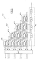
- the reference ADD designates an adder according to one embodiment of the invention. It comprises MDET determination means adapted to receive an input hold Z in at the input and two binary input numbers A and B each having in this example four bits, respectively at 0 , ... a 3 and b 0. , ... b 3 .
- the set of bits as well as the input hold Z in are delivered to MINIT initialization means.
- the MINIT initialization means initialize the signals R and U according to an algorithm described in more detail below.
- the initialisation means MINIT deliver at the output respectively the signals U 0 0, ..., U 3 0 0 and R 0, ..., R 3 0.
- the initialization means further MINIT deliver the signals U 0 -1 which initialization will be detailed in greater detail hereinafter and R 4 0 which corresponds to a first estimation of the output value of the adder ADD.
- the initialisation means MINIT are connected to a first stage of treatment MTR1 adapted to output a first bit of the estimation of the sum S, which correspond to the signals U 0 1, ..., U 3 1 and the correction signal these estimated bits of the sum, which are respectively the signals R 1 1 , ..., R 3 1 .
- the estimated bits of the sum U 0 1 , ..., U 3 1 are respectively estimated from estimation blocks BEST1, ... BEST4.
- the first stage treatment also outputs a correction signal R 4 1 of the carry output R 4 0.
- the correction signals R 1 1 ,..., R 4 1 are respectively produced using correction means, respectively MCOR1,... MCOR4.
- the first processing stage MTR1 delivers the first bit S0 of the sum S, which corresponds to the first estimate of this bit, that is to say U 0 1 .
- the MDET determination means comprise a second MTR2 processing stage. It incorporates the correction means MCOR5, MCOR6 and MCOR7 and estimation blocks BEST5, BEST6 and BEST7.
- the latter respectively deliver the correction signals R 2 2 ,..., R 4 2 and the estimated bits of the sum U 1 2 , ..., U 3 2 .
- the estimated bit U 1 2 corresponds to the second bit of the sum S1.
- Third MTR3 processing means are connected to the output of MTR2 means. These means MTR3 comprise correction blocks MCOR8 and MCOR9 and estimation means BEST8 and BEST9.
- the latter deliver the correction signals R 3 3 and R 4 3 and the estimated bits U 2 3 , which corresponds to the third bit of the sum S 2, and U 3 3 .
- the processing means are connected to the output of MTR3 processing means and comprises the correction means and the MCOR10 BEST10 estimation block, respectively delivering the correction signal R 4 4 and the estimated bit U 3 4, the latter corresponding at the last bit of the sum S3.
- Each of the correction means MCOR 1, i ranging from 1 to 10, delivering a correction signal R n j receives as input the signals U n-1 j-1 , U n-2 j-1 and the correction signal R n- 1 j-1 , n and j varying in this example from 0 to 3.
- the signal U -1 0 (defined below) is input, so as to develop the correction signal R 1 1 .
- the determination means also comprise MEL production means, comprising four means M1, M2, M3 and M4 connected in series.
- the means Mi i varying in this case from 1 to 4, receive as input the output signal of the means Mi-1 and the correction signal R 4 i .
- M1 means receive as input the first estimate of the carry output, that is to say R 4 0 issued by the initialization means MINIT.
- the means M4 output the final value of the output hold Z out .
- each estimation block BESTi incorporated in a stage of rank n, n varying from 0 to 3, and i varying from 1 to 10, comprises an "EXCLUSIVE OR" type logic gate.
- the correction means MCORi of a stage of rank n comprise a logic gate of the "EXCLUSIVE OR" type, referenced XORi, able to receive the estimated bit of the sum U n-1 j-1 and the estimated bit of the sum U n-2 j-1 .
- the MOCORi means comprise a logic gate of "ET" type, referenced ETi, and adapted to receive the output signal delivered by the logic gate XORi and the correction signal R n-1 j-1 .
- the means M1, M2, M3 M4 are each made from an "EXCLUSIVE OR" type logic gate.
- the figure 3 illustrates a first embodiment of the MINIT initialization means.
- the correction signal R 0 0 corresponds to the input hold Z in .
- variable U -1 0 is assigned here the value "0".
- the MINIT initialization means comprise four elementary initialization means ME1, ..., ME4.
- Each means MEi i varying here from 1 to 4, comprises an "EXCLUSIVE OR” type logic gate and an “AND” type logic gate respectively referenced XORii and ETii. Each of these gates respectively receives the bits of the input numbers a n-1 and b n-1 .
- Each logic gate ETii outputs the correction signal R n 0 .
- Each logic gate XORii outputs an initial value of the estimated bit U n-1 0 .
- This embodiment of the implementation of these new initialization means has the advantage of being compatible with the reversibility logic.
- the elementary initialization means MEi each comprise an inverting gate INViii, i varying from 1 to 4, capable of receiving the bit a n-1 and of delivering the initial value of the estimated bit of the sum U n. -1 0 .
- the MEi means further comprises a logic gate of the "EXCLUSIVE OR" at inverting output, referenced XORiii and receiving as input the bit a n-1 and the bit b n.
- Each logic gate XORiii outputs the correction signal R n 0 .
- the logic gate XOR444 receives in input instead of the bit of the second input number B, the binary value "0".
- the XOR444 cell is connected to the MEL generating means via another inverting gate INV5.
- the correction signal R 0 0 is delivered by a logic gate of the "EXCLUSIVE OR" type with an inverting output, referenced XOR000, receiving as input the retaining Z in and the input bit b 0 .
- the initialization variable U -1 0 is delivered by an inverting gate INV000 receiving as input the hold Z in .
- the determination means MDET comprising the initialization means represented on the FIG. figure 4 .
- the initialization values U n 0 and R n 0 are calculated according to the expressions defined above. Then a first estimate of the sum S is made by calculating the bits U n 1 . Then, the correction signals R n 1 are determined . These steps are successively repeated for the other bits of the sum S. Finally, the sum S is equal to 1000. We then find our in the case of a standard carry propagation.
- the system in question may comprise a first adder and a second adder.
- the first adder receives as input the first and second binary numbers A and B, respectively, and outputs a sum A + B.
- the second adder receives as input the intermediate sum A + B and the third binary number C and generates a sum S corresponding to the sum of the three input binary numbers A, B and C.
- the system For each additional bit number to be added, the system includes an additional adder.
- the embodiment of the MDET determination means represented on the figure 5 comprises generating means adapted to receive the signals U -1 j , U 0 j , R 0 j , ..., U 3 j , R 3 j .
- This embodiment of the MDET means is particularly suitable in the context of using an adder to perform a division.
- the generation means MGEN comprise a logic gate of "EXCLUSIVE OR" type, referenced XORiiii able to receive as input the signal U n j and the signal U n-1 j .
- the XORiiiii logic gate is connected to an "EXCLUSIVE" type logic gate with an inverting output, referenced NXORi.
- the logic gate NXORi receives as input the output signal delivered by the logic gate XORiiii and the signal R n j .
- the gate NXORi outputs the propagation signal t n j .
- the generation means MGEN are coupled to the output means for computing, so as to calculate the bits of the sum S, that is, S0, ..., S3.
- the S0 bit is then produced using an "EXCLUSIVE OR" type logic gate referenced XORS0. This receives as input the signal R 0 j and the estimated bit of the sum U 0 j .
- the S1 bit of the sum S is delivered by a logic gate of "EXCLUSIVE OR" type referenced XORS1. This receives as input the estimated bit of the sum U 1 j and the output signal of another logic gate of the type "EXCLUSIVE OR” referenced XORS12.
- the XORS12 gate receives as input the correction signal R 1 j and the output signal of a logic gate of "ET" type referenced ETS1. The latter receives as input the propagation signal t 0 j and the correction signal R 0 j .
- the S2 bit of the sum S is delivered by an XORS2 type "EXCLUSIVE OR” logic gate, which receives the estimated bit U 2 j as input and the output signal of another referenced "EXCLUSIVE OR” type logic gate.
- XORS22 The S2 bit of the sum S is delivered by an XORS2 type "EXCLUSIVE OR" logic gate, which receives the estimated bit U 2 j as input and the output signal of another referenced "EXCLUSIVE OR” type logic gate.
- the logic gate XORS22 receives as input the output signal of a logic gate of "EXCLUSIVE OR” type referenced XORS23 and the output signal of a logic gate of "ET” type referenced ETS21. The latter receives as input the propagation signal t 1 j and the correction signal R 1 j .
- the logic gate XORS23 receives as input the correction signal R 2 j and the output signal of another ETS22 type "ET" logic gate which receives as input propagation signals t 1 j and t 0 i and the signal correction number R 0 j .
- the S3 bit of the sum S is delivered by an XORS3 logic gate of the "EXCLUSIVE OR" type.
- This receives as input the estimated bit U 3 j and the output signal of another logic gate of the type "EXCLUSIVE OR" referenced XORS32.
- the logic gate XORS34 receives as input the correction signal R 3 j and the output signal of a logic gate of "ET" type referenced ETS33 which receives as input the propagation signals t 0 j , t 1 j and t 2 j and the correction signal R 0 j .
- the logic gate XORS33 referenced as input the output signals of two other doors of type "ET" respectively ETS31 and ETS32.
- the gate ETS31 receives as input the propagation signal t 2 j and the correction signal R 2 j .
- the logic gate ETS32 receives as input the propagation signals t 1 j and t 2 j and the correction signal R 1 j .
- the propagation signals produced by this type of determination means can be used within CLA type adders ("Carry-Look-Ahead" in English), to add 2n bits.
- CLA type adders Carry-Look-Ahead
- several means MDET are generated in parallel, able to generate propagation signals, in this case called group propagation signals, as well as group generation signals in the case of an addition of 2n bits as described hereinabove. after.
- the set of MDET means are combined with a so-called group propagation module well known to those skilled in the art (see for example the reference book “Advanced Computer Arithmetic Design” MJ Flynn, SF Oberman, 2001, Editions John Wiley and sons, ISBN 0-471-41209-0 pages 4 and 5).
- the group propagation module generates from the group generation signals and the group propagation signals generated by the means MDET which add the bits n, n + 1, n + 2 and n + 3 (for example), a retaining (or incoming generation term) for the MDET means that add the bits n + 4, n + 5, n + 6 and n + 7.
- the figure 6 represents means MDET used in the context of a coupling with other means MDET so as to form a type adder CLA able to add 2n bits.
- MDET means of the figure 6 are used to elaborate the terms Sn, ..., Sn + 3 of the sum S, and the so-called group generation and group propagation signals, respectively Z n + 3_i and t n + 3_i , for the module developing the term of incoming generation of the following MDET means, as explained below.
- the MGEN means of figure 6 furthermore, in comparison with the means represented on the figure 5 , a gate XORZn receiving as input the hold (incoming generation term) Zn generated by the MDET means connected upstream and the signal R j n .
- the output of the XORZn gate is connected to the gate input XORSn, ETSn + 1, ETSn + 1.2, ETSn + 3.3.
- the MGEN means comprise two logic gates XORn +3.333 and NXORn + 3, respectively of the "EXCLUSIVE OR” and "EXCLUSIVE OR” type with an inverting output.
- the gate XORn + 3,333 receives as input the signal U j n + 3 and U j n + 2 . Its output is connected to the input of the NXORn + 3 gate.
- the gate NXORn + 3 also receives the signal R j n + 3 as input and delivers another propagation signal t j n + 3 as output.
- bit Z n + 3_i is delivered by an XORZ3 logic gate of "EXCLUSIVE OR" type.
- the logic gate XORZ1 receives as input the output signals of two logic gates of type "AND" respectively referenced ETZ1 and ETZ2.
- the logic gate XORZ2 receives as input the output signals of two logic gates of type "AND" respectively referenced ETZ3 and ETZ4.
- the logic gate ETZ1 receives as input the propagation signal t n + 3 j and the correction signal R n + 3 j .
- the logic gate ETZ2 receives as input the propagation signals t n + 3 j and t n + 2 j and the correction signal R n + 2 j .
- the logic gate ETZ3 receives as input the propagation signals t n + 3 j and t n + 2 j , t n + 1 j and the correction signal R n + 1 j .
- the logic gate ETZ4 receives, as input, the propagation signals t n + 3 j t n + 2 j , t n + 1 j , t n j and the correction signal R n j .
- the MCAL means also comprise another logic gate of "ET" type, referenced ETt receiving as input the propagation signals t n + 3 j and t n + 2 j , t n + 1 j , t n j and delivering in output the signal t n + 3_i .
- figure 7 represents a multi-level adder and more precisely a 16-bit adder with group carry propagation.
- the 16-bit adder SYS comprises four blocks A 1 , A 2 , A 3 and A 4 corresponding to the means MDET as described in FIG. figure 6 .
- the first block A 1 receives as input the signals U j -1 , U j 0 , ..., U j 3 , R j 0 , ..., R j 3 and the input hold Z n (0 in this case), and outputs the first four bits of the resultant sum S 0 , .... S 3 , the generation signal per group Z 3_0 as defined in FIG. figure 6 , as well as the propagation signal by group T 3_0 (the signals U j -1 , U j 0 ,..., U j 3 , R j 0 ,..., R j 3 have been developed by means of initialization as described above, not shown here for simplification purposes).
- These signals are delivered to a group propagation module referenced MPG, which receives as input the resulting carry Z 3_0 of the first block A 1 , the group propagation signal t 3_0 and the input hold Z in .
- the MPG group propagation module elaborates the incoming generation term Z 4 of block A2.
- the blocks A 2, A 3 and A 4 respectively receive the input signals U j 4, ..., U j 7, R 4 j, ..., R j and U j 7 8 .. ., U j 11, R 8 j, ..., R j and U j 11 12, ..., U j 15, R 12 j, ..., R j 15 and the generation of terms incoming Z 4 , Z 8 and Z 12 produced by the MPG propagation module.
- the block A 2 outputs the bits S 4 , ... S 7 of the sum S
- the block A3 delivers the output bits S 8 , ..., S 11
- the block A 4 delivers the bits of the sum S 12 , ..., S 15 .
- the MPG module generates a resultant hold Z 16 , as well as a group propagation signal G 15_0 , and a group propagation signal T 15_0 .
- the signals G 15_0 and T 15_0 respectively correspond to the generation and group propagation signals of all the blocks A1,..., A4.
- the figure 8 also represents an adder with propagation of the retaining group receiving 64-bit input.
- This type of adder well known to those skilled in the art can be used with MDET means as described in the figure 5 as well as two levels of group propagation modules.
- the SYS system comprises a first level consisting of four MPG1, MPG2, MPG3 and MPG4 group propagation modules. Each group propagation module is connected to four sub-blocks, respectively A1, ..., A 4 and A 5 , ..., A 8 and A 9 , ... A 12 , and A 13 , ... , A 16 , corresponding to the MDET means represented on the figure 5 .
- the second level of group propagation module comprises an MPG5 module which receives as input the output signals delivered by each group propagation module of the first level.
- the adder as described above can be used in place of a conventional 64-bit adder, with group carry propagation in all configurations.
- the MDET means comprise MGEN generating means able to receive the signals U 1 j , U 0 j , R 0 j , ... , U 3 j , R 3 j .
- the MDET means further include MBIT means. These MBIT means perform the calculations at each bit and are attacked by the output signals of the generation means MGEN, the latter making it possible to accelerate the calculation of the output signals S0, S1, S2 and S3 and the outgoing carry-out Z out of said MBIT means.
- the signals Z 0 Z 1_0 Z and Z 2_0 3_0 are meanwhile holding signals which are transmitted between computing means MBIT.
- This simple and iterative embodiment of the MDET means is particularly compact and therefore suitable for use in an integrated circuit.
- each means MBIT of rank (n + 1) comprises a first logic gate “EXCLUSIVE OR” able to receive the retaining signal Z n-1_0 generated by the means MBIT of rank (n) and the correction signal R not j .
- the delivered signal attacks a logic AND logic gate which has for the second input the signal t not j from the MGEN means, the output of this gate "AND LOGIC" constituting the retaining signal Z n_0 propagated to the means MBIT of rank (n + 2).
- the MBIT means also comprises a second logic gate of "EXCLUSIVE OR” type receiving as a first input the signal generated by said first "EXCLUSIVE OR” gate and as a second input the signal U not j , and outputting the signal S n .
- a retaining signal Z out is generated by an "EXCLUSIVE" logic gate with an inverting output receiving as input the retaining signal Z 3_0 delivered by the means MBIT of rank 4 and the signal U 3 j .
Description
L'invention concerne les additionneurs numériques, en particulier les additionneurs formés à partir de demi-additionneurs montés en cascade.The invention relates to digital adders, in particular adders formed from cascaded half-adders.
Classiquement, pour effectuer une addition entre deux bits d'entrée, et une retenue entrante, on utilise deux demi-additionneurs montés en cascade. Le premier additionneur effectue la somme des deux bits et délivre en sortie le résultat de la somme et une première retenue intermédiaire. Le deuxième demi-additionneur reçoit en entrée la retenue entrante et le résultat de la somme obtenue précédemment et délivre en sortie, d'une part la somme de la retenue entrante et des deux bits d'entrée et d'autre part, la retenue finale.Conventionally, to perform an addition between two input bits, and an incoming retainer, two half-adders are used cascaded. The first adder performs the sum of the two bits and outputs the result of the sum and a first intermediate hold. The second half-adder receives as input the incoming carry and the result of the sum obtained previously and delivers, on the one hand, the sum of the incoming retainer and the two input bits, and on the other hand, the final hold. .
Pour effectuer la somme de deux nombres binaires de N bits chacun, on peut utiliser ce couple de demi-additionneurs plusieurs fois connectés en cascade, comme décrit par exemple dans l'ouvrage
Dans ce cas, chaque bit de rang n de la somme des deux nombres d'entrée est estimé et corrigé n fois par les retenues successives générées à chaque étage de demi-additionneurs.In this case, each bit of rank n of the sum of the two input numbers is estimated and corrected n times by the successive deductions generated at each half-adders stage.
Cependant, ce type d'additionneur ne permet d'effectuer des corrections qu'avec des retenues positives.However, this type of adder makes it possible to make corrections only with positive restraints.
En outre, l'estimation initiale des bits de la somme et des retenues dans les additionneurs standards, est incompatible avec les contraintes de la logique réversible, c'est-à-dire la possibilité à partir d'un signal de sortie de retrouver le signal d'entrée.In addition, the initial estimation of the bits of the sum and the holds in the standard adders is incompatible with the constraints of the reversible logic, that is to say the possibility from an output signal to recover the input signal.
Par ailleurs, ce type d'additionneur standard nécessite de propager chaque retenue générée à chaque étage de traitement, ce qui peut être inutile pour certaines applications, par exemple dans le cas de l'utilisation de demi-additionneurs pour effectuer des divisions.Furthermore, this type of standard adder requires propagating each retaining generated at each processing stage, which may be unnecessary for some applications, for example in the case of the use of half-adders to perform divisions.
Le document
L'invention vise à apporter une solution à ces problèmes.The invention aims to provide a solution to these problems.
A cet effet, selon un premier aspect de l'invention, il est proposé un procédé d'addition de signaux d'entrée selon la revendication 1.For this purpose, according to a first aspect of the invention, there is provided a method of adding input signals according to
En d'autres termes, on effectue successivement plusieurs estimations (j) de chaque bit de la somme des signaux d'entrée.In other words, several estimates (j) of each bit of the sum of the input signals are successively performed.
Après chaque estimation, on apporte une correction au bit de la somme estimé, puis une nouvelle estimation est effectuée à partir de la précédente estimation corrigée de ce même bit.After each estimate, a correction is made to the bit of the estimated sum, then a new estimate is made from the previous corrected estimate of the same bit.
En d'autres termes on corrige lesdites estimations (Uj ) à l'aide d'un signal de correction (Rj ) après chaque estimation, chaque bit de correction de rang (n) ![]()
![]()
![]()
![]()
![]()
![]()
![]()
![]()
Ce procédé a pour avantage de pouvoir effectuer des corrections soit négatives, soit positives à chaque estimation des bits de la somme. Les processus utilisant des additions/soustractions de manière itératives en sont améliorés.This method has the advantage of being able to make corrections either negative or positive at each estimate of the bits of the sum. Processes using iterative additions / subtractions are improved.
Les signaux d'entrée peuvent comprendre en outre une retenue d'entrée.The input signals may further include an input retainer.
De préférence, le procédé comprend outre une étape d'initialisation où on initialise la valeur des bits estimés de ladite somme et la valeur des signaux de correction, et j étapes successives de traitement, j étant un entier inférieur ou égal à N, où au cours de la kième étape, k variant de 1 à j, on estime les bits de la somme dont le rang n est compris entre k et N, et on élabore pour chaque bit de rang n, le nième signal de correction, chaque bit estimé de la somme de rang n, étant estimé à partir du bit estimé de la somme de rang n et du nième signal de correction, respectivement estimé et élaboré au cours de l'étape précédente, le nième signal de correction, étant élaboré à partir des bits estimés de la somme de rang n-1 et de rang n-2, et du (n-1)ième du signal de correction, respectivement estimés et élaboré au cours de l'étape précédente.Preferably, the method further comprises an initialization step where the value of the estimated bits of said sum and the value of the correction signals are initialized, and j successive processing steps, j being an integer less than or equal to N, or during the k th stage, k varying from 1 to j, the bits of the sum whose rank n is between k and N are estimated, and for each bit of rank n, the n th correction signal is calculated, each estimated bit of the sum of rank n, being estimated from the estimated bit of the sum of rank n and the n th correction signal respectively estimated and elaborated during the preceding step, the n th correction signal, being developed from the estimated bits of the sum of rank n-1 and rank n-2, and the (n-1) th of the correction signal, respectively estimated and developed in the previous step.
On peut en outre élaborer une retenue de sortie à partir de l'ensemble des Nièmes signaux de correction.In addition, an output restraint can be developed from all N th correction signals.
Selon un mode de mise en oeuvre, l'initialisation de chaque bit estimé de ladite somme est fonction des bits de même rang des premier et deuxième nombres d'entrée, et l'initialisation de la valeur du signal de correction de chaque bit estimé est fonction des bits de rang précédent des premier et deuxième nombres d'entrée.According to one embodiment, the initialization of each estimated bit of said sum is a function of the bits of the same rank of the first and second input numbers, and the initialization of the value of the correction signal of each estimated bit is function of the previous rank bits of the first and second input numbers.
Dans ce cas, il vient : 
-

-

- an et bn étant les bits de rang n, respectivement des premier et deuxième nombres d'entrée.
-
-
- a n and b n being the bits of rank n, respectively of the first and second input numbers.
Selon un autre mode de mise en oeuvre, l'initialisation de chaque bit estimé de ladite somme est fonction du complémentaire du bit de même rang du premier nombre d'entrée, et l'initialisation de la valeur des signaux de correction de chaque bit estimé est fonction du bit de rang précédent du premier nombre d'entrée, et du bit de même rang du deuxième nombre d'entrée.According to another mode of implementation, the initialization of each estimated bit of said sum is a function of the complement of the bit of the same rank of the first input number, and the initialization of the value of the correction signals of each estimated bit is a function of the previous rank bit of the first input number, and the bit of the same rank of the second input number.
Dans cet autre cas, il vient : 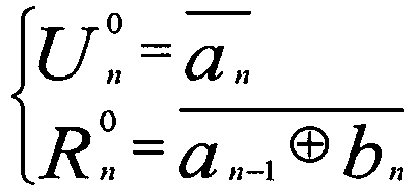
où :
-

-

- an et bn étant les bits de rang n, respectivement des premier et deuxième nombres d'entrée.
or :
-
-
- a n and b n being the bits of rank n, respectively of the first and second input numbers.
L'initialisation des signaux selon ce mode de mise en oeuvre, a pour avantage d'être compatible avec la logique de réversibilité.The initialization of the signals according to this embodiment has the advantage of being compatible with the reversibility logic.
Dans un mode de mise en oeuvre, j est égal à N, et le bit de rang n de ladite somme, correspond au bit de rang n estimé de la somme, estimé lors de la nième étape de traitement.In one embodiment, j is equal to N, and the bit of rank n of said sum, corresponds to the estimated bit of rank n of the sum, estimated during the n th processing step.
Dans un autre mode de mise en oeuvre, le procédé comprend en outre à l'issue des j étapes de traitement, une étape de génération de N-1 signaux de propagation, le qième signal de propagation étant fonction du bit estimé de ladite somme de rang q, de son signal de correction, et du bit estimé de rang q-1 de ladite somme, et dans lequel chaque bit de ladite somme est calculé à partir des qièmes signaux de propagation, tel que q est inférieur au rang du bit considéré.In another embodiment, the method further comprises, at the end of the processing steps, a step of generating N-1 propagation signals, the qth propagation signal being a function of the estimated bit of said sum. of rank q, its correction signal, and the estimated bit of rank q-1 of said sum, and wherein each bit of said sum is calculated from the qth propagation signals, such that q is less than the rank of bit considered.
Selon un autre aspect de l'invention, il est proposé un additionneur permettant d'additionner des signaux d'entrée selon la revendication 11.According to another aspect of the invention, there is provided an adder for adding input signals according to
Les signaux d'entrée peuvent comprendre en outre une retenue d'entrée.The input signals may further include an input retainer.
De préférence, l'additionneur comprend en outre des moyens d'initialisation couplés en amont des moyens de détermination, aptes à initialiser la valeur des bits estimés de ladite somme et la valeur des signaux de correction, les moyens de détermination comprenant j moyens de traitement couplés en série, j étant un entier inférieur ou égal à N, où le kième moyens de traitement, k variant de 1 à j, comportent :
- lesdits blocs d'estimation des bits de la somme dont le rang n est compris entre k et N, étant estimé à partir du bit estimé de la somme de rang n et du nième signal de correction, respectivement estimé et élaboré par les moyens de traitement connectés en amont, et
- les moyens de correction aptes à élaborer pour chaque bit de rang n, le nième signal de correction, à partir des bits estimés de la somme de rang n-1 et de rang n-2, et du (n-1)ème du signal de correction, respectivement estimés et élaboré par les moyens de traitement connectés en amont.
- said sum estimation blocks of the sum whose rank n is between k and N, being estimated from the estimated bit of the sum of rank n and the n th correction signal respectively estimated and developed by the means of upstream connected processing, and
- the correction means adapted to elaborate for each bit of rank n, the n th correction signal, from the estimated bits of the sum of rank n-1 and rank n-2, and (n-1) th of correction signal respectively estimated and developed by the processing means connected upstream.
De préférence, pour les kièmes moyens de traitement, chaque bloc d'estimation d'un bit de la somme de rang n, comprend une porte logique de type « OU EXCLUSIF » apte à recevoir en entrée le bit estimé de la somme de rang n et le nième signal de correction, respectivement estimé et élaboré par les (k-1)ièmes moyens de traitement, et dans lequel les moyens de correction d'un bit estimé de la somme de rang n+1, comprennent une autre porte logique de type « OU EXCLUSIF », apte à recevoir en entrée le bit estimé et corrigé de la somme de rang n-1, et le bit de rang (n-2) de la somme estimé et élaboré par les (k-1)ièmes moyens de traitement, et une porte logique de type « ET » couplée à la sortie de l'autre porte logique de type « OU EXCLUSIF », et apte à recevoir en entrée le signal de sortie de ladite autre porte logique et le (n-1)ème signal de correction estimé et élaboré par les (k-1)ièmes moyens de traitement.Preferably, for the k th processing means, each estimation block of a bit of the sum of rank n comprises a logic gate of the "EXCLUSIVE OR" adapted to receive as input the estimated bit of the sum of rank n and the n th correction signal respectively estimated and elaborated by the (k-1) th processing means, and in which the means for correcting an estimated bit of the sum of rank n + 1 comprise another gate "EXCLUSIVE OR" logic, able to receive as input the estimated and corrected bit of the sum of rank n-1, and the bit of rank (n-2) of the sum estimated and elaborated by the (k-1) the second processing means, and an "AND" type logic gate coupled to the output of the other "EXCLUSIVE OR" type logic gate, and adapted to receive as input the output signal of said other logic gate and the (n -1) th estimated correction signal and produced by the (k-1) th processing means.
Les moyens de traitement peuvent comprendre en outre des moyens d'élaboration aptes à élaborer une retenue de sortie à partir de l'ensemble des Nièmes signaux de correction.The processing means may furthermore comprise processing means capable of producing an output restraint from all the N th correction signals.
De préférence, les moyens d'initialisation sont aptes à initialiser la valeur de chaque bit à estimer de ladite somme en fonction des bits de même rang des premier et deuxième nombres d'entrée, et aptes à initialiser la valeur du signal de correction de chaque bit à estimer en fonction des bits de rang précédent des premier et deuxième nombres d'entrée.Preferably, the initialization means are able to initialize the value of each bit to estimate of said sum as a function of the bits of the same rank of the first and second input numbers, and able to initialize the value of the correction signal of each bit to be estimated based on the previous rank bits of the first and second input numbers.
Selon un mode de réalisation, les moyens d'initialisation comprennent N moyens d'initialisation élémentaires, chacun étant associé à un rang donné, comprenant une porte logique de type « OU EXCLUSIF », apte à recevoir les bits du rang considéré des premier et deuxième nombres d'entrée, et apte à délivrer pour le rang considéré, la valeur initiale du bit à estimer de la somme, et une portes logique de type « ET », apte à recevoir les bits du rang considéré, des premier et deuxième nombres d'entrée, et apte à délivrer la valeur initiale du signal de correction du bit estimé de la somme, du rang suivant le rang considéré.According to one embodiment, the initialization means comprise N elementary initialization means, each being associated with a given rank, comprising an "EXCLUSIVE OR" type logic gate, able to receive the bits of the rank considered of the first and second input numbers, and able to deliver for the rank in question, the initial value of the bit to be estimated of the sum, and a logical gate of the "AND" type, able to receive the bits of the rank considered, of the first and second numbers of input, and able to output the initial value of the correction signal of the estimated bit of the sum, the rank following the row considered.
Selon un autre mode de réalisation, les moyens d'initialisation comprennent N moyens d'initialisation élémentaires, chacun étant associé à un rang donné, comprenant une portes logique inverseuse, apte à recevoir le bits du rang considéré du premier nombre d'entrée, et apte à délivrer pour le rang considéré, la valeur initiale du bit à estimer de la somme, et une porte logique de type « OU EXCLUSIF » à sortie inverseuse, apte à recevoir le bit du rang considéré du premier nombre d'entrée et le bit du rang suivant le rang considéré du deuxième nombre d'entrée, et apte à délivrer la valeur initiale du signal de correction du bit estimé de la somme, du rang suivant le rang considéré.According to another embodiment, the initialization means comprise N elementary initialization means, each associated with a given rank, comprising an inverting logic gate, able to receive the bits of the rank considered of the first input number, and capable of delivering, for the rank in question, the initial value of the bit to be estimated from the sum, and an EXCLUSIVE logic gate with an inverting output, able to receive the bit of the rank considered of the first input number and the bit of the rank following the rank considered of the second entry number, and able to deliver the initial value of the correction signal of the estimated bit of the sum, of the rank according to the rank considered.
Selon une première variante, j est égal à N, et le bit de la somme de rang n, correspond au bit de la somme de rang n estimé par les nièmes moyens de traitement.In a first embodiment, j is equal to N, and the bit of the sum of rank n, corresponds to bit of the sum of rank n estimated by the nth processing means.
Selon une deuxième variante, l'additionneur comprend en outre, des moyens de génération couplés aux jièmes moyens de traitement, aptes à générer N-1 signaux de propagation, le qième signal de propagation étant fonction du bit estimé de ladite somme de rang q, de son signal de correction, et du bit estimé de rang q-1 de ladite somme, et des moyens de calcul aptes à calculer chaque bit de ladite somme à partir des qièmes signaux de propagation, tel que q est inférieur au rang du bit considéré.In a second variant, the adder further comprises generating means coupled to the j th processing means, adapted to generate N-1 spread signals, the q th propagation signal being a function of the estimated bit of said sum of rank q, of its correction signal, and the estimated bit of rank q-1 of said sum, and calculation means able to calculate each bit of said sum from the q th propagation signals, such that q is less than the rank of the bit considered.
Dans ce cas, les moyens de génération peuvent générer un Nième signal de propagation en fonction du bit estimé de rang N, de son signal de correction et du bit estimé de rang N-1. Les moyens de calcul peuvent comprendre en outre un bloc de calcul pouvant calculer un terme de génération de groupe à partir de l'ensemble des signaux de propagation générés et de l'ensemble des signaux de correction, et un terme de propagation de groupe à partir de l'ensemble des signaux de propagation.In this case, the generation means can generate an N th propagation signal as a function of the estimated bit of rank N, its correction signal and the estimated bit of rank N-1. The calculation means may furthermore comprise a calculation block that can calculate a group generation term from the set of generated propagation signals and the set of correction signals, and a group propagation term from of all the propagation signals.
Selon un mode de réalisation, si N est pair, le bloc de calcul peut alors comprendre :
- N portes logiques de type « ET », la qième porte, q variant de 1 à N, étant apte à recevoir k signaux de propagation, k variant de 1 à q, et le kième signal de correction,
- un réseau de portes logiques de type « OU EXCLUSIF », aptes à additionner l'ensemble des termes délivrés en sortie des portes logiques de type « ET », de façon à élaborer ledit terme de génération de groupe,
- une porte logique supplémentaire de type « ET », apte à multiplier l'ensemble des signaux de propagation de façon à élaborer ledit terme de propagation de groupe.
- N logic gates of "ET" type, the qth gate, q varying from 1 to N, being able to receive k propagation signals, k varying from 1 to q, and the k th correction signal,
- a network of logic gates of "EXCLUSIVE OR" type, able to add all the terms delivered at the exit of the gates logical "AND" type, so as to develop said group generation term,
- an additional logic gate of the "AND" type, able to multiply all the propagation signals so as to develop said group propagation term.
Selon un autre aspect de l'invention, il est proposé un système comprenant un réseau d'additionneurs selon le premier aspect de l'invention.According to another aspect of the invention, there is provided a system comprising an adder network according to the first aspect of the invention.
Par exemple, le système peut comprendre un réseau d'additionneurs incorporant des additionneurs selon la première ou la deuxième variante.For example, the system may comprise an adder network incorporating adders according to the first or second variant.
Par ailleurs, si N est un multiple de 4, le système peut comprendre un réseau d'additionneurs incorporant N/4 additionneurs selon la troisième variante et les différents modes de réalisation en découlant, (et tel que les signaux d'entrée comprennent une retenue d'entrée), couplés en parallèle, chaque additionneur étant apte à additionner N/4 bits successifs du premier et du deuxième nombre binaire d'entrée. Ledit système peut comprendre en outre au moins un module de propagation par groupe (MPGi) apte à recevoir le terme de génération de groupe et le terme de propagation de groupe de chaque additionneur, et aptes à élaborer à partir du terme de génération de groupe et du terme de propagation de groupe d'un additionneur donné, une retenue pour l'additionneur additionnant les N/4 bits suivants.On the other hand, if N is a multiple of 4, the system may comprise an adder network incorporating N / 4 adders according to the third variant and the various embodiments thereof, (and such that the input signals comprise a restraint input), coupled in parallel, each adder being able to add N / 4 successive bits of the first and second input binary number. Said system may furthermore comprise at least one group propagation module (MPGi) able to receive the group generation term and the group propagation term of each adder, and able to elaborate from the group generation term and the group propagation term of a given adder, a carry for the adder adding the next N / 4 bits.
Une structure de calcul simple et itérative, peut également être obtenue en intégrant au système un deuxième réseau d'additionneurs au niveau bit dans lequel le signal de correction est propagé en cascade du module de rang (n) au module de rang (n+1) sur le modèle dit « Ripple-Carry-Adder » en langue anglo-saxonne connu de l'homme de métier.A simple and iterative calculation structure can also be obtained by integrating into the system a second bit level adder network in which the correction signal is cascaded from the rank module (n) to the rank module (n + 1). ) on the model known as "Ripple-Carry-Adder" in the Anglo-Saxon language known to those skilled in the art.
D'autres avantages et caractéristiques de l'invention apparaîtront à l'examen de la description détaillée d'un mode de mise en oeuvre du procédé et de plusieurs modes de réalisation de l'invention nullement limitatifs, et des dessins annexés sur lesquels :
- la
figure 1 illustre un mode de mise en oeuvre du procédé selon l'invention, - la
figure 2 représente un schéma fonctionnel d'un mode de réalisation d'un additionneur selon l'invention, - la
figure 3 illustre plus en détail un mode de réalisation d'un additionneur selon l'invention, - la
figure 4 illustre une variante d'un mode de réalisation d'un additionneur selon l'invention, - la
figure 5 illustre un autre mode de réalisation d'un additionneur selon l'invention, - la
figure 6 illustre un autre mode de réalisation d'un additionneur selon l'invention, - les
figures 7 et 8 illustrent des modes de réalisation d'un système d'additionneur selon l'invention. - la
figure 9 illustre un autre mode de réalisation d'un additionneur selon l'invention.
- the
figure 1 illustrates an embodiment of the method according to the invention, - the
figure 2 represents a block diagram of an embodiment of an adder according to the invention, - the
figure 3 illustrates in more detail an embodiment of an adder according to the invention, - the
figure 4 illustrates a variant of an embodiment of an adder according to the invention, - the
figure 5 illustrates another embodiment of an adder according to the invention, - the
figure 6 illustrates another embodiment of an adder according to the invention, - the
figures 7 and8 illustrate embodiments of an adder system according to the invention. - the
figure 9 illustrates another embodiment of an adder according to the invention.
On se rapporte à la
Lors d'une première étape (étape préliminaire, étape 1), on initialise différents signaux Rn-1 0, Un-1 0, mis en oeuvre pour réaliser la somme de deux nombres binaires, 2respectivement A (a0, ..., an-1) et B (b0,...bn-1) et d'une retenue éventuelle Zin. On verra ci-après plus en détail la définition des termes R et U.During a first step (preliminary step, step 1), different signals R n-1 0 , U n-1 0 are initialized, implemented to produce the sum of two binary numbers, 2 respectively A (a 0 , .. ., a n-1 ) and B (b 0 , ... b n-1 ) and a possible retention Z in . The definition of the terms R and U will be described in more detail below.
Au cours d'une étape 2, on corrige les signaux R et U précédemment calculés puis on en effectue une nouvelle estimation (étape 2 ; correction et nouvelle estimation de Rn+1 j, Un+1 j).During a
A l'issue de l'étape 2, on génère le bit de la somme des signaux d'entrée (A, B, Zin) de rang n, Sn.At the end of
Puis au cours d'une étape 3, on incrémente la valeur de i d'une unité (étape 3, i i+1), puis on réitère les étapes 2 et 3 de façon à générer l'ensemble des bits de la somme S.Then during a
Lorsque l'on a généré le dernier bit de la somme S, on calcule la retenue de sortie Zout.When the last bit of the sum S has been generated, the output hold Z out is calculated.
On se rapporte à présent à la
L'ensemble des bits ainsi que la retenue d'entrée Zin sont délivrés à des moyens d'initialisation MINIT. Les moyens d'initialisation MINIT initialisent les signaux R et U selon un algorithme décrit plus en détail ci-après.The set of bits as well as the input hold Z in are delivered to MINIT initialization means. The MINIT initialization means initialize the signals R and U according to an algorithm described in more detail below.
Par conséquent, les moyens d'initialisation MINIT délivrent en sortie respectivement les signaux U0 0, ...,U3 0 et R0 0, ..., R3 0.Therefore, the initialisation means MINIT deliver at the output respectively the signals U 0 0, ..., U 3 0 0 and R 0, ..., R 3 0.
Les moyens d'initialisation MINIT délivrent en outre les signaux U-1 0 dont l'initialisation sera détaillée plus en détail ci-après et R4 0 qui correspond à une première estimation de la valeur de sortie de l'additionneur ADD.The initialization means further MINIT deliver the signals U 0 -1 which initialization will be detailed in greater detail hereinafter and R 4 0 which corresponds to a first estimation of the output value of the adder ADD.
Les moyens d'initialisation MINIT sont connectés à un premier étage de traitement MTR1 apte à délivrer une première estimation des bits de la somme S, qui correspondent respectivement aux signaux U0 1, ..., U3 1 et des signaux de correction de ces bits estimés de la somme, qui sont respectivement les signaux R1 1, ..., R3 1.The initialisation means MINIT are connected to a first stage of treatment MTR1 adapted to output a first bit of the estimation of the sum S, which correspond to the signals U 0 1, ..., U 3 1 and the correction signal these estimated bits of the sum, which are respectively the signals R 1 1 , ..., R 3 1 .
Les bits estimés de la somme U0 1, ..., U3 1 sont respectivement estimés à partir des blocs d'estimation BEST1, ...BEST4.The estimated bits of the sum U 0 1 , ..., U 3 1 are respectively estimated from estimation blocks BEST1, ... BEST4.
Le premier étage de traitement MTR1 délivre également un signal de correction R4 1 de la retenue de sortie, R4 0.MTR1 the first stage treatment also outputs a correction signal R 4 1 of the carry output R 4 0.
Les signaux de correction R1 1, ..., R4 1 sont respectivement élaborés à l'aide des moyens de correction, respectivement MCOR1, ...MCOR4.The correction signals R 1 1 ,..., R 4 1 are respectively produced using correction means, respectively MCOR1,... MCOR4.
Dans ce mode de réalisation, le premier étage de traitement MTR1, délivre le premier bit S0 de la somme S, qui correspond à la première estimation de ce bit, c'est-à-dire U0 1.In this embodiment, the first processing stage MTR1 delivers the first bit S0 of the sum S, which corresponds to the first estimate of this bit, that is to say U 0 1 .
De même, les moyens de détermination MDET comprennent un deuxième étage de traitement MTR2. Celui-ci incorpore les moyens de correction MCOR5, MCOR6 et MCOR7 et les blocs d'estimation BEST5, BEST6 et BEST7.Similarly, the MDET determination means comprise a second MTR2 processing stage. It incorporates the correction means MCOR5, MCOR6 and MCOR7 and estimation blocks BEST5, BEST6 and BEST7.
Ces derniers délivrent respectivement les signaux de correction R2 2, ..., R4 2 et les bits estimés de la somme U1 2, ..., U3 2.The latter respectively deliver the correction signals R 2 2 ,..., R 4 2 and the estimated bits of the sum U 1 2 , ..., U 3 2 .
Le bit estimé U1 2 correspond au deuxième bit de la somme S1.The estimated bit U 1 2 corresponds to the second bit of the sum S1.
Des troisièmes moyens de traitement MTR3 sont connectés à la sortie des moyens MTR2. Ces moyens MTR3 comprennent des blocs de correction MCOR8 et MCOR9 et des moyens d'estimation BEST8 et BEST9.Third MTR3 processing means are connected to the output of MTR2 means. These means MTR3 comprise correction blocks MCOR8 and MCOR9 and estimation means BEST8 and BEST9.
De même que pour les étages précédents, ces derniers délivrent les signaux de correction R3 3 et R4 3 et les bits estimés U2 3, qui correspond au troisième bit de la somme S2, et U3 3.As for the previous stages, the latter deliver the correction signals R 3 3 and R 4 3 and the estimated bits U 2 3 , which corresponds to the third bit of the
Les moyens de traitement MTR4 sont connectés à la sortie des moyens de traitement MTR3 et comprennent les moyens de correction MCOR10 et le bloc d'estimation BEST10, délivrant respectivement le signal de correction R4 4 et le bit estimé U3 4, ce dernier correspondant au dernier bit de la somme S3.MTR4 the processing means are connected to the output of MTR3 processing means and comprises the correction means and the MCOR10 BEST10 estimation block, respectively delivering the correction signal R 4 4 and the estimated bit U 3 4, the latter corresponding at the last bit of the sum S3.
L'ensemble des blocs d'estimation BESTi, i variant de 1 à 10, forment les moyens d'estimation compris dans les moyens de détermination MDET.The set of estimation blocks BESTi, i varying from 1 to 10, form the estimation means included in the determination means MDET.
Chacun des moyens de correction MCORi, i variant de 1 à 10, délivrant un signal de correction Rn j reçoit en entrée les signaux Un-1 j-1, Un-2 j-1 et le signal de correction Rn-1 j-1, n et j variant dans cet exemple de 0 à 3.Each of the correction means
Dans le cas particulier de MCOR1, le signal U-1 0 (défini ci-après) est délivré en entrée, de façon à pouvoir élaborer le signal de correction R1 1.In the particular case of MCOR1, the signal U -1 0 (defined below) is input, so as to develop the correction signal R 1 1 .
Les moyens de détermination comprennent également des moyens d'élaboration MEL, comprenant quatre moyens M1, M2, M3 et M4 connectés en série.The determination means also comprise MEL production means, comprising four means M1, M2, M3 and M4 connected in series.
Les moyens Mi, i variant dans ce cas de 1 à 4, reçoivent en entrée le signal de sortie des moyens Mi-1 et le signal de correction R4 i.The means Mi, i varying in this case from 1 to 4, receive as input the output signal of the means Mi-1 and the correction signal R 4 i .
Les moyens M1 reçoivent en entrée la première estimation de la retenue de sortie, c'est-à-dire R4 0, délivrée par les moyens d'initialisation MINIT.M1 means receive as input the first estimate of the carry output, that is to say R 4 0 issued by the initialization means MINIT.
Les moyens M4 délivrent en sortie la valeur finale de la retenue de sortie Zout.The means M4 output the final value of the output hold Z out .
On se rapporte à présent à la
Dans ce mode de réalisation, chaque bloc d'estimation BESTi, incorporé dans un étage de rang n, n variant de 0 à 3, et i variant de 1 à 10, comprend une porte logique de type « OU EXCLUSIF ».In this embodiment, each estimation block BESTi, incorporated in a stage of rank n, n varying from 0 to 3, and i varying from 1 to 10, comprises an "EXCLUSIVE OR" type logic gate.
Les moyens de correction MCORi d'un étage de rang n comprennent une porte logique de type « OU EXCLUSIF », référencée XORi, apte à recevoir le bit estimé de la somme Un-1 j-1 et le bit estimé de la somme Un-2 j-1. En outre, les moyens MOCORi comprennent une porte logique de type « ET », référencée ETi, et apte à recevoir le signal de sortie délivré par la porte logique XORi et le signal de correction Rn-1 j-1.The correction means MCORi of a stage of rank n comprise a logic gate of the "EXCLUSIVE OR" type, referenced XORi, able to receive the estimated bit of the sum U n-1 j-1 and the estimated bit of the sum U n-2 j-1 . In addition, the MOCORi means comprise a logic gate of "ET" type, referenced ETi, and adapted to receive the output signal delivered by the logic gate XORi and the correction signal R n-1 j-1 .
Par conséquent, les bits estimés Un j et les signaux de correction Rn j sont déterminés à partir des équations suivantes dites « équations de propagation » : 
En développant les équations de propagation ci-dessus, on obtient : 
où Sn représente le bit d'indice n de la somme des nombres d'entrée A, B et de la retenue entrante Zin.By developing the propagation equations above, we obtain:
where S n is the index bit n of the sum of the input numbers A, B and the incoming hold Z in .
Les moyens M1, M2, M3 M4 sont chacun réalisés à partir d'une porte logique de type « OU EXCLUSIF ».The means M1, M2, M3 M4 are each made from an "EXCLUSIVE OR" type logic gate.
La retenue de sortie Zout peut être exprimée quant à elle selon l'expression : ![]()
![]()
La
Dans ce mode de réalisation, le signal de correction R0 0 correspond à la retenue d'entrée Zin.In this embodiment, the correction signal R 0 0 corresponds to the input hold Z in .
La variable U-1 0 est affectée ici de la valeur « 0 ».The variable U -1 0 is assigned here the value "0".
Les moyens d'initialisation MINIT comprennent quatre moyens d'initialisation élémentaire ME1, ..., ME4.The MINIT initialization means comprise four elementary initialization means ME1, ..., ME4.
Chaque moyen MEi, i variant ici de 1 à 4, comprend une porte logique de type « OU EXCLUSIF » et une porte logique de type « ET » respectivement référencées XORii et ETii. Chacune de ces portes reçoit respectivement les bits des nombres d'entrée an-1 et bn-1.Each means MEi, i varying here from 1 to 4, comprises an "EXCLUSIVE OR" type logic gate and an "AND" type logic gate respectively referenced XORii and ETii. Each of these gates respectively receives the bits of the input numbers a n-1 and b n-1 .
Chaque porte logique ETii délivre en sortie le signal de correction Rn 0.Each logic gate ETii outputs the correction signal R n 0 .
Chaque porte logique XORii délivre en sortie une valeur initiale du bit estimé Un-1 0.Each logic gate XORii outputs an initial value of the estimated bit U n-1 0 .
Par conséquent, les équations implémentées par les moyens d'initialisation dans cet exemple sont : 
On se réfère à présent à la
Ce mode de réalisation de par l'implémentation de ces nouveaux moyens d'initialisation, a pour avantage d'être compatible avec la logique de réversibilité.This embodiment of the implementation of these new initialization means has the advantage of being compatible with the reversibility logic.
Dans ce mode de réalisation, les moyens élémentaires d'initialisation MEi comprennent chacun une porte inverseuse INViii, i variant de 1 à 4, apte à recevoir le bit an-1 et à délivrer la valeur initiale du bit estimé de la somme Un-1 0.In this embodiment, the elementary initialization means MEi each comprise an inverting gate INViii, i varying from 1 to 4, capable of receiving the bit a n-1 and of delivering the initial value of the estimated bit of the sum U n. -1 0 .
Les moyens MEi comprennent également une porte logique de type « OU EXCLUSIF » à sortie inverseuse, référencée XORiii et recevant en entrée le bit an-1 et le bit bn. Chaque porte logique XORiii délivre en sortie le signal de correction Rn 0.The MEi means further comprises a logic gate of the "EXCLUSIVE OR" at inverting output, referenced XORiii and receiving as input the bit a n-1 and the bit b n. Each logic gate XORiii outputs the correction signal R n 0 .
La porte logique XOR444 reçoit en entrée à la place du bit du deuxième nombre d'entrée B, la valeur binaire « 0 ».The logic gate XOR444 receives in input instead of the bit of the second input number B, the binary value "0".
Par ailleurs, la cellule XOR444 est connectée aux moyens d'élaboration MEL par l'intermédiaire d'une autre porte inverseuse INV5.Moreover, the XOR444 cell is connected to the MEL generating means via another inverting gate INV5.
Dans ce nouveau mode de réalisation des moyens MINIT, le signal de correction R0 0 est délivré par une porte logique de type « OU EXCLUSIF » à sortie inverseuse, référencée XOR000, recevant en entrée la retenue Zin et le bit d'entrée b0.In this new embodiment of the MINIT means, the correction signal R 0 0 is delivered by a logic gate of the "EXCLUSIVE OR" type with an inverting output, referenced XOR000, receiving as input the retaining Z in and the input bit b 0 .
La variable d'initialisation U-1 0 est délivrée par une porte inverseuse INV000 recevant en entrée la retenue Zin.The initialization variable U -1 0 is delivered by an inverting gate INV000 receiving as input the hold Z in .
Par conséquent, les termes Un 0 et Rn 0, n variant de 0 à 4, sont donnés par l'équation suivante : 
où l'on impose U4 0=1.Therefore, the terms U n 0 and R n 0 , n varying from 0 to 4, are given by the following equation:
where one imposes U 4 0 = 1.
Dans ce cas, l'expression, de la retenue de sortie Zout est égale à: ![]()
![]()
Dans la tableau ci-dessous, on effectue par exemple l'addition de deux nombres binaires A = 1000 et B = 1111, avec une retenue d'entrée Zin = 1.
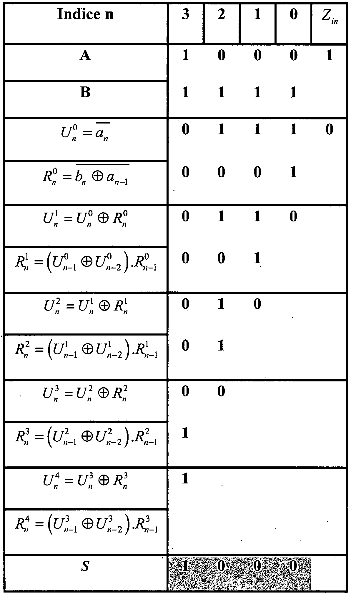
On considère dans cet exemple les moyens de détermination MDET comprenant les moyens d'initialisation représentés sur la
Au cours d'une première étape, on calcule les valeurs d'initialisation Un 0 et Rn 0 selon les expressions définies ci-avant. Puis on effectue une première estimation de la somme S en calculant les bits Un 1. Ensuite, on détermine les signaux de correction Rn 1. On répète successivement ces étapes pour les autres bits de la somme S. Finalement, la somme S est égale à 1000. On se retrouve alors dans le cas d'une propagation standard de retenue.During a first step, the initialization values U n 0 and R n 0 are calculated according to the expressions defined above. Then a first estimate of the sum S is made by calculating the bits U n 1 . Then, the correction signals R n 1 are determined . These steps are successively repeated for the other bits of the sum S. Finally, the sum S is equal to 1000. We then find ourselves in the case of a standard carry propagation.
Dans un autre exemple illustré dans le tableau ci-dessous, on additionne un nombre A égal à 0111 et un nombre B égal à 0000, la retenue d'entrée Zin étant nulle.

En répétant les mêmes opérations que celles décrite ci-avant, la somme S est égale à 0111.By repeating the same operations as those described above, the sum S is equal to 0111.
On se retrouve dans le cas d'une propagation de correction car la valeur estimée initiale 1000 est devenue après correction la valeur 0111.We find ourselves in the case of a correction propagation because the initial estimated value 1000 became after correction the value 0111.
Bien entendu, il est possible de combiner plusieurs additionneurs tels que décrits ci-avant, au sein d'un même système, pour additionner plus de deux nombres binaires.Of course, it is possible to combine several adders as described above, within the same system, to add more than two binary numbers.
Par exemple, pour additionner 3 nombre binaire, A, B et C, le système en question peut comprendre un premier additionneur et un deuxième additionneur. Le premier additionneur reçoit en entrée le premier et le deuxième nombres binaires respectivement A et B et élabore en sortie une somme A + B.For example, to add 3 binary numbers, A, B and C, the system in question may comprise a first adder and a second adder. The first adder receives as input the first and second binary numbers A and B, respectively, and outputs a sum A + B.
Le deuxième additionneur reçoit en entrée la somme intermédiaire A + B ainsi que le troisième nombre binaire C et élabore une somme S correspondant à la somme des trois nombres binaires d'entrée A, B et C.The second adder receives as input the intermediate sum A + B and the third binary number C and generates a sum S corresponding to the sum of the three input binary numbers A, B and C.
Pour chaque nombre binaire supplémentaire à additionner, le système comprend un additionneur supplémentaire.For each additional bit number to be added, the system includes an additional adder.
On se réfère à présent à la
Le mode de réalisation des moyens de détermination MDET représentés sur la
Ces signaux sont déterminés par un additionneur selon l'invention, par exemple selon l'un des modes de réalisation présentés sur les
Les signaux U-1 j, U0 j, R0 j, ..., U2 j, R2 j sont délivrés en entrée de moyens de génération MGEN qui élaborent des signaux de propagation t0 j, t1 j et t2 j, qui sont calculé à partir de l'expression : ![]()
avec n variant de 1 à 3, et j étant un entier quelconque, compris ici entre 0 et 3.The signals U -1 j , U 0 j , R 0 j , ..., U 2 j , R 2 j are delivered at the input of generation means MGEN which generates propagation signals t 0 j , t 1 j and t 2 d , which are calculated from the expression: ![]()
with n varying from 1 to 3, and j being any integer, here between 0 and 3.
Ces moyens de génération permettent d'accélérer le calcul des bits S0, S1, S2 et S3, qui sont alors obtenus par les relations ci-dessous : 
Ce mode de réalisation des moyens MDET est particulièrement adapté dans le cadre de l'utilisation d'un additionneur pour effectuer une division.This embodiment of the MDET means is particularly suitable in the context of using an adder to perform a division.
Pour l'élaboration d'un signal de propagation tn j, n variant de 0 à 2, les moyens de génération MGEN comprennent une porte logique de type « OU EXCLUSIF », référencée XORiiii apte à recevoir en entrée le signal Un j et le signal Un-1 j.For the development of a propagation signal t n j , n varying from 0 to 2, the generation means MGEN comprise a logic gate of "EXCLUSIVE OR" type, referenced XORiiii able to receive as input the signal U n j and the signal U n-1 j .
La porte logique XORiiii est connectée à une porte logique de type « OU EXCLUSIF » à sortie inverseuse, référencée NXORi. La porte logique NXORi reçoit en entrée le signal de sortie délivré par la porte logique XORiiii et le signal Rn j.The XORiiii logic gate is connected to an "EXCLUSIVE" type logic gate with an inverting output, referenced NXORi. The logic gate NXORi receives as input the output signal delivered by the logic gate XORiiii and the signal R n j .
La porte NXORi délivre en sortie le signal de propagation tn j.The gate NXORi outputs the propagation signal t n j .
Les moyens de génération MGEN sont couplés en sortie à des moyens de calcul, de manière à calculer les bits de la somme S, soit, S0, ..., S3.The generation means MGEN are coupled to the output means for computing, so as to calculate the bits of the sum S, that is, S0, ..., S3.
Le bit S0 est alors élaboré à l'aide d'une porte logique de type « OU EXCLUSIF » référencée XORS0. Celle-ci reçoit en entrée le signal R0 j et le bit estimé de la somme U0 j.The S0 bit is then produced using an "EXCLUSIVE OR" type logic gate referenced XORS0. This receives as input the signal R 0 j and the estimated bit of the sum U 0 j .
Le bit S1 de la somme S est délivré par une porte logique de type « OU EXCLUSIF » référencée XORS1. Celle-ci reçoit en entrée le bit estimé de la somme U1 j et le signal de sortie d'une autre porte logique de type « OU EXCLUSIF » référencée XORS12.The S1 bit of the sum S is delivered by a logic gate of "EXCLUSIVE OR" type referenced XORS1. This receives as input the estimated bit of the sum U 1 j and the output signal of another logic gate of the type "EXCLUSIVE OR" referenced XORS12.
La porte XORS12 reçoit en entrée le signal de correction R1 j et le signal de sortie d'une porte logique de type « ET » référencée ETS1. Cette dernière reçoit en entrée le signal de propagation t0 j et le signal de correction R0 j.The XORS12 gate receives as input the correction signal R 1 j and the output signal of a logic gate of "ET" type referenced ETS1. The latter receives as input the propagation signal t 0 j and the correction signal R 0 j .
Le bit S2 de la somme S est délivré par une porte logique de type « OU EXCLUSIF » référencée XORS2, qui reçoit en entrée le bit estimé U2 j et le signal de sortie d'une autre porte logique de type « OU EXCLUSIF » référencée XORS22.The S2 bit of the sum S is delivered by an XORS2 type "EXCLUSIVE OR" logic gate, which receives the estimated bit U 2 j as input and the output signal of another referenced "EXCLUSIVE OR" type logic gate. XORS22.
La porte logique XORS22 reçoit en entrée le signal de sortie d'une porte logique de type « OU EXCLUSIF » référencée XORS23 et le signal de sortie d'une porte logique de type « ET » référencée ETS21. Cette dernière reçoit en entrée le signal de propagation t1 j et le signal de correction R1 j.The logic gate XORS22 receives as input the output signal of a logic gate of "EXCLUSIVE OR" type referenced XORS23 and the output signal of a logic gate of "ET" type referenced ETS21. The latter receives as input the propagation signal t 1 j and the correction signal R 1 j .
La porte logique XORS23 reçoit en entrée le signal de correction R2 j et le signal de sortie d'une autre porte logique de type « ET » référencée ETS22 qui reçoit en entrée des signaux de propagation t1 j et t0 i et le signal de correction R0 j.The logic gate XORS23 receives as input the correction signal R 2 j and the output signal of another ETS22 type "ET" logic gate which receives as input propagation signals t 1 j and t 0 i and the signal correction number R 0 j .
Le bit S3 de la somme S est délivré par une porte logique XORS3 de type « OU EXCLUSIF ».The S3 bit of the sum S is delivered by an XORS3 logic gate of the "EXCLUSIVE OR" type.
Celle-ci reçoit en entrée le bit estimé U3 j et le signal de sortie d'une autre porte logique de type « OU EXCLUSIF » référencée XORS32.This receives as input the estimated bit U 3 j and the output signal of another logic gate of the type "EXCLUSIVE OR" referenced XORS32.
Celle-ci reçoit en entrée les signaux de sortie de deux autres portes logiques de type « OU EXCLUSIF » respectivement XORS34 et XORS33.The latter receives as input the output signals of two other logic gates of "EXCLUSIVE OR" type respectively XORS34 and XORS33.
La porte logique XORS34 reçoit en entrée le signal de correction R3 j et le signal de sortie d'une porte logique de type « ET » référencée ETS33 qui reçoit en entrée les signaux de propagation t0 j, t1 j et t2 j et le signal de correction R0 j.The logic gate XORS34 receives as input the correction signal R 3 j and the output signal of a logic gate of "ET" type referenced ETS33 which receives as input the propagation signals t 0 j , t 1 j and t 2 j and the correction signal R 0 j .
La porte logique référencée XORS33 reçoit en entrée les signaux de sortie de deux autres portes de type « ET » respectivement ETS31 et ETS32.The logic gate XORS33 referenced as input the output signals of two other doors of type "ET" respectively ETS31 and ETS32.
La porte ETS31 reçoit en entrée le signal de propagation t2 j et le signal de correction R2 j.The gate ETS31 receives as input the propagation signal t 2 j and the correction signal R 2 j .
La porte logique ETS32 reçoit en entrée les signaux de propagation t1 j et t2 j et le signal de correction R1 j.The logic gate ETS32 receives as input the propagation signals t 1 j and t 2 j and the correction signal R 1 j .
Les signaux de propagation élaborés par ce type de moyens de détermination peuvent être utilisés au sein des additionneurs de type CLA (« Carry-Look-Ahead » en langue anglaise), pour additionner 2n bits. Pour ce faire on couple en parallèle plusieurs moyens MDET aptes à générer des signaux de propagation, appelés dans ce cas signaux de propagation de groupe, ainsi que des signaux de génération de groupe dans le cas d'une addition de 2n bits comme décrit ci-après.The propagation signals produced by this type of determination means can be used within CLA type adders ("Carry-Look-Ahead" in English), to add 2n bits. To do this, several means MDET are generated in parallel, able to generate propagation signals, in this case called group propagation signals, as well as group generation signals in the case of an addition of 2n bits as described hereinabove. after.
L'ensemble des moyens MDET sont combinés à un module dit de propagation par groupe bien connu de l'homme du métier (voir par exemple l'ouvrage de référence « Advanced Computer Arithmetic Design» M.J. Flynn, S.F. Oberman, 2001, Editions John Wiley and sons, ISBN 0-471-41209-0 pages 4 et 5). Le module de propagation par groupe élabore à partir des signaux de génération de groupe et des signaux de propagation de groupe générés par les moyens MDET qui additionnent les bits n, n+1, n+2 et n+3 (par exemple), une retenue (ou terme de génération entrant) pour les moyens MDET qui additionnent les bits n+4, n+5, n+6 et n+7.The set of MDET means are combined with a so-called group propagation module well known to those skilled in the art (see for example the reference book "Advanced Computer Arithmetic Design" MJ Flynn, SF Oberman, 2001, Editions John Wiley and sons, ISBN 0-471-41209-0
La
Les moyens MDET de la
Les moyens MGEN de la
De plus les moyens MGEN comprennent deux portes logiques XORn+3,333 et NXORn+3 respectivement de type « OU EXCLUSIF » et « OU EXCLUSIF à sortie inverseuse ».In addition, the MGEN means comprise two logic gates XORn +3.333 and NXORn + 3, respectively of the "EXCLUSIVE OR" and "EXCLUSIVE OR" type with an inverting output.
La porte XORn+3,333 reçoit en entrée le signal Uj n+3 et Uj n+2. Sa sortie est connectée en entrée de la porte NXORn+3.The gate XORn + 3,333 receives as input the signal U j n + 3 and U j n + 2 . Its output is connected to the input of the NXORn + 3 gate.
La porte NXORn+3 reçoit également en entrée le signal Rj n+3 et délivre en sortie un autre signal de propagation tj n+3.The gate NXORn + 3 also receives the signal R j n + 3 as input and delivers another propagation signal t j n + 3 as output.
Par ailleurs, le bit Zn+3_i est délivré par une porte logique XORZ3 de type « OU EXCLUSIF ».Furthermore, the bit Z n + 3_i is delivered by an XORZ3 logic gate of "EXCLUSIVE OR" type.
Celle-ci reçoit en entrée les signaux de sortie de deux autres portes logiques de type « OU EXCLUSIF » respectivement référencée XORZ1 et XORZ2.The latter receives as input the output signals of two other logic gates of "EXCLUSIVE OR" type respectively referenced XORZ1 and XORZ2.
La porte logique XORZ1 reçoit en entrée les signaux de sortie de deux portes logiques de type « ET » respectivement référencées ETZ1 et ETZ2.The logic gate XORZ1 receives as input the output signals of two logic gates of type "AND" respectively referenced ETZ1 and ETZ2.
La porte logique XORZ2 reçoit en entrée les signaux de sortie de deux portes logiques de type « ET » respectivement référencées ETZ3 et ETZ4.The logic gate XORZ2 receives as input the output signals of two logic gates of type "AND" respectively referenced ETZ3 and ETZ4.
La porte logique ETZ1 reçoit en entrée le signal de propagation tn+3 j et le signal de correction Rn+3 j.The logic gate ETZ1 receives as input the propagation signal t n + 3 j and the correction signal R n + 3 j .
La porte logique ETZ2 reçoit en entrée les signaux de propagation tn+3 j et tn+2 j et le signal de correction Rn+2 j.The logic gate ETZ2 receives as input the propagation signals t n + 3 j and t n + 2 j and the correction signal R n + 2 j .
La porte logique ETZ3 reçoit en entrée les signaux de propagation tn+3 j et tn+2 j, tn+1 j et le signal de correction Rn+1 j.The logic gate ETZ3 receives as input the propagation signals t n + 3 j and t n + 2 j , t n + 1 j and the correction signal R n + 1 j .
La porte logique ETZ4 reçoit en entrée les signaux de propagation tn+3 j tn+2 j, tn+1 j, tn j et le signal de correction Rn j.The logic gate ETZ4 receives, as input, the propagation signals t n + 3 j t n + 2 j , t n + 1 j , t n j and the correction signal R n j .
Enfin, les moyens MCAL comprennent également une autre porte logique de type « ET », référencée ETt recevant en entrée les signaux de propagation tn+3 j et tn+2 j, tn+1 j, tn j et délivrant en sortie le signal tn+3_i.Finally, the MCAL means also comprise another logic gate of "ET" type, referenced ETt receiving as input the propagation signals t n + 3 j and t n + 2 j , t n + 1 j , t n j and delivering in output the signal t n + 3_i .
Les termes de la somme S et les signaux Zn+3_i et tn+3_i sont donc générés selon les équations suivantes : 
avec 
with
On se réfère à présent à la
Ce type d'additionneur, réalisé de façon classique, est bien connu de l'homme du métier.This type of adder, produced in a conventional manner, is well known to those skilled in the art.
L'additionneur 16 bits SYS comprend quatre blocs A1, A2, A3 et A4 correspondant aux moyens MDET tels que décrits sur la
Le premier bloc A1 reçoit en entrée les signaux Uj -1, Uj 0, ..., Uj 3, Rj 0, ..., Rj 3 et la retenue d'entrée Zn (0 dans ce cas), et délivre en sortie les quatre premiers bits de la somme résultante S0, ....S3, le signal de génération par groupe Z3_0 telle que définie dans la
Ces signaux sont délivrés à un module de propagation par groupe référencé MPG, qui reçoit en entrée la retenue résultante Z3_0 du premier bloc A1, le signal de propagation par groupe t3_0 et la retenue d'entrée Zin.These signals are delivered to a group propagation module referenced MPG, which receives as input the resulting carry Z 3_0 of the first block A 1 , the group propagation signal t 3_0 and the input hold Z in .
Le module de propagation par groupe MPG élabore le terme de génération entrant Z4 du bloc A2.The MPG group propagation module elaborates the incoming generation term Z 4 of block A2.
De même, les blocs A2, A3 et A4 reçoivent respectivement les signaux d'entrée Uj 4, ..., Uj 7, Rj 4, ..., Rj 7 et Uj 8, ..., Uj 11, Rj 8, ..., Rj 11 et Uj 12, ..., Uj 15, Rj 12, ..., Rj 15, ainsi que les termes de génération entrant Z4, Z8 et Z12 élaborés par le module de propagation MPG.Similarly, the blocks A 2, A 3 and A 4 respectively receive the input signals U j 4, ..., U j 7, R 4 j, ..., R j and U j 7 8 .. ., U j 11, R 8 j, ..., R j and U j 11 12, ..., U j 15, R 12 j, ..., R j 15 and the generation of terms incoming Z 4 , Z 8 and Z 12 produced by the MPG propagation module.
Le bloc A2 délivre en sortie les bits S4, ... S7 de la somme S, le bloc A3 délivre les bits de sortie S8, ..., S11 et le bloc A4 délivre les bits de la somme S12, ..., S15.The block A 2 outputs the bits S 4 , ... S 7 of the sum S, the block A3 delivers the output bits S 8 , ..., S 11 and the block A 4 delivers the bits of the sum S 12 , ..., S 15 .
Le terme S4 est établi grâce à la relation suivante : ![]()
avec : ![]()
![]()
with: ![]()
De même, on a: ![]()
avec : ![]()
S 16 est obtenu de la même façon.Similarly, we have: ![]()
with: ![]()
Le module MPG génère une retenue résultante Z16, ainsi qu'un signal de propagation par groupe G15_0,et un signal de propagation par groupe T15_0.The MPG module generates a resultant hold Z 16 , as well as a group propagation signal G 15_0 , and a group propagation signal T 15_0 .
Les signaux G15_0 et T15_0 correspondent respectivement aux signaux de génération et de propagation par groupe de l'ensemble des blocs A1,..., A4.The signals G 15_0 and T 15_0 respectively correspond to the generation and group propagation signals of all the blocks A1,..., A4.
La
Le système SYS comprend un premier niveau constitué de quatre modules de propagation par groupe MPG1, MPG2, MPG3 et MPG4. Chaque module de propagation par groupe est connecté à quatre sous-blocs, respectivement A1, ..., A4 et A5, ..., A8 et A9, ...A12, et A13, ..., A16, correspondant aux moyens MDET représentés sur la
Le deuxième niveau de module de propagation par groupe comprend un module MPG5 qui reçoit en entrée les signaux de sortie délivrés par chaque module de propagation par groupe du premier niveau.The second level of group propagation module comprises an MPG5 module which receives as input the output signals delivered by each group propagation module of the first level.
L'additionneur tel que décrit ci-avant peut être utilisé à la place d'un additionneur classique 64 bits, avec propagation de retenue par groupe dans toutes les configurations.The adder as described above can be used in place of a conventional 64-bit adder, with group carry propagation in all configurations.
On va maintenant décrire un autre mode de réalisation des moyens de détermination MDET en référence à la
Les moyens MDET comprennent des moyens de génération MGEN aptes à recevoir les signaux ![]()
![]()
Ceux ci sont déterminés par un additionneur selon l'invention, par exemple selon l'un des modes de réalisation présentés sur les
Les signaux ![]()
![]()
![]()
![]()
![]()
avec n variant de 1 à 3, et j étant un entier quelconque, compris ici entre 0 et 3.Signals ![]()
![]()
![]()
![]()
![]()
with n varying from 1 to 3, and j being any integer, here between 0 and 3.
Les moyens MDET comprennent de plus des moyens MBIT. Ces moyens MBIT réalisent les calculs au niveau de chaque bit et sont attaqués par les signaux de sortie des moyens de génération MGEN, ces derniers permettant d'accélérer le calcul des signaux de sortie S0, S1, S2 et S3 et de la retenue sortante Zout issue desdits moyens MBIT.The MDET means further include MBIT means. These MBIT means perform the calculations at each bit and are attacked by the output signals of the generation means MGEN, the latter making it possible to accelerate the calculation of the output signals S0, S1, S2 and S3 and the outgoing carry-out Z out of said MBIT means.
Les signaux de sortie des moyens MBIT sont obtenus par les relations ci-dessous : 
Avec : 
With:
Les signaux Z0' Z1_0' Z2_0 et Z3_0 sont quant à eux des signaux de retenue qui sont transmis entre moyens de calcul MBIT.The signals Z 0 Z 1_0 Z and Z 2_0 3_0 are meanwhile holding signals which are transmitted between computing means MBIT.
Ce mode de réalisation simple et itératif des moyens MDET est particulièrement compact et donc adapté pour une utilisation dans un circuit intégré.This simple and iterative embodiment of the MDET means is particularly compact and therefore suitable for use in an integrated circuit.
Dans la ![]()
![]()
![]()
![]()
![]()
![]()
![]()
![]()
L'homme du métier saura généraliser l'ensemble des modes de réalisation décrits ci-avant pour un nombre de bits quelconque des nombres d'entrée.Those skilled in the art will be able to generalize all the embodiments described above for any number of bits of the input numbers.
Claims (28)
- Method for additing input signals by a digital adder, the input signals comprising a first and a second binary input number, each of N bits, wherein the adder determines the bits of the sum (Sn) of the input signals (A, B) by making j estimations (Uk) of each bit of said sum, j being an integer less than or equal to N, and by correcting said estimations (Uk) with the aid of a correction signal (Rk) after each estimation,
characterised in that each correction bit of rank


a correction signal of rank n

for k ranging from 1 to j and n ranging from k to N,
and in that the estimated bits and the correction signals are output by logic gates of "EXCLUSIVE OR" type and of "AND" type. - Method according to the preceding claim, in which the input signals include, in addition, an input carry (Zin).
- Method according to one of the preceding claims, further including an initialisation step (step 1) in which the value of the estimated bits of said sum and the value of the correction signals are initialised.
- Method according to one of the preceding claims, in which an output carry (Zout) is created from the totality of the Nth correction signals.
- Method according to one of claims 3 to 4, in which the initialisation of each estimated bit of said sum is a function of the bits of identical rank of the first and second input numbers (A, B), and the initialisation of the value of the correction signal of each estimated bit is a function of the bits of preceding rank of the first and second input numbers.
- Method according to the preceding claim, in which:

where:
 an and bn being the bits of rank n of the first and second input numbers, respectively.
 - Method according to one of claims 3 to 4, in which the initialisation of each estimated bit of said sum is a function of the complement of the bit of identical rank of the first input number, and the initialisation of the value of the correction signals of each estimated bit is a function of the bit of preceding rank of the first input number and of the bit of identical rank of the second input number.
- Method according to the preceding claim, in which:

where:
 an and bn being the bits of rank n of the first and second input numbers, respectively.
 - Method according to one of the claims 3 to 8, in which j is equal to N, and in which the bit of rank n of the sum (Sn) corresponds to the estimated bit of rank n of the sum, estimated at the time of the (n+1)th processing step

- Method according to one of Claims 3 to 8, further including at the conclusion of the j processing steps, a step of generation of N-1 propagation signals

- Adder for additing input signals comprising a first (A) and a second (B) binary input number, each of N bits, to be added, characterised in that said adder includes determination means (MDET) capable of determining the bits of the sum of the input signals, comprising:- estimation means comprising estimation units (BESTi) connected in series, each estimation unit being capable of making an estimation of a bit of said sum,
an estimation of rank
 - correction means (MCORi) capable of creating a signal for correction of a bit of said sum,and in that said estimation means and correction means include logic gates of "EXCLUSIVE OR" type and of "AND" type.
a correction signal of rank

for k ranging from 1 to j, and n ranging from k to N, so as to correct each estimated bit of said sum after each estimation, each signal for correction of an estimated bit of rank n of the sum being created with the aid of the last estimated and corrected bit of rank n-1 of the sum, the signal for correction of the last bit of rank n-1, and the last estimated and corrected bit of rank n-2 of the sum, - Adder according to the preceding claim, in which the input signals include, in addition, an input carry (Zin).
- Adder according to one of the claims 11 to 12, including, in addition, initialisation means (MINIT) coupled upstream of the determination means and capable of initialising the value of the estimated bits of said sum and the value of the correction signals.
- Adder according to the preceding claim, in which for the kth processing means each unit for estimation of a bit of the sum of rank n includes a logic gate of "EXCLUSIVE OR" type, capable of receiving at its input the estimated bit of the sum of rank n and the nth correction signal, respectively estimated and created by the (k-1)th processing means, and in which the means for correction of an estimated bit of the sum of rank n+1 include another logic gate of "EXCLUSIVE OR" type, capable of receiving at its input the estimated and corrected bit of the sum of rank n-1 and the bit of rank n-2 of the sum, estimated and created by the (k-1)th processing means, and a logic gate of "AND" type, coupled to the output of the other logic gate of "EXCLUSIVE OR" type and capable of receiving at its input the output signal of said other logic gate and the (n-1)th correction signal estimated and created by the (k-1)th processing means.
- Adder according to one of claims 12 to 14, in which the processing means include, in addition, creation means (MEL) capable of creating an output carry (Zout) from the totality of the Nth correction signals.
- Adder according to one of claims 13, 14 and 15 depending on 13, in which the initialisation means (MINIT) are capable of initialising the value of each bit to be estimated of said sum as a function of the bits of identical rank of the first and second input numbers, and are capable of initialising the value of the signal for correction of each bit to be estimated as a function of the bits of preceding rank of the first and second input numbers.
- Adder according to the preceding claim, in which the initialisation means (MINIT) comprise N elementary initialisation means (MEi), each one being associated with a given rank, including a logic gate of "EXCLUSIVE OR" type, capable of receiving the bits of the rank being considered of the first and second input numbers, and capable of outputting, for the rank being considered, the initial value of the bit to be estimated of the sum, and a logic gate of "AND" type, capable of receiving the bits of the rank being considered of the first and second input numbers, and capable of outputting the initial value of the signal for correction of the estimated bit of the sum, of the rank following the rank being considered.
- Adder according to claim 16, in which the initialisation means (MINIT) comprise N elementary initialisation means (MEi), each one being associated with a given rank, including an inverting logic gate capable of receiving the bits of the rank being considered of the first input number, and capable of outputting, for the rank being considered, the initial value of the bit to be estimated of the sum, and a logic gate of "EXCLUSIVE OR" type with inverting output, capable of receiving the bit of the rank being considered of the first input number and the bit of rank following the rank being considered of the second input number, and capable of outputting the initial value of the correction signal of the estimated bit of the sum, of the rank following the rank being considered.
- Adder according to one of claims 13 to 18, in which j is equal to N, and in which the bit of the sum of rank n corresponds to the bit of the sum of rank n estimated by the (n+1)th processing means.
- Adder according to one of claims 13 to 18, including, in addition, generation means (MGEN) coupled to the jth processing means and capable of generating N-1 propagation signals, the qth propagation signal being a function of the estimated bit of said sum of rank q, of its correction signal, and of the estimated bit of rank q-1 of said sum, and calculation means (MCAL) capable of calculating each bit of said sum from the qth propagation signals, such that q is less than the rank of the bit being considered.
- Adder according to claim 20, in which the generation means (MGEN) are capable of generating an Nth propagation signal as a function of the estimated bit of rank N, of its correction signal and of the estimated bit of rank N-1, and in which the calculation means include, in addition, a calculation unit capable of calculating a group-generation term from the totality of the generated propagation signals and from the totality of the correction signals, and a group-propagation term from the set of the propagation signals.
- Adder according to the preceding claim, in which N is even, and in which the calculation unit comprises:- N logic gates of "AND" type, the qth gate, q ranging from 1 to N, being capable of receiving k propagation signals, k ranging from 1 to q, and the kth correction signal,- a network of logic gates of "EXCLUSIVE OR" type, capable of adding the totality of the terms output at the output of the logic gates of "AND" type so as to create said group-generation term,- an additional logic gate of "AND" type, capable of multiplying the totality of the propagation signals so as to create said group-propagation term.
- Adder according to one of claims 13 to 18, characterised in that the means MDET include generation means MGEN capable of receiving the signals


- Adder according to Claim 23, characterised in that the propagation signals


with n ranging from 1 to 3, and j being any integer between 0 and 3. - Adder according to Claim 24, characterised in that the output signals S0, S1, S2, S3 are obtained by the relationships:

with:
- Adder according to claim 23, characterised in that each means MBIT of rank n+1 includes a first "EXCLUSIVE OR" logic gate capable of receiving the carry signal Zn-1_0 generated by the means MBIT of rank n and the correction signal


- System comprising a network of adders according to one of claims 11 to 20.
- System according to claim 27, in which N is a multiple of 4, in which the network of adders incorporates N/4 adders (Ai) according to the combination of claim 12 and one of claims 21 to 22, coupled in parallel, each adder being capable of adding N/4 successive bits of the first and of the second binary input number, said system including, in addition, at least one group-propagation module (MPGi) capable of receiving the group-generation term and the group-propagation term of each adder, and capable of creating, from the group-generation term and from the group-propagation term of a given adder, a carry for the adder adding the following N/4 bits.
Applications Claiming Priority (2)
| Application Number | Priority Date | Filing Date | Title |
|---|---|---|---|
| FR0603549A FR2900252B1 (en) | 2006-04-21 | 2006-04-21 | N BITS ADDITER AND CORRESPONDING ADDITION METHOD. |
| PCT/FR2007/000655 WO2007122319A1 (en) | 2006-04-21 | 2007-04-19 | N-bit adder and corresponding addition method |
Publications (2)
| Publication Number | Publication Date |
|---|---|
| EP2013705A1 EP2013705A1 (en) | 2009-01-14 |
| EP2013705B1 true EP2013705B1 (en) | 2015-11-11 |
Family
ID=37680666
Family Applications (1)
| Application Number | Title | Priority Date | Filing Date |
|---|---|---|---|
| EP07731319.5A Expired - Fee Related EP2013705B1 (en) | 2006-04-21 | 2007-04-19 | N-bit adder and corresponding addition method |
Country Status (5)
| Country | Link |
|---|---|
| US (1) | US20090204659A1 (en) |
| EP (1) | EP2013705B1 (en) |
| JP (1) | JP2009534729A (en) |
| FR (1) | FR2900252B1 (en) |
| WO (1) | WO2007122319A1 (en) |
Families Citing this family (3)
| Publication number | Priority date | Publication date | Assignee | Title |
|---|---|---|---|---|
| FR2929726B1 (en) * | 2008-04-02 | 2020-11-06 | S A R L Daniel Torno | MULTI-OPERAND ADDITION PROCESS, CORRESPONDING ADDITIONER AND COMPUTER PROGRAM PRODUCT. |
| CN106528045B (en) * | 2016-11-11 | 2018-12-04 | 重庆邮电大学 | A kind of reversible plus/minus musical instruments used in a Buddhist or Taoist mass in 4 based on reversible logic gate |
| WO2023220537A1 (en) * | 2022-05-11 | 2023-11-16 | Juan Pablo Ramirez | Simple and linear fast adder |
Family Cites Families (7)
| Publication number | Priority date | Publication date | Assignee | Title |
|---|---|---|---|---|
| GB1145676A (en) * | 1966-09-28 | 1969-03-19 | Nippon Electric Co | High speed adder circuit |
| GB8326690D0 (en) * | 1983-10-05 | 1983-11-09 | Secr Defence | Digital data processor |
| JPH09231055A (en) * | 1996-02-27 | 1997-09-05 | Denso Corp | Logical operation circuit and carry look-ahead adder |
| JP3322155B2 (en) * | 1997-03-05 | 2002-09-09 | 日本電気株式会社 | Data playback device |
| US6298367B1 (en) * | 1998-04-06 | 2001-10-02 | Advanced Micro Devices, Inc. | Floating point addition pipeline including extreme value, comparison and accumulate functions |
| GB9817899D0 (en) * | 1998-08-17 | 1998-10-14 | Sgs Thomson Microelectronics | Designing addition circuits |
| WO2002008885A1 (en) * | 2000-07-21 | 2002-01-31 | Xebeo Communications, Inc. | HIGH-SPEED PARALLEL-PREFIX MODULO 2n-1 ADDERS |
-
2006
- 2006-04-21 FR FR0603549A patent/FR2900252B1/en active Active
-
2007
- 2007-04-19 WO PCT/FR2007/000655 patent/WO2007122319A1/en active Application Filing
- 2007-04-19 EP EP07731319.5A patent/EP2013705B1/en not_active Expired - Fee Related
- 2007-04-19 US US12/297,796 patent/US20090204659A1/en not_active Abandoned
- 2007-04-19 JP JP2009505930A patent/JP2009534729A/en active Pending
Also Published As
| Publication number | Publication date |
|---|---|
| JP2009534729A (en) | 2009-09-24 |
| FR2900252A1 (en) | 2007-10-26 |
| EP2013705A1 (en) | 2009-01-14 |
| FR2900252B1 (en) | 2008-09-05 |
| WO2007122319A1 (en) | 2007-11-01 |
| US20090204659A1 (en) | 2009-08-13 |
Similar Documents
| Publication | Publication Date | Title |
|---|---|---|
| EP2515228B1 (en) | Montgomery multiplication method | |
| EP0712072A1 (en) | Method for the implementation of Montgomery modular reduction | |
| EP1368747B1 (en) | Method and device for reducing the time required to perform a product, multiplication and modular exponentiation calculation using the montgomery method | |
| EP0692762B1 (en) | Parallel multiplication logical circuit | |
| EP2013705B1 (en) | N-bit adder and corresponding addition method | |
| FR2853424A1 (en) | ARCHITECTURE OF COMBINED POLYNOMIAL AND NATURAL MULTIPLIERS | |
| EP0577483B1 (en) | Digital calculation method and arithmetic unit for its implementation | |
| EP0437876B1 (en) | Programmable serial multiplier | |
| FR2867580A1 (en) | MONTGOMERY MODULAR MULTIPLIER AND CORRESPONDING MULTIPLICATION METHOD | |
| WO2020012104A1 (en) | Twiddle factor generating circuit for an ntt processor | |
| FR2689989A1 (en) | Parallel calculation of an adherent bit and partial products in a floating point multiplier unit. | |
| EP0939362B1 (en) | Modular arithmetic coprocessor for fast execution of non-modular operations | |
| EP0319421B1 (en) | Binary comparator and binary number sorting operator | |
| FR2648585A1 (en) | METHOD AND DEVICE FOR RAPID MULTIPLICATION OF COMPLEMENT A 2 CODES IN A DIGITAL SIGNAL PROCESSING SYSTEM | |
| EP0476592A2 (en) | Address generator for the data storage of a processor | |
| EP0341097B1 (en) | Recursive adder to calculate the sum of two operands | |
| CN109388372B (en) | MSD (minimum-order-of-performance) multiplication calculation method of three-value optical processor based on minimum module | |
| EP1924904B1 (en) | N bit adder and corresponding adding method | |
| EP4170479A1 (en) | Integrated circuit comprising a hardware calculator and corresponding calculation method | |
| FR2809835A1 (en) | Method for adding float point operands in multiplier by using normalizing stage that may prevent execution of increment stage after normalization | |
| EP0655685B1 (en) | Parity bit calculation device associated with a sum of two numbers | |
| EP2095222A1 (en) | Method and device for multiplying binary numbers | |
| WO2009121943A1 (en) | Method of addition with multiple operands, corresponding adder and computer program product | |
| EP0718755A1 (en) | Electronic component, more particularly capable of performing a radix 4 division of two numbers | |
| FR2843507A1 (en) | Modular exponentiation method for public key cryptography applications, especially for chip card implementation, whereby the method is suitable for parallel processor use and employs multiplier and multiplicand registers |
Legal Events
| Date | Code | Title | Description |
|---|---|---|---|
| PUAI | Public reference made under article 153(3) epc to a published international application that has entered the european phase |
Free format text: ORIGINAL CODE: 0009012 |
|
| 17P | Request for examination filed |
Effective date: 20081021 |
|
| AK | Designated contracting states |
Kind code of ref document: A1 Designated state(s): AT BE BG CH CY CZ DE DK EE ES FI FR GB GR HU IE IS IT LI LT LU LV MC MT NL PL PT RO SE SI SK TR |
|
| AX | Request for extension of the european patent |
Extension state: AL BA HR MK RS |
|
| DAX | Request for extension of the european patent (deleted) | ||
| RBV | Designated contracting states (corrected) |
Designated state(s): DE GB |
|
| 17Q | First examination report despatched |
Effective date: 20100212 |
|
| RIC1 | Information provided on ipc code assigned before grant |
Ipc: G06F 7/508 20060101ALN20150325BHEP Ipc: G06F 7/506 20060101AFI20150325BHEP |
|
| GRAP | Despatch of communication of intention to grant a patent |
Free format text: ORIGINAL CODE: EPIDOSNIGR1 |
|
| INTG | Intention to grant announced |
Effective date: 20150623 |
|
| GRAS | Grant fee paid |
Free format text: ORIGINAL CODE: EPIDOSNIGR3 |
|
| GRAA | (expected) grant |
Free format text: ORIGINAL CODE: 0009210 |
|
| AK | Designated contracting states |
Kind code of ref document: B1 Designated state(s): DE GB |
|
| REG | Reference to a national code |
Ref country code: GB Ref legal event code: FG4D Free format text: NOT ENGLISH |
|
| REG | Reference to a national code |
Ref country code: DE Ref legal event code: R096 Ref document number: 602007043857 Country of ref document: DE |
|
| REG | Reference to a national code |
Ref country code: DE Ref legal event code: R097 Ref document number: 602007043857 Country of ref document: DE |
|
| PLBE | No opposition filed within time limit |
Free format text: ORIGINAL CODE: 0009261 |
|
| STAA | Information on the status of an ep patent application or granted ep patent |
Free format text: STATUS: NO OPPOSITION FILED WITHIN TIME LIMIT |
|
| 26N | No opposition filed |
Effective date: 20160812 |
|
| PGFP | Annual fee paid to national office [announced via postgrant information from national office to epo] |
Ref country code: DE Payment date: 20170425 Year of fee payment: 11 Ref country code: GB Payment date: 20170419 Year of fee payment: 11 |
|
| REG | Reference to a national code |
Ref country code: DE Ref legal event code: R119 Ref document number: 602007043857 Country of ref document: DE |
|
| GBPC | Gb: european patent ceased through non-payment of renewal fee |
Effective date: 20180419 |
|
| PG25 | Lapsed in a contracting state [announced via postgrant information from national office to epo] |
Ref country code: DE Free format text: LAPSE BECAUSE OF NON-PAYMENT OF DUE FEES Effective date: 20181101 |
|
| PG25 | Lapsed in a contracting state [announced via postgrant information from national office to epo] |
Ref country code: GB Free format text: LAPSE BECAUSE OF NON-PAYMENT OF DUE FEES Effective date: 20180419 |