EP0340972A2 - Page printer - Google Patents
Page printer Download PDFInfo
- Publication number
- EP0340972A2 EP0340972A2 EP89304245A EP89304245A EP0340972A2 EP 0340972 A2 EP0340972 A2 EP 0340972A2 EP 89304245 A EP89304245 A EP 89304245A EP 89304245 A EP89304245 A EP 89304245A EP 0340972 A2 EP0340972 A2 EP 0340972A2
- Authority
- EP
- European Patent Office
- Prior art keywords
- dma
- circuit
- interrupt
- signal
- data
- Prior art date
- Legal status (The legal status is an assumption and is not a legal conclusion. Google has not performed a legal analysis and makes no representation as to the accuracy of the status listed.)
- Withdrawn
Links
Images


Classifications
-
- G—PHYSICS
- G06—COMPUTING; CALCULATING OR COUNTING
- G06K—GRAPHICAL DATA READING; PRESENTATION OF DATA; RECORD CARRIERS; HANDLING RECORD CARRIERS
- G06K15/00—Arrangements for producing a permanent visual presentation of the output data, e.g. computer output printers
-
- G—PHYSICS
- G06—COMPUTING; CALCULATING OR COUNTING
- G06F—ELECTRIC DIGITAL DATA PROCESSING
- G06F13/00—Interconnection of, or transfer of information or other signals between, memories, input/output devices or central processing units
- G06F13/14—Handling requests for interconnection or transfer
- G06F13/20—Handling requests for interconnection or transfer for access to input/output bus
- G06F13/28—Handling requests for interconnection or transfer for access to input/output bus using burst mode transfer, e.g. direct memory access DMA, cycle steal
- G06F13/30—Handling requests for interconnection or transfer for access to input/output bus using burst mode transfer, e.g. direct memory access DMA, cycle steal with priority control
-
- G—PHYSICS
- G06—COMPUTING; CALCULATING OR COUNTING
- G06F—ELECTRIC DIGITAL DATA PROCESSING
- G06F13/00—Interconnection of, or transfer of information or other signals between, memories, input/output devices or central processing units
- G06F13/14—Handling requests for interconnection or transfer
- G06F13/20—Handling requests for interconnection or transfer for access to input/output bus
- G06F13/32—Handling requests for interconnection or transfer for access to input/output bus using combination of interrupt and burst mode transfer
- G06F13/34—Handling requests for interconnection or transfer for access to input/output bus using combination of interrupt and burst mode transfer with priority control
-
- G—PHYSICS
- G06—COMPUTING; CALCULATING OR COUNTING
- G06K—GRAPHICAL DATA READING; PRESENTATION OF DATA; RECORD CARRIERS; HANDLING RECORD CARRIERS
- G06K2215/00—Arrangements for producing a permanent visual presentation of the output data
- G06K2215/0002—Handling the output data
- G06K2215/002—Generic data access
-
- G—PHYSICS
- G06—COMPUTING; CALCULATING OR COUNTING
- G06K—GRAPHICAL DATA READING; PRESENTATION OF DATA; RECORD CARRIERS; HANDLING RECORD CARRIERS
- G06K2215/00—Arrangements for producing a permanent visual presentation of the output data
- G06K2215/0082—Architecture adapted for a particular function
Definitions
- This invention relates to a page printer, more particularly to a page printer with means for temporarily stopping direct memory access.
- Page printers such as laser printers are widely used as output devices of computers, enabling small desktop publishing systems, for example, to produce text and graphics output with high quality and variety.
- a page printer prints a page by a scanning process in which a laser beam, for example, is switched on or off for each dot on the page, the number of dots being typically 300 per inch in both the horizontal and vertical directions. The switching is performed according to data comprising at least one bit for each dot on the page.
- a page printer is controlled by a built-in microprocessor or similar central processing unit, hereinafter referred to as a CPU.
- a page printer also has various internal memories, such as a character pattern memory in which the dot patterns of characters are stored, and a frame or strip buffer memory in which the printer creates the dot pattern for an entire page, or a strip on the page. Since large amounts of dot data must be transferred between these memories, a page printer also has a direct memory access controller, hereinafter referred to as a DMAC, which is a device for transferring data to or from a memory at high speed without requiring intervention by the CPU.
- DMAC direct memory access controller
- the CPU, DMAC, and memories are interconnected by a bus over which data can be transferred a word at a time.
- a word typically comprises 8, 16, or 32 bits.
- DMA direct memory access
- the cycle-stealing mode has many disadvantages.
- a third is that when CPU processing is contingent on the completion of the current DMA transfer, the CPU cycles inserted between the DMA cycles are wasted; during them the CPU does nothing but wait for the DMA transfer to end.
- An object of the present invention is accordingly to enable DMA transfers in a page printer to be performed in burst mode, without disabling operations by the CPU.
- a page printer comprises an interface circuit for receiving data from external apparatus and generating interrupt request signals, a bus for transferring data among the interface and other circuit blocks in the printer, a character pattern memory for storing data such as character patterns, a frame buffer memory for reading and writing data, a read-out circuit for reading data from the frame buffer memory, a mechanical control circuit for receiving information from the read-out circuit and generating control signals, a printing mechanism for printing according to these control signals, a CPU for receiving interrupt request signals, processing data, and generating signals such as a DMA request signal and a DMA restart signal, a BitBlt circuit for performing DMA transfers in response to the DMA request signal, a DMA stopping circuit, disposed in the BitBlt circuit, for stopping and restarting DMA transfers in response to a DMA stop signal and the DMA restart signal, an interrupt controller for relaying interrupt request signals to the CPU, and a DMA stop signal generating circuit, disposed in the interrupt controller, for generating the DMA stop signal when certain interrupt request signals are relaye
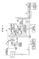
- Fig. 1 is a block diagram illustrating the structure of the novel page printer, which comprises an interface circuit 1, a bus 2, a character pattern memory 3, a frame buffer memory 4, a read-out circuit 5, a mechanical control circuit 6, a printing mechanism 7, a main controller 8, and an interrupt controller 9.
- the interface circuit 1 receives incoming data from external apparatus, temporarily stores the received data, and generates an interrupt request signal reporting the reception of a complete data byte.
- the bus 2 is a collection of signal lines interconnecting the interface circuit 1 and other circuit blocks in Fig. 1, for the interchange of information among these blocks.
- the character pattern memory 3, which is connected to the bus 2, comprises memory devices such as RAM or ROM chips storing information such as character patterns which can be placed a word at a time on the bus 2.
- the frame buffer memory 4, which is also connected to the bus 2, comprises memory devices such as RAM chips which can be written and read a word at a time via the bus 2.
- the read-out circuit 5, which is also connected to the bus 2, is a device for reading information from the frame buffer memory 4 a word at a time in synchronization with the operation of the printing mechanism 7 and transferring the information to the mechanical control circuit 6.
- the mechanical control circuit 6 monitors the status of the printing mechanism 7 and generates control signals according to this status and the information received from the read-out circuit 5.
- the printing mechanism 7, which is connected to the mechanical control circuit 6, comprises a print engine that prints characters and graphics on paper according to these control signals.
- the main controller 8 which is connected to the bus 2, is a circuit that receives interrupt request signals from the interrupt controller and performs data-processing functions such as controlling the transfer of data from the character pattern memory 3 to the frame buffer memory 4 and generating new data to be written on the frame buffer memory 4.
- the interrupt controller 9 receives interrupt request signals from the interface circuit 1 and other devices not shown in the drawing, selects among these requests according to a priority order, sends the selected interrupt request signal to the main controller, and generates DMA stop signals which it sends to the main controller 8 when certain interrupt requests are requested.
- the interface circuit 1 is a well-known circuit employing a standard interface such as the RS-232C interface or Centronics interface.
- the bus 2, character pattern memory 3, frame buffer memory 4, read-out circuit 5, mechanical control circuit 6, and printing mechanism 7 are also well-known devices, detailed descriptions of which will be omitted here.
- the external apparatus which is normally a computer, sends the page printer data indicating, for example, characters to be printed.
- the interface circuit 1 receives these data a bit or byte at a time. For each complete byte received, the interface circuit 1 sends an interrupt request signal to the interrupt controller 9, which relays it to the main controller 8.
- the main controller 8 then reads the byte of data from the interface circuit 1 and writes it in a buffer area in, for example, the frame buffer memory 4.
- the interface circuit 1 receives data at a rate of, for example, 19.2K bits per second and is capable of storing only a limited number of bytes internally: only two bytes, for example, including the byte currently being received.
- the main controller 8 must therefore read each received byte promptly, before it is lost.
- the main controller 8 processes it by calculating, for example, the address in the character pattern memory 3 at which corresponding character pattern is stored, the location at which the character should be printed on the page, and the address in the frame buffer memory 4 to which this location corresponds, then transferring the dot pattern data from the calculated address in the character pattern memory 3 to the calculated address in the frame buffer memory 4.
- the read-out circuit 5 reads them and sends them to the mechanical control circuit 6, which generates corresponding electrical signals to control the printing mechanism 7, causing the printing mechanism 7 to print the corresponding characters on the page.
- the main controller 8 comprises a CPU 15, an instruction ROM 16, and a bit block transfer circuit 17.
- a bit block transfer is commonly termed a BitBlt; this abbreviation will be employed herein.
- the CPU 15 receives the interrupt request signals received by the main controller 8. It also executes programs stored in the instruction ROM 16, which cause it to process data as already described and to generate signals, such as a DMA request signal and a DMA restart signal which it sends to the BitBlt circuit 17.
- the CPU 16 uses the bus 2 to transfer data.
- the BitBlt circuit 17 is a circuit for transferring blocks of data from the character pattern memory 3 to the frame buffer memory 4 via the bus 2, without requiring the operation of the CPU 15. Since the CPU 15 and the BitBlt circuit 17 both require the bus 2, only one of them can operate at a time.
- the CPU 15 When it becomes necessary to transfer a block of data from the character pattern memory 3 to the frame buffer memory 4, the CPU 15 first sends the BitBlt circuit 17 information indicating the location and size of the block in the character pattern memory 3 and the destination location to which it is to be transferred in the frame buffer memory 4, then sends it a DMA request signal, grants it the bus right, and halts. Upon receiving the DMA request signal and being given the bus right, the BitBlt circuit 17 begins transferring the data as requested by direct memory access.
- the BitBlt circuit 17 continues until the data transfer is completed, then returns the bus right to the CPU 15 so that the CPU 15 can resume operation. If the interrupt controller 9 generates a DMA stop signal during the data transfer, however, the BitBlt circuit 17 saves its internal status, then returns the bus right to the CPU 15 and halts.
- the interrupt controller 9 generates the DMA stop signal in conjunction with certain interrupt request signals when it sends these interrupt request signals to the CPU 15.
- the CPU 15 On receiving one of these interrupt request signals, the CPU 15 provides necessary interrupt service, which in the case of an interrupt request from the interface circuit 1 might comprise reading one byte of data from the interface circuit 1 and writing it in the frame buffer memory 4, then grants the bus right to the BitBlt circuit 17 again and sends the BitBlt circuit 17 a DMA restart signal, commanding it to resume the stopped DMA transfer.
- the BitBlt circuit 17 comprises a DMAC 18 which controls the operation of the BitBlt circuit 17, a DMA address generator 19, and a bit shifter and logic circuit 20.
- the DMAC 18 communicates with the CPU 15, from which it receives information via the bus 2 as well as via the DMA request and DMA restart signal lines.
- the DMAC 18 comprises a DMA stopping circuit 18a which enables and disables DMA operations according to the DMA restart and stop signals received from the main controller 8 and the interrupt controller 9.
- the DMA address generator 19 receives commands from the DMAC 18 and generates addresses in the character pattern memory 3 and frame buffer memory 4, causing data to be read from or written to those addresses. The data are read into or written from the bit shifter and logic circuit 20, which also performs bit shifts and other operations on these data according to commands received from the DMAC 18.
- a character pattern stored in a source block located on word boundaries in the character pattern memory 3 is transferred to a destination block located on bit boundaries in the frame buffer memory 4.
- the operation begins when the DMAC 18 receives parameters specifying the height and width of the source block and the location of the destination block from the CPU 15 via the bus 2, receives a DMA request signal, and is granted the bus right.
- the DMA address generator 19 On command from the DMAC 18, the DMA address generator 19 generates the first source address in the character pattern memory 3, the word at that address is transferred to a register in the bit shifter and logic circuit 20, the DMA address generator 19 generates the first destination address in the frame buffer memory 4, and the word at that address is transferred to another register in the bit shifter and logic circuit 20.
- the word read from character pattern memory 3 is bit-shifted to align it with the destination bit boundary and ORed with the word read from the frame buffer memory 4 to generate a result word, and the result word is written back to the same address in the frame buffer memory 4.
- the above operation is repeated a number of times equivalent to the block width, the source and destination addresses being incremented each time, to complete the transfer of one line of the block.
- the source and destination addresses are then changed to the first address in the next line of the block and that line transferred in the same way.
- the transfer of lines continues in this way for a number of times equal to the height of the block, at which point the bit block transfer is completed.
- the DMAC 18 then returns the bus right to the CPU 15.
- the DMA stopping circuit 18a halts the transfer.
- the internal status of the BitBlt circuit 17, comprising parameters such as the block height and width, the size of the bit shift, and the current source and destination addresses, is saved by remaining held in registers in the BitBlt circuit 17, these registers being static devices that do not require refreshing.
- the DMAC 18 returns the bus right to the CPU 15, which can then recommence its own operations.
- the CPU 15 When the CPU 15 is ready to allow the bit block transfer to continue, it sends a DMA restart signal to the DMA stopping circuit 18a, which causes the bit block transfer to resume from the point at which it was halted.
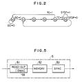
- the BitBlt circuit 17 can be embodied in a state machine with the five states illustrated in Fig. 2: an idle state S0, a source read state S1 for reading a word from the source block, a destination read state S3 for reading a word from the destination block, a bit shift state for bit-shifting the source word and ORing it with the destination word to generate a result word, a destination write state S4 for writing the result word back to the destination address, and a stop state in which the DMA transfer is stopped.
- the BitBlt circuit 17 is initially in the idle state S0.
- Transitions from the stop state S5 are controlled by a STOP signal, the BitBlt circuit 17 remaining in the stop state S5 if the STOP signal is true and returning to the source read state S2 if the STOP signal is false.
- a simple way to implement the stop state S5 is to have the STOP signal disable the state clock of the state machine.
- the STOP signal is generated by the DMA stopping circuit 18a, which can be, for example, a well-known J-K flip-flop circuit with the DMA stop signal as its J input, the DMA restart signal as its K input, and the STOP signal as its Q output.
- the STOP signal is thus originally 0, changes to 1 when a DMA stop signal is received, and changes back to 0 when a DMA restart signal is received.
- the main function of the interrupt controller 9 is to receive interrupt request signals and relay the interrupt request signal with the highest priority to the CPU 15.
- the interrupt controller 9 comprises a DMA stop signal generating circuit 91.
- the DMA stop signal generating circuit 91 also sends a DMA stop signal to the DMA stopping circuit 18a.
- Fig. 5 is a drawing illustrating an example of a circuit that can be used as the interrupt controller 9 in Fig. 1.
- the interrupt controller 9 comprises two sections: the DMA stop signal generating circuit 91, and a priority circuit 92.
- the priority circuit 92 receives four interrupt request signals IRQ1 , IRQ2 , IRQ3 , and IRQ4 , among which IRQ1 has the highest priority and IRQ4 the lowest. These signals are active low, meaning that an interrupt is requested when the corresponding signal is in the low voltage state.
- the DMA stop signal generating circuit 91 comprises inverters 93, 94, and 95, the outputs of which are opposite in level to their inputs, OR gates 96, 97, and 98, the outputs of which are high when either of their inputs is high, and a NAND gate 99, the output of which is high when either of its inputs is low.
- the inverter 93 receives IRQ1 , inverts it, and provides it as an input to the OR gates 96, 97, and 98.
- the inverter 94 receives IRQ2 , inverts it, and provides it as an input to the OR gates 97 and 98.
- the inverter 95 receives IRQ3 , inverts it, and provides it as an input to the OR gate 98.
- the outputs of the OR gates are sent as interrupt request signals IRQ1 , IRQ2 , IRQ3 , and IRQ4 to the CPU 15, these signals also being active low.
- IRQ1 and the output of the OR gate 96 are furthermore connected as inputs to the NAND gate 99.
- the output of the NAND gate 99 is the DMA stop signal, which is active high.
- This circuit operates as follows. Suppose first that IRQ1 goes low to request an interrupt.
- the interrupt request signal IRQ1 is relayed directly to the CPU 15. In addition, it is input to the NAND gate 99, the output of which therefore goes high, sending a DMA stop signal to the DMA stopping circuit 18a.
- IRQ2 goes low to request an interrupt. If IRQ1 is high, then the output of the inverter 94 is low, so both inputs to the OR gate 97 are low, hence its output is low. Thus the interrupt request IRQ2 is relayed to the CPU 15. In addition, the low output of the OR gate 97 is input to the NAND gate 99, sending a DMA stop signal to the DMA stopping circuit 18a. If IRQ1 is low when IRQ2 goes low, however, then the output of the inverter 94 is high, so the output of the OR gate 97 is high and IRQ1 is not relayed to the CPU 15 or the NAND gate 99. That is, an IRQ2 request is honored only if there is no IRQ1 request.
- an IRQ3 request is honored only if neither IRQ1 nor IRQ2 is requested, and an IRQ4 request is honored only if none of the other interrupts is requested. IRQ3 and IRQ4 do not cause output of the DMA stop signal.
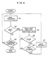
- Fig. 4 is a flowchart showing the operation of a page printer having an interrupt controller 9 like the one in Fig. 3 in which the interrupt request generated by the interface circuit 1 when a complete byte of data is received is IRQ1 , illustrating in particular the method by which a DMA transfer is halted to allow the main controller 8 to read and process the received data.
- the main controller 8 starts a DMA transfer to execute a BitBlt.
- the interrupt controller 9 tests the IRQ1 signal to see if the interface circuit 1 is requesting a data-received interrupt. If it is not, in the third step 43 the main controller 8 decides whether the DMA transfer has been completed. If the DMA transfer is not complete, the third step 43 loops back to the first step 41 to transfer another word by DMA. If the DMA transfer is complete, it ends.
- the interrupt controller 9 If the interface circuit 1 is requesting a received-data interrupt when the interrupt controller 9 tests the IRQ1 signal in the second step 42, then the interrupt controller 9 generates a DMA stop signal, stopping the DMA transfer, and the main controller 8 proceeds to the fourth step 44, in which it services the interrupt request by reading the received data from the interface circuit 1 and storing it in the frame buffer memory 4, for example, or otherwise processing the received data.
- the main controller 8 decides whether interrupt service is complete, returning to the fourth step 44 if it is not.
- the main controller 8 checks IRQ1 to decide whether the interrupt request has been cleared; that is, to see if another byte of received data requires processing. If the interrupt request is cleared, in the seventh step 47 the main controller 8 restarts the DMA transfer, returning to the first step 41.
- An advantage of the novel page printer evident from Fig. 4 is that it stops a DMA transfer only when necessary, and only for the necessary length of time. DMA transfers are completed more quickly than in the prior art because they are performed continuously, in burst mode, except when stopped. Transfer of the bus right between the CPU 15 and the DMAC 18 is held to the minimum necessary, thus saving time by reducing the number of overhead cycles.
- the novel page printer does not waste time by returning the bus right to the CPU 15 after every DMA cycle even when the CPU 15 cannot proceed with with further processing until the DMA transfer is completed. For these reasons the novel page printer is able to operate more efficiently than a prior-art page printer and print more pages per minute.
- a page printer may perform DMA transfers other than bit block transfers from the character pattern memory 3 to the frame buffer memory 4. DMA transfers may be used, for example in the read-out circuit 5 to transfer data from the frame buffer memory 4 to the mechanical control circuit 6.
- Fig. 5 shows the structure of the read-out circuit 5 in greater detail.
- the read-out circuit 5 comprises a main read-out circuit 51 for reading data from the frame buffer memory 4, a read-out buffer memory 52 in which the main read-out circuit 51 writes the data read from the frame buffer memory 4, and a synchronization circuit 53 that transfers the data from the read-out buffer memory 52 to the mechanical control circuit 6 in synchronization with the mechanical operation of the page printer.
- the main read-out circuit 51 operates under control of the CPU 15 in the main controller 8, but to reduce the load on the CPU 15, the main read-out circuit 51 transfers data by direct memory access, so that the CPU 15 need only notify it of the amount of data to be transferred and the initial transfer address. The transfer is then performed by a read-out DMAC 55 in the main read-out circuit 51 without further control by the CPU 15.
- the read-out DMAC 55 is similar in structure to the DMAC in the main controller 8, and comprises a similar DMA stopping circuit for stopping DMA transfer operations in response to a DMA stop signal from the DMA stop signal generating circuit 91.
- the read-out DMAC 55 and the DMAC 18 in the page printer can be part of the same physical unit, using the same DMAC hardware, which may serve still further DMA requests as well.
- Fig. 6 illustrates a multi-channel DMAC 60 that may be used when there are multiple DMA request signals DMAREQ1 , DMAREQ2 , DMAREQ3 , and DMAREQ4 , also showing a DMA priority circuit 66 for prioritizing the DMA requests.
- the multi- channel DMAC 60 comprises OR gates 61, 62, 63, and 64 for receiving respective DMA request signals DMAREQ1 , DMAREQ2 , DMAREQ3 , and DMAREQ4 , these signals being active low, and a J-K flip-flop 65.
- the J-K flip-flop 65 receives the DMA stop signal at its J input terminal and the DMA restart signal at its K input terminal and generates a STOP signal at its Q output terminal, which is connected to input terminals of all four of the OR gates 61, 62, 63, and 64.
- the STOP signal is thus initially low, goes high when a DMA stop signal is received, and goes low again when a DMA restart signal is received. While the STOP signal is high, the outputs of all four OR gates 61, 62, 63, and 64 are high.
- the DMA priority circuit 66 comprises inverters 67, 68, and 69 and OR gates 70, 71, and 72. These are interconnected and operate in the same way as the inverters 93, 94, and 95 and OR gates 96, 97, and 98 in Fig. 3, so further description will be omitted.
- the operation of a page printer using the multi-channel DMAC 60 is similar to that already described.
- the STOP signal in Fig. 6 is normally low, enabling the DMA request signals and allowing DMA transfers to be performed.
- the interrupt controller 9 receives an interrupt request for which the DMA transfer must be stopped, it generates a DMA stop signal which causes the STOP signal to go high. This in turn causes the outputs of all the OR gates 61, 62, 63, 64, 70, 71, and 72 in Fig. 6 to go high, disabling all of the DMA request outputs.
- the current DMA transfer operation then stops, allowing the CPU 15 to service the interrupt.
- the CPU 15 sends a DMA restart signal which resets the J-K flip-flop 65, causing the STOP signal to go low and thereby re-enabling the DMA request signals, so that the DMA transfer can resume.
- a page printer employing the multi-channel DMAC circuit in Fig. 6 efficiently performs not only bit block transfers from the character pattern memory to the frame buffer memory but a variety of other DMA transfers as well, performing all these DMA transfers in burst mode, stopping them only when necessary to allow the CPU to service an interrupt request.
- a further advantage of this invention is that the manufacture of the novel page printer does not require extensive changes changes to existing printer designs. Basically, it is only necessary to add the J-K flip-flop 65, the NAND gate 99, and OR gates such as the OR gates 61, 62, 63, and 64 to the printer hardware, and make simple modifications in the interrupt service routines stored in the instruction ROM 16 to have the CPU 15 send a DMA restart signal to the DMA stopping circuit 18a.
- the novel page printer can therefore be produced using substantially the same manufacturing facilities as in the prior art.
- Figs. 2, 3, and 6 illustrate possible structures of the DMAC, the DMA stop signal generating circuit, and the DMA stopping circuit; they do not restrict these circuits to the structures shown.
- the flowchart in Fig. 4 is also illustrative in nature, and does not show all steps that would actually be performed, such as steps for handling interrupt requests other than IRQ1 .
- the DMAC can save its internal status to a separate memory device, instead of holding it in static internal registers and restore its internal status from this separate memory device when a DMA restart signal is received; this modification enables dynamic registers to be used in the DMAC.
- the character pattern memory can store information other than character patterns, and it also possible for the character pattern memory to be partly or wholly contained within the frame buffer memory, in which case data transfers from the character pattern memory to the frame buffer memory take the form of transfers from one part of the frame buffer memory to another. It will also be apparent that the method of stopping DMA operations in this invention can be used to improve the speed of DMA transfers in devices other than page printers.
Abstract
Description
- This invention relates to a page printer, more particularly to a page printer with means for temporarily stopping direct memory access.
- Page printers such as laser printers are widely used as output devices of computers, enabling small desktop publishing systems, for example, to produce text and graphics output with high quality and variety. A page printer prints a page by a scanning process in which a laser beam, for example, is switched on or off for each dot on the page, the number of dots being typically 300 per inch in both the horizontal and vertical directions. The switching is performed according to data comprising at least one bit for each dot on the page.
- The operation of a page printer is controlled by a built-in microprocessor or similar central processing unit, hereinafter referred to as a CPU. A page printer also has various internal memories, such as a character pattern memory in which the dot patterns of characters are stored, and a frame or strip buffer memory in which the printer creates the dot pattern for an entire page, or a strip on the page. Since large amounts of dot data must be transferred between these memories, a page printer also has a direct memory access controller, hereinafter referred to as a DMAC, which is a device for transferring data to or from a memory at high speed without requiring intervention by the CPU.
- The CPU, DMAC, and memories are interconnected by a bus over which data can be transferred a word at a time. (A word typically comprises 8, 16, or 32 bits.) During a direct memory access (hereinafter DMA) operation the bus is controlled by the DMAC and cannot be used by the CPU; that is, the CPU cannot operate.
- Some scheme is necessary to ensure that the CPU will not be disabled for extended periods of time by long DMA operations, leaving it unable to deal with exigencies such as the arrival of new data from the computer. A typical scheme used in prior-art page printers is cycle stealing, in which the DMAC transfers data one word at a time, returning the bus to the CPU after each word.
- Compared with the burst mode, in which the DMAC transfers data continuously, the cycle-stealing mode has many disadvantages. One is that, since CPU cycles are interspersed between the DMA cycles, a cycle-stealing DMA transfer takes longer to complete than a burst-mode DMA transfer. Another is that extra overhead cycles are required to transfer the bus right repeatedly between the CPU and DMAC. A third is that when CPU processing is contingent on the completion of the current DMA transfer, the CPU cycles inserted between the DMA cycles are wasted; during them the CPU does nothing but wait for the DMA transfer to end.
- An object of the present invention is accordingly to enable DMA transfers in a page printer to be performed in burst mode, without disabling operations by the CPU.
- A page printer according to this invention comprises an interface circuit for receiving data from external apparatus and generating interrupt request signals, a bus for transferring data among the interface and other circuit blocks in the printer, a character pattern memory for storing data such as character patterns, a frame buffer memory for reading and writing data, a read-out circuit for reading data from the frame buffer memory, a mechanical control circuit for receiving information from the read-out circuit and generating control signals, a printing mechanism for printing according to these control signals, a CPU for receiving interrupt request signals, processing data, and generating signals such as a DMA request signal and a DMA restart signal, a BitBlt circuit for performing DMA transfers in response to the DMA request signal, a DMA stopping circuit, disposed in the BitBlt circuit, for stopping and restarting DMA transfers in response to a DMA stop signal and the DMA restart signal, an interrupt controller for relaying interrupt request signals to the CPU, and a DMA stop signal generating circuit, disposed in the interrupt controller, for generating the DMA stop signal when certain interrupt request signals are relayed to the CPU.
-
- Fig. 1 is a block diagram of a page printer according to this invention.
- Fig. 2 is a state transition diagram of a DMA controller used in the page printer in Fig. 1.
- Fig. 3 is a schematic diagram of the interrupt controller in Fig. 1.
- Fig. 4 is a flowchart illustrating the DMA stopping procedure of the page printer in Fig. 1.
- Fig. 5 is a block diagram of the read-out circuit in Fig. 1.
- Fig. 6 is a schematic diagram of a multi-channel DMA stopping circuit.
- A novel page printer according to this invention will be described with reference to the drawings.
- Fig. 1 is a block diagram illustrating the structure of the novel page printer, which comprises an
interface circuit 1, abus 2, acharacter pattern memory 3, aframe buffer memory 4, a read-out circuit 5, amechanical control circuit 6, aprinting mechanism 7, amain controller 8, and aninterrupt controller 9. Theinterface circuit 1 receives incoming data from external apparatus, temporarily stores the received data, and generates an interrupt request signal reporting the reception of a complete data byte. Thebus 2 is a collection of signal lines interconnecting theinterface circuit 1 and other circuit blocks in Fig. 1, for the interchange of information among these blocks. Thecharacter pattern memory 3, which is connected to thebus 2, comprises memory devices such as RAM or ROM chips storing information such as character patterns which can be placed a word at a time on thebus 2. Theframe buffer memory 4, which is also connected to thebus 2, comprises memory devices such as RAM chips which can be written and read a word at a time via thebus 2. The read-out circuit 5, which is also connected to thebus 2, is a device for reading information from the frame buffer memory 4 a word at a time in synchronization with the operation of theprinting mechanism 7 and transferring the information to themechanical control circuit 6. Themechanical control circuit 6 monitors the status of theprinting mechanism 7 and generates control signals according to this status and the information received from the read-out circuit 5. Theprinting mechanism 7, which is connected to themechanical control circuit 6, comprises a print engine that prints characters and graphics on paper according to these control signals. Themain controller 8, which is connected to thebus 2, is a circuit that receives interrupt request signals from the interrupt controller and performs data-processing functions such as controlling the transfer of data from thecharacter pattern memory 3 to theframe buffer memory 4 and generating new data to be written on theframe buffer memory 4. Theinterrupt controller 9 receives interrupt request signals from theinterface circuit 1 and other devices not shown in the drawing, selects among these requests according to a priority order, sends the selected interrupt request signal to the main controller, and generates DMA stop signals which it sends to themain controller 8 when certain interrupt requests are requested. - The
interface circuit 1 is a well-known circuit employing a standard interface such as the RS-232C interface or Centronics interface. Thebus 2,character pattern memory 3,frame buffer memory 4, read-out circuit 5,mechanical control circuit 6, andprinting mechanism 7 are also well-known devices, detailed descriptions of which will be omitted here. - The general operation of the novel page printer can be described as follows. The external apparatus, which is normally a computer, sends the page printer data indicating, for example, characters to be printed. The
interface circuit 1 receives these data a bit or byte at a time. For each complete byte received, theinterface circuit 1 sends an interrupt request signal to theinterrupt controller 9, which relays it to themain controller 8. Themain controller 8 then reads the byte of data from theinterface circuit 1 and writes it in a buffer area in, for example, theframe buffer memory 4. - The
interface circuit 1 receives data at a rate of, for example, 19.2K bits per second and is capable of storing only a limited number of bytes internally: only two bytes, for example, including the byte currently being received. Themain controller 8 must therefore read each received byte promptly, before it is lost. - Having read and stored a received data byte, the
main controller 8 processes it by calculating, for example, the address in thecharacter pattern memory 3 at which corresponding character pattern is stored, the location at which the character should be printed on the page, and the address in theframe buffer memory 4 to which this location corresponds, then transferring the dot pattern data from the calculated address in thecharacter pattern memory 3 to the calculated address in theframe buffer memory 4. When the dot patterns for an entire page or strip have been created in theframe buffer memory 4, the read-out circuit 5 reads them and sends them to themechanical control circuit 6, which generates corresponding electrical signals to control theprinting mechanism 7, causing theprinting mechanism 7 to print the corresponding characters on the page. - Next the structure and operation of the
main controller 8 will be described in more detail. As shown in Fig. 1, themain controller 8 comprises aCPU 15, aninstruction ROM 16, and a bitblock transfer circuit 17. (A bit block transfer is commonly termed a BitBlt; this abbreviation will be employed herein.) TheCPU 15 receives the interrupt request signals received by themain controller 8. It also executes programs stored in theinstruction ROM 16, which cause it to process data as already described and to generate signals, such as a DMA request signal and a DMA restart signal which it sends to theBitBlt circuit 17. TheCPU 16 uses thebus 2 to transfer data. The BitBltcircuit 17 is a circuit for transferring blocks of data from thecharacter pattern memory 3 to theframe buffer memory 4 via thebus 2, without requiring the operation of theCPU 15. Since theCPU 15 and the BitBltcircuit 17 both require thebus 2, only one of them can operate at a time. - Normally the
CPU 15 is active and theBitBlt circuit 17 is inactive. When it becomes necessary to transfer a block of data from thecharacter pattern memory 3 to theframe buffer memory 4, theCPU 15 first sends theBitBlt circuit 17 information indicating the location and size of the block in thecharacter pattern memory 3 and the destination location to which it is to be transferred in theframe buffer memory 4, then sends it a DMA request signal, grants it the bus right, and halts. Upon receiving the DMA request signal and being given the bus right, the BitBltcircuit 17 begins transferring the data as requested by direct memory access. If theinterrupt controller 9 does not generate a DMA stop signal during the data transfer, theBitBlt circuit 17 continues until the data transfer is completed, then returns the bus right to theCPU 15 so that theCPU 15 can resume operation. If theinterrupt controller 9 generates a DMA stop signal during the data transfer, however, theBitBlt circuit 17 saves its internal status, then returns the bus right to theCPU 15 and halts. - The
interrupt controller 9 generates the DMA stop signal in conjunction with certain interrupt request signals when it sends these interrupt request signals to theCPU 15. On receiving one of these interrupt request signals, theCPU 15 provides necessary interrupt service, which in the case of an interrupt request from theinterface circuit 1 might comprise reading one byte of data from theinterface circuit 1 and writing it in theframe buffer memory 4, then grants the bus right to the BitBltcircuit 17 again and sends the BitBlt circuit 17 a DMA restart signal, commanding it to resume the stopped DMA transfer. - Next the structure and operation of the
BitBlt circuit 17 will be described in greater detail. As shown in Fig. 1, theBitBlt circuit 17 comprises aDMAC 18 which controls the operation of theBitBlt circuit 17, aDMA address generator 19, and a bit shifter andlogic circuit 20. TheDMAC 18 communicates with theCPU 15, from which it receives information via thebus 2 as well as via the DMA request and DMA restart signal lines. TheDMAC 18 comprises aDMA stopping circuit 18a which enables and disables DMA operations according to the DMA restart and stop signals received from themain controller 8 and the interruptcontroller 9. TheDMA address generator 19 receives commands from theDMAC 18 and generates addresses in thecharacter pattern memory 3 andframe buffer memory 4, causing data to be read from or written to those addresses. The data are read into or written from the bit shifter andlogic circuit 20, which also performs bit shifts and other operations on these data according to commands received from theDMAC 18. - In the bit block transfer operation performed by the
BitBlt circuit 17, a character pattern stored in a source block located on word boundaries in thecharacter pattern memory 3 is transferred to a destination block located on bit boundaries in theframe buffer memory 4. The operation begins when theDMAC 18 receives parameters specifying the height and width of the source block and the location of the destination block from theCPU 15 via thebus 2, receives a DMA request signal, and is granted the bus right. On command from theDMAC 18, theDMA address generator 19 generates the first source address in thecharacter pattern memory 3, the word at that address is transferred to a register in the bit shifter andlogic circuit 20, theDMA address generator 19 generates the first destination address in theframe buffer memory 4, and the word at that address is transferred to another register in the bit shifter andlogic circuit 20. The word read fromcharacter pattern memory 3 is bit-shifted to align it with the destination bit boundary and ORed with the word read from theframe buffer memory 4 to generate a result word, and the result word is written back to the same address in theframe buffer memory 4. The above operation is repeated a number of times equivalent to the block width, the source and destination addresses being incremented each time, to complete the transfer of one line of the block. The source and destination addresses are then changed to the first address in the next line of the block and that line transferred in the same way. The transfer of lines continues in this way for a number of times equal to the height of the block, at which point the bit block transfer is completed. TheDMAC 18 then returns the bus right to theCPU 15. - If a DMA stop signal is received during a bit block transfer, the
DMA stopping circuit 18a halts the transfer. The internal status of theBitBlt circuit 17, comprising parameters such as the block height and width, the size of the bit shift, and the current source and destination addresses, is saved by remaining held in registers in theBitBlt circuit 17, these registers being static devices that do not require refreshing. TheDMAC 18 returns the bus right to theCPU 15, which can then recommence its own operations. When theCPU 15 is ready to allow the bit block transfer to continue, it sends a DMA restart signal to theDMA stopping circuit 18a, which causes the bit block transfer to resume from the point at which it was halted. - The
BitBlt circuit 17 can be embodied in a state machine with the five states illustrated in Fig. 2: an idle state S0, a source read state S1 for reading a word from the source block, a destination read state S3 for reading a word from the destination block, a bit shift state for bit-shifting the source word and ORing it with the destination word to generate a result word, a destination write state S4 for writing the result word back to the destination address, and a stop state in which the DMA transfer is stopped. TheBitBlt circuit 17 is initially in the idle state S0. When a G0 signal is generated, by a DMA request signal from theCPU 15 for example, a transition occurs from the idle state S0 to the source read state S1, then to the destination read state S2, then to the bit shift state S3, then to the destination write state S4. In the S4 state, after writing the destination word, theBitBlt circuit 17 checks whether the bit block transfer is complete. If it is (TC = 1), a transition occurs from the destination write state S4 to the idle state S1. If the transfer is not complete (TC = 0), a transition occurs to the stop state S5. Transitions from the stop state S5 are controlled by a STOP signal, theBitBlt circuit 17 remaining in the stop state S5 if the STOP signal is true and returning to the source read state S2 if the STOP signal is false. A simple way to implement the stop state S5 is to have the STOP signal disable the state clock of the state machine. - The STOP signal is generated by the
DMA stopping circuit 18a, which can be, for example, a well-known J-K flip-flop circuit with the DMA stop signal as its J input, the DMA restart signal as its K input, and the STOP signal as its Q output. Thus the STOP signal is thus originally 0, changes to 1 when a DMA stop signal is received, and changes back to 0 when a DMA restart signal is received. - Techniques for building state machines are well known, so a description of the structural details of Fig. 2 will be omitted.
- Next the interrupt
controller 9 in Fig. 1 will be described in more detail. The main function of the interruptcontroller 9 is to receive interrupt request signals and relay the interrupt request signal with the highest priority to theCPU 15. In addition, the interruptcontroller 9 comprises a DMA stopsignal generating circuit 91. For certain interrupts, when the interruptcontroller 9 relays the interrupt request signal to theCPU 15, the DMA stopsignal generating circuit 91 also sends a DMA stop signal to theDMA stopping circuit 18a. - Fig. 5 is a drawing illustrating an example of a circuit that can be used as the interrupt
controller 9 in Fig. 1. In this example there are four interrupt request sources, and the DMA stop signal is generated for the two interrupts with the highest priority. The interruptcontroller 9 comprises two sections: the DMA stopsignal generating circuit 91, and apriority circuit 92. Thepriority circuit 92 receives four interrupt request signalsIRQ1 ,IRQ2 ,IRQ3 , andIRQ4 , among whichIRQ1 has the highest priority andIRQ4 the lowest. These signals are active low, meaning that an interrupt is requested when the corresponding signal is in the low voltage state. The DMA stopsignal generating circuit 91 comprisesinverters gates 96, 97, and 98, the outputs of which are high when either of their inputs is high, and aNAND gate 99, the output of which is high when either of its inputs is low. Theinverter 93 receivesIRQ1 , inverts it, and provides it as an input to the ORgates 96, 97, and 98. Theinverter 94 receivesIRQ2 , inverts it, and provides it as an input to the ORgates 97 and 98. Theinverter 95 receivesIRQ3 , inverts it, and provides it as an input to the OR gate 98. The outputs of the OR gates are sent as interrupt request signalsIRQ1 ,IRQ2 ,IRQ3 , andIRQ4 to theCPU 15, these signals also being active low.IRQ1 and the output of the OR gate 96 are furthermore connected as inputs to theNAND gate 99. The output of theNAND gate 99 is the DMA stop signal, which is active high. - This circuit operates as follows. Suppose first that
IRQ1 goes low to request an interrupt. The interrupt request signalIRQ1 is relayed directly to theCPU 15. In addition, it is input to theNAND gate 99, the output of which therefore goes high, sending a DMA stop signal to theDMA stopping circuit 18a. - Suppose next that
IRQ2 goes low to request an interrupt. IfIRQ1 is high, then the output of theinverter 94 is low, so both inputs to theOR gate 97 are low, hence its output is low. Thus the interrupt requestIRQ2 is relayed to theCPU 15. In addition, the low output of theOR gate 97 is input to theNAND gate 99, sending a DMA stop signal to theDMA stopping circuit 18a. IfIRQ1 is low whenIRQ2 goes low, however, then the output of theinverter 94 is high, so the output of theOR gate 97 is high andIRQ1 is not relayed to theCPU 15 or theNAND gate 99. That is, anIRQ2 request is honored only if there is noIRQ1 request. - Similarly, an
IRQ3 request is honored only if neitherIRQ1 norIRQ2 is requested, and anIRQ4 request is honored only if none of the other interrupts is requested.IRQ3 andIRQ4 do not cause output of the DMA stop signal. - Fig. 4 is a flowchart showing the operation of a page printer having an interrupt
controller 9 like the one in Fig. 3 in which the interrupt request generated by theinterface circuit 1 when a complete byte of data is received isIRQ1 , illustrating in particular the method by which a DMA transfer is halted to allow themain controller 8 to read and process the received data. At the start of this flowchart, themain controller 8 starts a DMA transfer to execute a BitBlt. In thefirst step 41 one word is transferred by DMA. Insecond step 42 the interruptcontroller 9 tests theIRQ1 signal to see if theinterface circuit 1 is requesting a data-received interrupt. If it is not, in thethird step 43 themain controller 8 decides whether the DMA transfer has been completed. If the DMA transfer is not complete, thethird step 43 loops back to thefirst step 41 to transfer another word by DMA. If the DMA transfer is complete, it ends. - If the
interface circuit 1 is requesting a received-data interrupt when the interruptcontroller 9 tests theIRQ1 signal in thesecond step 42, then the interruptcontroller 9 generates a DMA stop signal, stopping the DMA transfer, and themain controller 8 proceeds to thefourth step 44, in which it services the interrupt request by reading the received data from theinterface circuit 1 and storing it in theframe buffer memory 4, for example, or otherwise processing the received data. In thefifth step 45, themain controller 8 decides whether interrupt service is complete, returning to thefourth step 44 if it is not. When processing of the received data is complete, in thesixth step 46 themain controller 8 checksIRQ1 to decide whether the interrupt request has been cleared; that is, to see if another byte of received data requires processing. If the interrupt request is cleared, in theseventh step 47 themain controller 8 restarts the DMA transfer, returning to thefirst step 41. - An advantage of the novel page printer evident from Fig. 4 is that it stops a DMA transfer only when necessary, and only for the necessary length of time. DMA transfers are completed more quickly than in the prior art because they are performed continuously, in burst mode, except when stopped. Transfer of the bus right between the
CPU 15 and theDMAC 18 is held to the minimum necessary, thus saving time by reducing the number of overhead cycles. In particular, the novel page printer does not waste time by returning the bus right to theCPU 15 after every DMA cycle even when theCPU 15 cannot proceed with with further processing until the DMA transfer is completed. For these reasons the novel page printer is able to operate more efficiently than a prior-art page printer and print more pages per minute. - A page printer may perform DMA transfers other than bit block transfers from the
character pattern memory 3 to theframe buffer memory 4. DMA transfers may be used, for example in the read-out circuit 5 to transfer data from theframe buffer memory 4 to themechanical control circuit 6. - Fig. 5 shows the structure of the read-
out circuit 5 in greater detail. The read-out circuit 5 comprises a main read-out circuit 51 for reading data from theframe buffer memory 4, a read-outbuffer memory 52 in which the main read-out circuit 51 writes the data read from theframe buffer memory 4, and asynchronization circuit 53 that transfers the data from the read-outbuffer memory 52 to themechanical control circuit 6 in synchronization with the mechanical operation of the page printer. - The main read-
out circuit 51 operates under control of theCPU 15 in themain controller 8, but to reduce the load on theCPU 15, the main read-out circuit 51 transfers data by direct memory access, so that theCPU 15 need only notify it of the amount of data to be transferred and the initial transfer address. The transfer is then performed by a read-outDMAC 55 in the main read-out circuit 51 without further control by theCPU 15. The read-outDMAC 55 is similar in structure to the DMAC in themain controller 8, and comprises a similar DMA stopping circuit for stopping DMA transfer operations in response to a DMA stop signal from the DMA stopsignal generating circuit 91. - The read-
out DMAC 55 and theDMAC 18 in the page printer can be part of the same physical unit, using the same DMAC hardware, which may serve still further DMA requests as well. In this case there will be multiple DMA request signals, with a priority relation among them, and the DMA stop signal from the interruptcontroller 91 and the DMA restart signal from theCPU 15 must be capable of stopping and restarting all these DMA transfers. - Fig. 6 illustrates a
multi-channel DMAC 60 that may be used when there are multiple DMA request signalsDMAREQ1 ,DMAREQ2 ,DMAREQ3 , andDMAREQ4 , also showing aDMA priority circuit 66 for prioritizing the DMA requests. The multi-channel DMAC 60 comprises ORgates DMAREQ1 ,DMAREQ2 ,DMAREQ3 , andDMAREQ4 , these signals being active low, and a J-K flip-flop 65. The J-K flip-flop 65 receives the DMA stop signal at its J input terminal and the DMA restart signal at its K input terminal and generates a STOP signal at its Q output terminal, which is connected to input terminals of all four of the ORgates gates - When the STOP signal is low, the outputs of the OR
gates DMAREQ1 ,DMAREQ2 ,DMAREQ3 , andDMAREQ4 signals, which are thus passed on to theDMA priority circuit 66. TheDMA priority circuit 66 comprisesinverters gates inverters gates 96, 97, and 98 in Fig. 3, so further description will be omitted. - The operation of a page printer using the
multi-channel DMAC 60 is similar to that already described. The STOP signal in Fig. 6 is normally low, enabling the DMA request signals and allowing DMA transfers to be performed. During a DMA transfer, if the interruptcontroller 9 receives an interrupt request for which the DMA transfer must be stopped, it generates a DMA stop signal which causes the STOP signal to go high. This in turn causes the outputs of all the ORgates CPU 15 to service the interrupt. At the conclusion of interrupt service, theCPU 15 sends a DMA restart signal which resets the J-K flip-flop 65, causing the STOP signal to go low and thereby re-enabling the DMA request signals, so that the DMA transfer can resume. - A page printer employing the multi-channel DMAC circuit in Fig. 6 efficiently performs not only bit block transfers from the character pattern memory to the frame buffer memory but a variety of other DMA transfers as well, performing all these DMA transfers in burst mode, stopping them only when necessary to allow the CPU to service an interrupt request.
- A further advantage of this invention is that the manufacture of the novel page printer does not require extensive changes changes to existing printer designs. Basically, it is only necessary to add the J-K flip-
flop 65, theNAND gate 99, and OR gates such as the ORgates instruction ROM 16 to have theCPU 15 send a DMA restart signal to theDMA stopping circuit 18a. The novel page printer can therefore be produced using substantially the same manufacturing facilities as in the prior art. - The scope of this invention is not restricted to the apparatus shown in the drawings and described above, but includes many modifications and variations that will be apparent to one skilled in the art. In particular, Figs. 2, 3, and 6 illustrate possible structures of the DMAC, the DMA stop signal generating circuit, and the DMA stopping circuit; they do not restrict these circuits to the structures shown. The flowchart in Fig. 4 is also illustrative in nature, and does not show all steps that would actually be performed, such as steps for handling interrupt requests other than
IRQ1 . Also, when a DMA operation is stopped, the DMAC can save its internal status to a separate memory device, instead of holding it in static internal registers and restore its internal status from this separate memory device when a DMA restart signal is received; this modification enables dynamic registers to be used in the DMAC. The character pattern memory can store information other than character patterns, and it also possible for the character pattern memory to be partly or wholly contained within the frame buffer memory, in which case data transfers from the character pattern memory to the frame buffer memory take the form of transfers from one part of the frame buffer memory to another. It will also be apparent that the method of stopping DMA operations in this invention can be used to improve the speed of DMA transfers in devices other than page printers.
Claims (8)
an interface circuit for receiving data from external apparatus and generating interrupt request signals;
a bus, connected to said interface circuit, for transferring data;
a character pattern memory, connected to said bus, for storing data such as character patterns;
a frame buffer memory, connected to said bus, for reading and writing data;
a read-out circuit, connected to said bus, for reading data from said frame buffer memory;
a mechanical control circuit for receiving information from said read-out circuit and generating control signals;
a printing mechanism for receiving said control signals and printing according to them;
a CPU, connected to said bus, for receiving interrupt request signals, processing data, and generating signals such as a DMA request signal and a DMA restart signal;
a BitBlt circuit, connected to said CPU and said bus, for performing DMA transfers in response to said DMA request signal;
a DMA stopping circuit, disposed in said BitBlt circuit, for stopping and restarting said DMA transfers in response to a DMA stop signal and said DMA restart signal;
an interrupt controller, connected to said interface circuit and said CPU, for receiving interrupt request signals such as the interrupt request signals generated by said interface circuit, selecting one of them, and sending the selected interrupt request signal to said CPU; and
a DMA stop signal generating circuit, disposed in said interrupt controller, for generating said DMA stop signal when certain interrupt request signals are selected.
a J-K flip-flop for receiving said DMA stop signal at its J input and said DMA restart signal at its K input and generating a Q output; and
at least one OR gate for receiving said Q output and ORing it with said DMA request signal.
a first step of waiting in an idle state for said GO signal;
a second step of reading a word from said source block;
a third step of reading a word from said destination block;
a fourth step of performing operations on the words read in said second step and said third step, thus generating a result word;
a fifth step of writing said result word to said destination block, then returning to said first step if said specified number of words have been transferred; and
a sixth step of returning to said second step if said STOP signal is false and remaining in said sixth step if said STOP signal is true.
a first step of transferring a word by DMA;
a second step for stopping said DMA transfer if said interrupt request is present;
a third step of deciding whether said DMA transfer is completed and returning to said first step if it is not;
a fourth step, performed when said DMA transfer is stopped in said second step, of providing interrupt service;
a fifth step for deciding whether said interrupt service is complete and returning to said fourth step if it is not;
a sixth step of deciding whether said interrupt request has been cleared and returning to said fourth step if it has not; and
a seventh step of restarting said DMA transfer by returning to said first step.
Applications Claiming Priority (2)
| Application Number | Priority Date | Filing Date | Title |
|---|---|---|---|
| JP63105535A JPH01277928A (en) | 1988-04-30 | 1988-04-30 | Printer |
| JP105535/88 | 1988-04-30 |
Publications (2)
| Publication Number | Publication Date |
|---|---|
| EP0340972A2 true EP0340972A2 (en) | 1989-11-08 |
| EP0340972A3 EP0340972A3 (en) | 1992-05-13 |
Family
ID=14410282
Family Applications (1)
| Application Number | Title | Priority Date | Filing Date |
|---|---|---|---|
| EP19890304245 Withdrawn EP0340972A3 (en) | 1988-04-30 | 1989-04-27 | Page printer |
Country Status (3)
| Country | Link |
|---|---|
| US (1) | US4953103A (en) |
| EP (1) | EP0340972A3 (en) |
| JP (1) | JPH01277928A (en) |
Cited By (7)
| Publication number | Priority date | Publication date | Assignee | Title |
|---|---|---|---|---|
| EP0428330A2 (en) * | 1989-11-13 | 1991-05-22 | International Business Machines Corporation | Computer interface circuit |
| WO1993011508A1 (en) * | 1991-11-27 | 1993-06-10 | Seiko Epson Corporation | Printer video processor |
| EP0596752A1 (en) * | 1992-11-05 | 1994-05-11 | Kabushiki Kaisha TEC | Data processing apparatus having function for switching a data receiving rate |
| EP0797150A2 (en) * | 1996-03-21 | 1997-09-24 | Sharp Kabushiki Kaisha | DMA controller |
| EP0825539A2 (en) * | 1996-08-16 | 1998-02-25 | Nec Corporation | Data processing device having a DMA function |
| EP0840236A2 (en) * | 1996-11-05 | 1998-05-06 | Canon Kabushiki Kaisha | Direct memory access method and printer using such an access method |
| WO2003017759A1 (en) | 2001-08-22 | 2003-03-06 | Bayer Cropscience S.A. | Device for controlling insects |
Families Citing this family (16)
| Publication number | Priority date | Publication date | Assignee | Title |
|---|---|---|---|---|
| JPH01258163A (en) * | 1988-04-08 | 1989-10-16 | Fujitsu Ltd | Direct memory access controller |
| US5072365A (en) * | 1989-12-27 | 1991-12-10 | Motorola, Inc. | Direct memory access controller using prioritized interrupts for varying bus mastership |
| JP2771677B2 (en) * | 1990-06-01 | 1998-07-02 | キヤノン株式会社 | Printing equipment |
| JPH0468433A (en) * | 1990-07-09 | 1992-03-04 | Melco:Kk | Printer buffer |
| US5218670A (en) * | 1990-08-31 | 1993-06-08 | Texas Instruments Incorporated | Apparatus and methods for the handling of banded frame buffer overflows |
| US5313624A (en) * | 1991-05-14 | 1994-05-17 | Next Computer, Inc. | DRAM multiplexer |
| US5410641A (en) * | 1991-10-23 | 1995-04-25 | Seiko Epson Corporation | Intelligent cartridge for attachment to a printer to perform image processing tasks in a combination image processing system and method of image processing |
| JPH06139031A (en) * | 1992-10-27 | 1994-05-20 | Ricoh Co Ltd | Printer controller |
| US5490237A (en) * | 1993-04-26 | 1996-02-06 | Hewlett-Packard Company | Page printer having improved system for receiving and printing raster pixel image data from a host computer |
| US5420696A (en) * | 1993-06-24 | 1995-05-30 | Xerox Corporation | Image data transfer architecture and method for an electronic reprographic machine |
| JP3202519B2 (en) * | 1995-01-31 | 2001-08-27 | シャープ株式会社 | Data printing output device |
| JP3320233B2 (en) * | 1995-02-06 | 2002-09-03 | キヤノン株式会社 | Recording device |
| US5878197A (en) * | 1995-12-11 | 1999-03-02 | Ricoh Company, Ltd. | Image forming apparatus capable of processing data at high speed in accordance with a high speed data transmission interface |
| JP4817770B2 (en) * | 2005-09-07 | 2011-11-16 | キヤノン株式会社 | Image forming apparatus and image forming method |
| EP2783286B1 (en) | 2011-11-24 | 2018-04-04 | NXP USA, Inc. | Data processing system and method of controlling access to a shared memory unit |
| FR3094507A1 (en) | 2019-03-29 | 2020-10-02 | Stmicroelectronics (Grenoble 2) Sas | Direct memory access |
Citations (5)
| Publication number | Priority date | Publication date | Assignee | Title |
|---|---|---|---|---|
| EP0009678A1 (en) * | 1978-10-02 | 1980-04-16 | International Business Machines Corporation | Computer input/output apparatus |
| JPS5916035A (en) * | 1982-07-19 | 1984-01-27 | Matsushita Electric Ind Co Ltd | Dma system of computer |
| GB2164772A (en) * | 1984-09-17 | 1986-03-26 | Casio Computer Co Ltd | Pattern data conversion processing system |
| JPS6180448A (en) * | 1984-09-28 | 1986-04-24 | Toshiba Corp | Control system for direct memory access |
| US4663728A (en) * | 1984-06-20 | 1987-05-05 | Weatherford James R | Read/modify/write circuit for computer memory operation |
Family Cites Families (2)
| Publication number | Priority date | Publication date | Assignee | Title |
|---|---|---|---|---|
| JPS60124257A (en) * | 1983-12-08 | 1985-07-03 | Ricoh Co Ltd | Signal processor |
| JPS62282322A (en) * | 1986-05-30 | 1987-12-08 | Nec Corp | Printer control circuit |
-
1988
- 1988-04-30 JP JP63105535A patent/JPH01277928A/en active Pending
-
1989
- 1989-04-27 EP EP19890304245 patent/EP0340972A3/en not_active Withdrawn
- 1989-04-28 US US07/345,397 patent/US4953103A/en not_active Expired - Lifetime
Patent Citations (5)
| Publication number | Priority date | Publication date | Assignee | Title |
|---|---|---|---|---|
| EP0009678A1 (en) * | 1978-10-02 | 1980-04-16 | International Business Machines Corporation | Computer input/output apparatus |
| JPS5916035A (en) * | 1982-07-19 | 1984-01-27 | Matsushita Electric Ind Co Ltd | Dma system of computer |
| US4663728A (en) * | 1984-06-20 | 1987-05-05 | Weatherford James R | Read/modify/write circuit for computer memory operation |
| GB2164772A (en) * | 1984-09-17 | 1986-03-26 | Casio Computer Co Ltd | Pattern data conversion processing system |
| JPS6180448A (en) * | 1984-09-28 | 1986-04-24 | Toshiba Corp | Control system for direct memory access |
Non-Patent Citations (2)
| Title |
|---|
| PATENT ABSTRACTS OF JAPAN, vol. 10, no. 254 (P-492)(2310) 30 August 1986; JP-A-61 080 448 (TOSHIBA CORP.) 24 April 1986 * |
| PATENT ABSTRACTS OF JAPAN, vol. 8, no. 105 (P-274)(1542), 17 May 1984; & JP-A-59 016 035 (MATSUSHITA DENKI SANGYO KK) 27 January 1984 * |
Cited By (15)
| Publication number | Priority date | Publication date | Assignee | Title |
|---|---|---|---|---|
| EP0428330A2 (en) * | 1989-11-13 | 1991-05-22 | International Business Machines Corporation | Computer interface circuit |
| EP0428330A3 (en) * | 1989-11-13 | 1992-11-04 | International Business Machines Corporation | Computer interface circuit |
| AU638495B2 (en) * | 1989-11-13 | 1993-07-01 | International Business Machines Corporation | Bus master interface circuit with transparent preemption of a data transfer operation |
| WO1993011508A1 (en) * | 1991-11-27 | 1993-06-10 | Seiko Epson Corporation | Printer video processor |
| US5822522A (en) * | 1992-11-05 | 1998-10-13 | Kabushiki Kaisha Tec | System for transferring data through a communication interface using control information in request data for controlling data receiving rates independent of the CPU |
| EP0596752A1 (en) * | 1992-11-05 | 1994-05-11 | Kabushiki Kaisha TEC | Data processing apparatus having function for switching a data receiving rate |
| EP0797150A2 (en) * | 1996-03-21 | 1997-09-24 | Sharp Kabushiki Kaisha | DMA controller |
| EP0797150A3 (en) * | 1996-03-21 | 1998-01-21 | Sharp Kabushiki Kaisha | DMA controller |
| US5954803A (en) * | 1996-03-21 | 1999-09-21 | Sharp Kabushiki Kaisha | DMA controller which provides multiple channels |
| EP0825539A2 (en) * | 1996-08-16 | 1998-02-25 | Nec Corporation | Data processing device having a DMA function |
| EP0825539A3 (en) * | 1996-08-16 | 2001-08-16 | Nec Corporation | Data processing device having a DMA function |
| EP0840236A2 (en) * | 1996-11-05 | 1998-05-06 | Canon Kabushiki Kaisha | Direct memory access method and printer using such an access method |
| EP0840236A3 (en) * | 1996-11-05 | 1998-11-04 | Canon Kabushiki Kaisha | Direct memory access method and printer using such an access method |
| US6144460A (en) * | 1996-11-05 | 2000-11-07 | Canon Kabushiki Kaisha | Data processing method, and data processor and printer using data processing method |
| WO2003017759A1 (en) | 2001-08-22 | 2003-03-06 | Bayer Cropscience S.A. | Device for controlling insects |
Also Published As
| Publication number | Publication date |
|---|---|
| EP0340972A3 (en) | 1992-05-13 |
| JPH01277928A (en) | 1989-11-08 |
| US4953103A (en) | 1990-08-28 |
Similar Documents
| Publication | Publication Date | Title |
|---|---|---|
| US4953103A (en) | Page printer | |
| JPH1196072A (en) | Memory access control circuit | |
| US6122699A (en) | Data processing apparatus with bus intervention means for controlling interconnection of plural busses | |
| JP3039503B2 (en) | Control device and control method in printer system | |
| JP2000155738A (en) | Data processor | |
| KR920006328B1 (en) | Display and prawing control system | |
| JP3272890B2 (en) | Memory access control circuit and output device | |
| JPH10254721A (en) | Printing device, interruption request processing method and storage medium | |
| JP2707963B2 (en) | Printing system | |
| JP3193551B2 (en) | Printing equipment | |
| JP3027849B2 (en) | Printing device | |
| JPH06149735A (en) | Data reception controller | |
| JPH03163621A (en) | Page printer | |
| JPH076008A (en) | High-speed printer controller | |
| JP2902709B2 (en) | Image processing device | |
| JPH05100803A (en) | Plural port printer controllers and its control system | |
| JPH0958064A (en) | Terminal device | |
| JPH08152978A (en) | Controller for printer engine | |
| JPS62159219A (en) | Printer controller | |
| JPH03250968A (en) | Input output device | |
| JPS59123987A (en) | Print data developing method of image memory | |
| JPS6269347A (en) | Direct memory access controller | |
| JPH0374752A (en) | Direct memory access restart system | |
| JP2001101127A (en) | Data reader-writer and image processor provided with the same | |
| JPH04126272A (en) | Printer controller |
Legal Events
| Date | Code | Title | Description |
|---|---|---|---|
| PUAI | Public reference made under article 153(3) epc to a published international application that has entered the european phase |
Free format text: ORIGINAL CODE: 0009012 |
|
| AK | Designated contracting states |
Kind code of ref document: A2 Designated state(s): DE FR GB |
|
| PUAL | Search report despatched |
Free format text: ORIGINAL CODE: 0009013 |
|
| AK | Designated contracting states |
Kind code of ref document: A3 Designated state(s): DE FR GB |
|
| 17P | Request for examination filed |
Effective date: 19920806 |
|
| 17Q | First examination report despatched |
Effective date: 19931115 |
|
| STAA | Information on the status of an ep patent application or granted ep patent |
Free format text: STATUS: THE APPLICATION IS DEEMED TO BE WITHDRAWN |
|
| 18D | Application deemed to be withdrawn |
Effective date: 19940526 |