EP0339801A1 - Dünne supraleitende keramische Schichten und Verfahren zu ihrer Herstellung - Google Patents
Dünne supraleitende keramische Schichten und Verfahren zu ihrer Herstellung Download PDFInfo
- Publication number
- EP0339801A1 EP0339801A1 EP89303174A EP89303174A EP0339801A1 EP 0339801 A1 EP0339801 A1 EP 0339801A1 EP 89303174 A EP89303174 A EP 89303174A EP 89303174 A EP89303174 A EP 89303174A EP 0339801 A1 EP0339801 A1 EP 0339801A1
- Authority
- EP
- European Patent Office
- Prior art keywords
- ceramics
- film
- substrate
- superconductive
- composite oxide
- Prior art date
- Legal status (The legal status is an assumption and is not a legal conclusion. Google has not performed a legal analysis and makes no representation as to the accuracy of the status listed.)
- Granted
Links
Images


Classifications
-
- B—PERFORMING OPERATIONS; TRANSPORTING
- B32—LAYERED PRODUCTS
- B32B—LAYERED PRODUCTS, i.e. PRODUCTS BUILT-UP OF STRATA OF FLAT OR NON-FLAT, e.g. CELLULAR OR HONEYCOMB, FORM
- B32B18/00—Layered products essentially comprising ceramics, e.g. refractory products
-
- C—CHEMISTRY; METALLURGY
- C04—CEMENTS; CONCRETE; ARTIFICIAL STONE; CERAMICS; REFRACTORIES
- C04B—LIME, MAGNESIA; SLAG; CEMENTS; COMPOSITIONS THEREOF, e.g. MORTARS, CONCRETE OR LIKE BUILDING MATERIALS; ARTIFICIAL STONE; CERAMICS; REFRACTORIES; TREATMENT OF NATURAL STONE
- C04B35/00—Shaped ceramic products characterised by their composition; Ceramics compositions; Processing powders of inorganic compounds preparatory to the manufacturing of ceramic products
- C04B35/01—Shaped ceramic products characterised by their composition; Ceramics compositions; Processing powders of inorganic compounds preparatory to the manufacturing of ceramic products based on oxide ceramics
- C04B35/45—Shaped ceramic products characterised by their composition; Ceramics compositions; Processing powders of inorganic compounds preparatory to the manufacturing of ceramic products based on oxide ceramics based on copper oxide or solid solutions thereof with other oxides
- C04B35/4521—Shaped ceramic products characterised by their composition; Ceramics compositions; Processing powders of inorganic compounds preparatory to the manufacturing of ceramic products based on oxide ceramics based on copper oxide or solid solutions thereof with other oxides containing bismuth oxide
-
- C—CHEMISTRY; METALLURGY
- C04—CEMENTS; CONCRETE; ARTIFICIAL STONE; CERAMICS; REFRACTORIES
- C04B—LIME, MAGNESIA; SLAG; CEMENTS; COMPOSITIONS THEREOF, e.g. MORTARS, CONCRETE OR LIKE BUILDING MATERIALS; ARTIFICIAL STONE; CERAMICS; REFRACTORIES; TREATMENT OF NATURAL STONE
- C04B37/00—Joining burned ceramic articles with other burned ceramic articles or other articles by heating
- C04B37/02—Joining burned ceramic articles with other burned ceramic articles or other articles by heating with metallic articles
- C04B37/021—Joining burned ceramic articles with other burned ceramic articles or other articles by heating with metallic articles in a direct manner, e.g. direct copper bonding [DCB]
-
- H—ELECTRICITY
- H10—SEMICONDUCTOR DEVICES; ELECTRIC SOLID-STATE DEVICES NOT OTHERWISE PROVIDED FOR
- H10N—ELECTRIC SOLID-STATE DEVICES NOT OTHERWISE PROVIDED FOR
- H10N60/00—Superconducting devices
- H10N60/01—Manufacture or treatment
- H10N60/0268—Manufacture or treatment of devices comprising copper oxide
- H10N60/0296—Processes for depositing or forming copper oxide superconductor layers
- H10N60/0576—Processes for depositing or forming copper oxide superconductor layers characterised by the substrate
- H10N60/0632—Intermediate layers, e.g. for growth control
-
- C—CHEMISTRY; METALLURGY
- C04—CEMENTS; CONCRETE; ARTIFICIAL STONE; CERAMICS; REFRACTORIES
- C04B—LIME, MAGNESIA; SLAG; CEMENTS; COMPOSITIONS THEREOF, e.g. MORTARS, CONCRETE OR LIKE BUILDING MATERIALS; ARTIFICIAL STONE; CERAMICS; REFRACTORIES; TREATMENT OF NATURAL STONE
- C04B2235/00—Aspects relating to ceramic starting mixtures or sintered ceramic products
- C04B2235/65—Aspects relating to heat treatments of ceramic bodies such as green ceramics or pre-sintered ceramics, e.g. burning, sintering or melting processes
- C04B2235/656—Aspects relating to heat treatments of ceramic bodies such as green ceramics or pre-sintered ceramics, e.g. burning, sintering or melting processes characterised by specific heating conditions during heat treatment
- C04B2235/6565—Cooling rate
-
- C—CHEMISTRY; METALLURGY
- C04—CEMENTS; CONCRETE; ARTIFICIAL STONE; CERAMICS; REFRACTORIES
- C04B—LIME, MAGNESIA; SLAG; CEMENTS; COMPOSITIONS THEREOF, e.g. MORTARS, CONCRETE OR LIKE BUILDING MATERIALS; ARTIFICIAL STONE; CERAMICS; REFRACTORIES; TREATMENT OF NATURAL STONE
- C04B2235/00—Aspects relating to ceramic starting mixtures or sintered ceramic products
- C04B2235/65—Aspects relating to heat treatments of ceramic bodies such as green ceramics or pre-sintered ceramics, e.g. burning, sintering or melting processes
- C04B2235/656—Aspects relating to heat treatments of ceramic bodies such as green ceramics or pre-sintered ceramics, e.g. burning, sintering or melting processes characterised by specific heating conditions during heat treatment
- C04B2235/6567—Treatment time
-
- C—CHEMISTRY; METALLURGY
- C04—CEMENTS; CONCRETE; ARTIFICIAL STONE; CERAMICS; REFRACTORIES
- C04B—LIME, MAGNESIA; SLAG; CEMENTS; COMPOSITIONS THEREOF, e.g. MORTARS, CONCRETE OR LIKE BUILDING MATERIALS; ARTIFICIAL STONE; CERAMICS; REFRACTORIES; TREATMENT OF NATURAL STONE
- C04B2237/00—Aspects relating to ceramic laminates or to joining of ceramic articles with other articles by heating
- C04B2237/30—Composition of layers of ceramic laminates or of ceramic or metallic articles to be joined by heating, e.g. Si substrates
- C04B2237/32—Ceramic
- C04B2237/34—Oxidic
-
- C—CHEMISTRY; METALLURGY
- C04—CEMENTS; CONCRETE; ARTIFICIAL STONE; CERAMICS; REFRACTORIES
- C04B—LIME, MAGNESIA; SLAG; CEMENTS; COMPOSITIONS THEREOF, e.g. MORTARS, CONCRETE OR LIKE BUILDING MATERIALS; ARTIFICIAL STONE; CERAMICS; REFRACTORIES; TREATMENT OF NATURAL STONE
- C04B2237/00—Aspects relating to ceramic laminates or to joining of ceramic articles with other articles by heating
- C04B2237/30—Composition of layers of ceramic laminates or of ceramic or metallic articles to be joined by heating, e.g. Si substrates
- C04B2237/40—Metallic
- C04B2237/408—Noble metals, e.g. palladium, platina or silver
-
- C—CHEMISTRY; METALLURGY
- C04—CEMENTS; CONCRETE; ARTIFICIAL STONE; CERAMICS; REFRACTORIES
- C04B—LIME, MAGNESIA; SLAG; CEMENTS; COMPOSITIONS THEREOF, e.g. MORTARS, CONCRETE OR LIKE BUILDING MATERIALS; ARTIFICIAL STONE; CERAMICS; REFRACTORIES; TREATMENT OF NATURAL STONE
- C04B2237/00—Aspects relating to ceramic laminates or to joining of ceramic articles with other articles by heating
- C04B2237/50—Processing aspects relating to ceramic laminates or to the joining of ceramic articles with other articles by heating
- C04B2237/70—Forming laminates or joined articles comprising layers of a specific, unusual thickness
- C04B2237/704—Forming laminates or joined articles comprising layers of a specific, unusual thickness of one or more of the ceramic layers or articles
-
- C—CHEMISTRY; METALLURGY
- C04—CEMENTS; CONCRETE; ARTIFICIAL STONE; CERAMICS; REFRACTORIES
- C04B—LIME, MAGNESIA; SLAG; CEMENTS; COMPOSITIONS THEREOF, e.g. MORTARS, CONCRETE OR LIKE BUILDING MATERIALS; ARTIFICIAL STONE; CERAMICS; REFRACTORIES; TREATMENT OF NATURAL STONE
- C04B2237/00—Aspects relating to ceramic laminates or to joining of ceramic articles with other articles by heating
- C04B2237/50—Processing aspects relating to ceramic laminates or to the joining of ceramic articles with other articles by heating
- C04B2237/70—Forming laminates or joined articles comprising layers of a specific, unusual thickness
- C04B2237/706—Forming laminates or joined articles comprising layers of a specific, unusual thickness of one or more of the metallic layers or articles
-
- Y—GENERAL TAGGING OF NEW TECHNOLOGICAL DEVELOPMENTS; GENERAL TAGGING OF CROSS-SECTIONAL TECHNOLOGIES SPANNING OVER SEVERAL SECTIONS OF THE IPC; TECHNICAL SUBJECTS COVERED BY FORMER USPC CROSS-REFERENCE ART COLLECTIONS [XRACs] AND DIGESTS
- Y10—TECHNICAL SUBJECTS COVERED BY FORMER USPC
- Y10S—TECHNICAL SUBJECTS COVERED BY FORMER USPC CROSS-REFERENCE ART COLLECTIONS [XRACs] AND DIGESTS
- Y10S505/00—Superconductor technology: apparatus, material, process
- Y10S505/725—Process of making or treating high tc, above 30 k, superconducting shaped material, article, or device
- Y10S505/739—Molding, coating, shaping, or casting of superconducting material
- Y10S505/741—Coating or casting onto a substrate, e.g. screen printing, tape casting
-
- Y—GENERAL TAGGING OF NEW TECHNOLOGICAL DEVELOPMENTS; GENERAL TAGGING OF CROSS-SECTIONAL TECHNOLOGIES SPANNING OVER SEVERAL SECTIONS OF THE IPC; TECHNICAL SUBJECTS COVERED BY FORMER USPC CROSS-REFERENCE ART COLLECTIONS [XRACs] AND DIGESTS
- Y10—TECHNICAL SUBJECTS COVERED BY FORMER USPC
- Y10S—TECHNICAL SUBJECTS COVERED BY FORMER USPC CROSS-REFERENCE ART COLLECTIONS [XRACs] AND DIGESTS
- Y10S505/00—Superconductor technology: apparatus, material, process
- Y10S505/725—Process of making or treating high tc, above 30 k, superconducting shaped material, article, or device
- Y10S505/742—Annealing
Definitions
- This invention relates to a superconductive ceramics laminate comprising bismuth (Bi), strontium (Sr), calcium (Ca), copper (Cu) and oxygen and, more particularly, a superconductive ceramics laminate based on Bi-Sr-Ca-Cu-O which is formed with a film of composite oxide crystals oriented in a specific direction and to a method for producing such a laminate.
- Superconductors are materials showing the property (superconduction) of reducing their electrical resistance to zero under such conditions as defined by values equal to or lower than critical values represented by the critical temperature Tc, critical magnetic field Hc and critical current density Jc.
- oxide ceramics showing superconductivity at about 90K is a composite oxide based on Y-Ba-Cu-O.
- Bi-Sr-Ca-Cu-O has been discovered as a composite oxide having a Tc of 80 to 110K.
- Such Bi-Sr-Ca-Cu-O systems are more stable and resistant to external environments such as moisture than the Y-Ba-Cu-O systems.
- such composite oxide ceramics is obtained by sintering a compact of starting ceramics powders, under pressure or on an atmosphere.
- Nb-Ti or Nb3Sn alloys have been known as the superconductive materials practically used in the form of wires, tapes and coils. However, these materials have to be cooled to the temperature of liquid helium at considerable expense.
- the crystal structure of the superconductive ceramics based on Bi Sr-Ca-Cu-O is characterized in that, of the crystal axes, the c-axis is much longer in length, say, five times or more as long as the a- or b-axis, and the atoms are arranged and stratified on the ab-plane. In a superconductive state, therefore, it is theoretically considered that electrons migrate along the ab-plane (perpendicular to the c-axis), but hardly move along the c-axis.
- Vapor-phase techniques such as vapor deposition, sputtering and CVD have been proposed as the processes for orienting crystals as mentioned above to pass large currents through wires and tapes in their lengthwise direction.
- problems with these techniques are that films are produced through complicated steps at low rates and very high costs, thus making it difficult to process them into continuous forms such as wires and tapes.
- An object of the present invention is to provide a superconductive ceramics laminate showing a critical current density so practically high that when the laminate is formed into a wire or tape, a large current can be passed therethrough in the lengthwise direction.
- Another object of the invention is to provide a method for making superconductive ceramics laminates of satisfactory crystal orientation in a simple and inexpensive manner.
- a further object of the present invention is to provide a superconductive ceramics laminate which shows a critical current density so practically high that when it is formed into a wire or tape, a large current can be passed therethrough in its longitudinal direction, and for which various heat-resistant materials can be used as the substrate, and to provide a method for making superconductive ceramics laminates of satisfactory crystal orientation in a simple and inexpensive manner.
- a method for producing superconductive ceramics laminates which is characterized in that a thick film of a composite oxide comprising bismuth, strontium, calcium, copper and oxygen is formed on a flat plane of a metal substrate in the form of a tape, etc., and the thus formed film is oriented and crystallized by heat treatment to cause the c-axis of composite oxide crystals to be substantially perpendicular to said flat plane of the substrate.
- the substrate is selected from metals and alloys such as silver, copper, gold, platinum, nickel and their alloys.
- the heat treatment of the film in the heat treatment of the film, it is heated to a temperature of 860 to 900°C to melt a part or the whole thereof and, thereafter, gradually cooled.
- the superconductive ceramics laminate according to this invention is a laminate in which the film of composite oxide ceramics comprising bismuth, strontium, calcium, copper and oxygen is formed on a flat plane of a metal substrate in the form of a tape, etc., and which is characterized in that the composite oxide crystals in the film are oriented to cause their c-axis to be substantially perpendicular to the flat plane of the substrate.
- a method for producing the superconductive film ceramics laminates which comprises forming a thick film of a composite oxide comprising bismuth, strontium, calcium, copper and oxygen on a substrate's flat plane over an intermediate layer and heat-treating the thus formed film to form a ceramics laminate, and which is characterized in that composite oxide crystals are oriented by the heat-treatment to cause their c-axis to be substantially perpendicular to a flat plane of the intermediate layer, said intermediate layer serving to promote said orientation and having no adverse influence upon the superconductivity of the ceramics during the heat-treatment.
- the substrate is a heat-resistant or high-strength material in the form of a tape.
- a noble metal selected from silver, copper, gold, platinum, MgO, SrTiO3, yttria-stabilized zirconia and an oxide of a superconductive ceramics-constituting element.
- preferable conditions for heat-treating the film are that the film is partly or wholly melted by heating to a temperature of 860 to 950°C and then gradually cooled.
- the superconductive ceramics laminate according to this invention is a laminate in which the film of composite oxide ceramics comprising bismuth, strontium, calcium, copper and oxygen is formed on a flat plane of the substrate over the intermediate layer comprising a noble metal selected from silver, copper, gold and platinum, MgO, SrTiO3, yttria stabilized zirconia or an oxide of a superconductive ceramics-constituting element, and which is characterized in that the composite oxide crystals in the film are oriented to cause their c-axis to be substantially perpendicular to the flat plane of the intermediate layer.
- a noble metal selected from silver, copper, gold and platinum, MgO, SrTiO3, yttria stabilized zirconia or an oxide of a superconductive ceramics-constituting element
- the substrate is preferably in the form of a tape formed of a heat-resistant metal, ceramics or a metal/ceramics composite material.
- the formation of the composite oxide film on the substrate directly or over the intermediate layer may be suitably carried out by various methods including, e.g., screen printing, doctor blading and solution coating.
- the thickness of the composite oxide film varies between several ⁇ m and hundreds of ⁇ m.
- General methods for obtaining the starting powders for ceramics include, e.g., the dry-type methods wherein the powders of ceramics-constituting compounds are dried together and calcined and the wet-type methods wherein a mixed solution containing the constituents of the end ceramics is prepared, and a precipitant such as oxalic acid or potassium carbonate is added thereto in a single- or multi-stage manner to obtain co-precipitates, after which drying and calcination are carried out.
- the dry-type methods wherein the powders of ceramics-constituting compounds are dried together and calcined
- the wet-type methods wherein a mixed solution containing the constituents of the end ceramics is prepared, and a precipitant such as oxalic acid or potassium carbonate is added thereto in a single- or multi-stage manner to obtain co-precipitates, after which drying and calcination are carried out.
- the composite oxide film is formed on the flat plane of the intermediate layer on the substrate.
- the substrate is preferably in the continuous form of, e.g., a tape or rectangular wire, inter alia a tape, although it may assume any substantially flat-plane shape enabling orientation and crystallization.
- the substrate used in this invention is a noble metal and alloy such as silver, copper, gold and platinum or nickel and their alloys, particular preference being given to silver. This is because silver exhibits low reactivity with superconductive ceramics films so that it will not damage the superconductive phases and has good adhesiveness with respect thereto. If required, the substrate is subjected to suitable surface treatments.
- a paste of the composite oxide is prepared and coated onto the flat plane of the substrate.
- the paste can be prepared by kneading the composite oxide powders obtained in a conventional manner with a binder such as an acrylic resin and adding to the kneaded product a solvent, a plasticizer or the like to regulate the viscosity of the paste.
- a binder such as an acrylic resin
- the substrate used in the present invention may include, in addition to the above mentioned noble metals, various metals, ceramics and composite materials thereof, which can be suitably selected depending upon the purposes and types of the laminates obtained according to this invention.
- Preferred to this end are heat-resistant metals and ceramics materials as well as materials having mechanical strength which, if required, are subjected to suitable surface treatments. It is noted, however, that most of such materials have poor coherency with superconductive ceramics films so that when they are used as the substrates, it is necessary to interpose an intermediate layer therebetween.
- the intermediate layer formed on the substrate in this invention use may be made of any type of material that serves to promote the orientation of ceramics and has no adverse influence upon the superconductivity of ceramics during heat treatment.
- a noble metal selected from silver, copper, gold and platinum, MgO, SrTiO3, yttria-stabilized zirconia and an oxide of a superconductive ceramics- constituting element, viz., Bi2O3, SrO, CaO or CuO.
- the noble metal selected from silver, copper, gold and platinum is less reactive with superconductive phases and serves to promote the orientation of superconductive ceramics crystals
- MgO and SrTiO3 are less reactive with superconductive phases with the lattice constants showing good coherency, so that they act to promote the orientation of superconductive ceramics crystals.
- the oxides of superconductive ceramics-constituting elements such as Bi2O3, SrO, CaO and CuO are unlikely to give rise to failures of superconductive phases, even when a part of the intermediate layer diffuses into and combines with the superconductive phases, so that they show an increased adhesion with respect to the film and play a barrier role against atoms diffusing from the substrate.
- the formation of the intermediate layer on the substrate can be carried out by any of various processes that are suitably selected according to the type of intermediate layer used.
- the noble metals can be formed on the substrate by vapor-phase processes such as plating, melt plating and vapor deposition, and the oxides by screen printing, doctor blading, solution coating and the like. Depending on the necessity, the resulting films are dried and fired.
- a paste of the composite oxide is prepared and coated onto the flat plane of the intermediate layer.
- the paste can be prepared by kneading the composite oxide powders obtained in a conventional manner with a binder such as an acrylic resin and adding to the kneaded product a solvent, a plasticizer and the like to regulate the viscosity of the paste.
- a binder such as an acrylic resin
- trace amounts of certain components can be added thereto.
- elements for such components are Pb, Ti, Sn, Mn, Al, Cs, Ce, V, Bi, Ir, Rh and Ga.
- Such components may be added in the form of their compounds such as hydroxides, oxychlorides, carbonates, bicarbonates, oxynitrates, sulfates, sulfites, nitrates, acetates, formates, oxalates, chlorides and fluorides.
- trace amounts of components can be contained in the starting or calcined composite oxide powders.
- the composite oxide film formed on the substrate or the flat plane of the intermediate layer thereon is then heat-treated.
- the heat-treatment causes the c-axis of the composite oxide crystals to be oriented substantially perpendicular to the flat plane of the intermediate layer.
- the composite oxide film formed as a paste is dried at about 100°C and is then desirably pre-treated by annealing at about 400°C for 1 hour to evaporate off the binder such as a resin.
- the heating (firing) temperature is, e.g., 860 to 950°C, preferably 870 to 910°C, although it can be varied depending upon the compositions of composite oxides, etc. This is because at below 860°C, neither melting of the composite oxide film nor c-axial orientation of crystals takes place, and no melting of a part of ceramics grains in the film occurs so that the densification of the film does not proceed. At a temperature higher than 950°C, it is likely that the composite oxide may decompose thermally or a part thereof may evaporate off.
- the heating rate is determined depending upon the types and contents of composite oxide constituents, since it has a significant influence upon the microstructure and superconductive characteristics of ceramics.
- heating is carried out in an oxygenous or non-oxygenous atmosphere.
- oxygen a nitrogen gas or an inert gas such as helium or argon can also be additionally provided.
- the cooling rate applied is 500 to 20°C/hour, preferably 200 to 50°C/hour, more preferably about 100°C/hour.
- the superconductive ceramics laminate according to the first aspect of this invention is a laminate in which a composite oxide ceramics film comprising bismuth, strontium, calcium, copper and oxygen is formed on a flat plane of a metal substrate in the form of a tape, etc. and which is characterized in that composite oxide crystals in the film are subjected to c-axial orientation with the c-axis being substantially perpendicular to the flat plane of the substrate.
- the composite oxide crystals in the film may take on any shape and size as long as they are subjected to c-axial orientation.
- Figures 1A and B are schematical views of one laminate of this invention.
- the laminate comprises a tape-like metal substrate 1 and a composite oxide ceramics film 2 formed on the flat plane thereof, in which the crystals have their c-axes substantially perpendicular to the flat plane of the substrate. It is here noted that this invention encompasses embodiments thereof wherein the a- and b-axial directions are or are not in coincidence.
- the superconductive ceramics laminate according to the second aspect of this invention is a laminate in which a superconductive composite oxide ceramics film comprising bismuth, strontium, calcium, copper and oxygen is formed over an intermediate layer comprising a metal selected from silver, copper, gold and platinum, MgO, SrTiO3, yttria-stabilized zirconia or an oxide of a superconductive ceramics-constituting element on a flat plane of a substrate that is in the form of, e.g. a tape and is a heat-resistant metal, ceramics or a metal/ceramics composite material, said laminate being characterized in that composite oxide crystals in the film are oriented to cause the c-axis to be substantially perpendicular to the flat plane of the intermediate layer.
- the composite oxide crystals in the film may assume on any shape and size as long as they are oriented along the c-axis.
- Figures 2A and B are schematical views, partly sectioned, of another laminate of this invention.
- the laminate comprises a tape-like metal substrate 1 and a composite oxide ceramic film 2 provided on the plane thereof over an intermediate layer 3, in which the crystals have their c-axes substantially perpendicular to the flat plane of the intermediate layer. It is to be noted that this invention encompasses embodiments in which the a- and b-axes are or are not in agreement (as shown in Figures 2A or 2B).
- the thus prepared ceramics can show superconductivity and be used as various superconductive materials.
- the ceramic particles in the composite oxide film prior to treatment are randomly arranged and present in a mixed amorpohous/crystalline state.
- the heat treatment causes a part or the whole of the oxides in the film, to melt, and the film is then subjected to c-axial orientation and crystallization by gradual cooling.
- the substrate is formed of a metal such as silver, copper, gold or platinum or nickel
- the c-axially oriented film of Bi base ceramics can easily be formed because the lattice constants of the substrate are coherent with those of the Bi-Sr-Ca-Cu-O base ceramics.
- the intermediate layer when provided, serves to promote the orientation of the ceramics and has no adverse influence upon the superconductivity of the ceramics.
- the intermediate layer formed of a noble metal such as silver is less reactive with superconductive phases and has good coherency with the Bi-Sr-Ca-Cu-O base ceramics in terms of the lattice constants so that the c-axial orientation of Bi-base ceramics can be easily promoted.
- MgO is less reactive with superconductive ceramics and has good coherency therewith in terms of the lattice constants of a degree enough to promote the orientation of superconductive ceramics crystals.
- MgO does not cause failure of superconductive phases even when a part of the intermediate layer diffuses into and combines with the superconductive phases, shows increased adhesion with respect to the film, and plays a barrier role against atoms diffusing from the substrate.
- the second aspect of the present invention offers the following advantage.
- Bi2O3, SrCO3, CaCO3 and CuO were dry-mixed together in a mortar in respective amounts of 0.5 moles, 1.0 mole, 1 mole and 2 moles, and the mixture was calcined at 800°C for 10 hours.
- the calcined powders were pulverized in a mortar to a powder size of 280 mesh or less.
- 3 parts by weight of an acrylic resin were added to 10 parts by weight of the calcined product for subsequent 30-minute mixing with a kneader.
- drops of a solvent parapinole and plasticizer dibutyl phthalate were added to and mixed well with the mixture.
- the obtained paste was formed on an Ag tape (of 0.1-mm thickness, 3-mm width and 50-mm length) as a thick film having a thickness of the order of tens to hundreds of ⁇ m prior to firing.
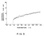
- the tape was dried at about 100°C, pre-treated at 400°C for 1 hour to evaporate off the binder, and heat-treated at 880°C for 10 minutes. After subsequent cooling at a cooling rate of 100°C/hour a superconductive ceramics-laminated tape having a thickness between 5 to 10 ⁇ m and tens of ⁇ m was obtained.
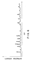
- the crystal orientation was examined by powder X-ray diffractometry. The results are shown in FIG. 4, from which it has been found that the peak of the (00n) plane is so high and intensive that the crystals are strikingly oriented along the c-axis.
- MgO was dry-mixed in a mortar and calcined at 800°C for 10 hours.
- the calcined powders were pulverized in a mortar to a powder size of 280 mesh or less.
- 3 parts by weight of an acrylic resin were added to 10 parts by weight of the calcined product, which step was followed by a 30-minute mixing with a kneader.
- drops of a solvent parapinole and a plasticizer dibutyl phthalate were added to and mixed well with the mixture to obtain an MgO paste.
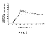
- the MgO paste was formed as a thick film on a Hastelloy tape (a heat-resistant Ni alloy) by screen printing.
- the tape was fired at 900°C for 1 hour to obtain a film thickness of 5 to 10 ⁇ m.
- the obtained composite oxide paste was formed as a thick film on the tape having said intermediate layer by screen printing.
- the film thickness varied from tens of ⁇ m to hundreds of ⁇ m, as measured prior to firing.
- the tape was dried at about 100°C, pre-treated at 400°C for 1 hour to evaporate off the binder, and heat-treated at 860°C for 5 minutes. After subsequent cooling at a cooling rate of 100°C/hour, a superconductive ceramics-laminated tape having a film thickness between 5 to 10 ⁇ m and tens ⁇ m was obtained.
- the crystal orientation was examined by powder X-ray diffractometry. From FIG. 6 showing the results, it has been found that the peak of the (00n) plane is so high and intensive that the crystals are strikingly oriented along the c-axis, that no reaction occurs between the Hastelloy tape and the superconductive ceramics, and that the intermediate layer of MgO promotes orientation and plays a barrier role against diffusion.
- a ceramics laminate was prepared, similarly as described in Example 2, except that a ceramics film was formed on a Hastelloy tape not over any intermediate layer and was examined in terms of its superconductive characteristics.
- the ceramics film provides an electrical insulator, whereby the heat treatment causes it to react with the components of the Hastelloy tape, thus giving rise to a failure of the superconductive phase.
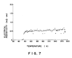
- a ceramics laminate was obtained, similarly as described in Example 2, except that the intermediate layer and substrate were formed of CuO and Ag, respectively, and the film-firing temperature applied was 900°C.
- the laminate was examined in terms of its superconductive characteristics.
- the crystal orientation was examined by powder X-ray diffractometry. From FIG. 8 showing the results, it has been found that the peak of the (00n) plane is so high and intensive that the crystals are strikingly oriented along the c-axis.
- a ceramics laminate was prepared, similarly as described in Example 2, except that the intermediate layer was formed of Ag by plating and the firing temperature applied was 880°C. The laminate was examined in terms of the superconductive characteristics.
- the crystal orientation was examined by powder X-ray diffractometry. From FIG. 10 showing the results, it was found that the peak of the (00n) plane is so high and intensive that the crystals are strikingly oriented along the c-axis.
Landscapes
- Chemical & Material Sciences (AREA)
- Engineering & Computer Science (AREA)
- Ceramic Engineering (AREA)
- Manufacturing & Machinery (AREA)
- Materials Engineering (AREA)
- Structural Engineering (AREA)
- Organic Chemistry (AREA)
- Superconductors And Manufacturing Methods Therefor (AREA)
Applications Claiming Priority (4)
| Application Number | Priority Date | Filing Date | Title |
|---|---|---|---|
| JP80020/88 | 1988-03-31 | ||
| JP63080020A JP2649242B2 (ja) | 1988-03-31 | 1988-03-31 | 超電導セラミックス積層体およびその製造法 |
| JP80021/88 | 1988-03-31 | ||
| JP63080021A JP2532914B2 (ja) | 1988-03-31 | 1988-03-31 | 超電導セラミックス積層体およびその製造法 |
Publications (2)
| Publication Number | Publication Date |
|---|---|
| EP0339801A1 true EP0339801A1 (de) | 1989-11-02 |
| EP0339801B1 EP0339801B1 (de) | 1993-01-27 |
Family
ID=26421047
Family Applications (1)
| Application Number | Title | Priority Date | Filing Date |
|---|---|---|---|
| EP89303174A Expired - Lifetime EP0339801B1 (de) | 1988-03-31 | 1989-03-30 | Dünne supraleitende keramische Schichten und Verfahren zu ihrer Herstellung |
Country Status (3)
| Country | Link |
|---|---|
| US (1) | US5096878A (de) |
| EP (1) | EP0339801B1 (de) |
| DE (1) | DE68904588T2 (de) |
Cited By (8)
| Publication number | Priority date | Publication date | Assignee | Title |
|---|---|---|---|---|
| EP0449317A3 (en) * | 1990-03-29 | 1991-11-27 | Sumitomo Electric Industries, Ltd. | Method of preparing oxide superconducting thin film |
| US5104849A (en) * | 1989-06-06 | 1992-04-14 | The Furukawa Electric Co., Ltd. | Oxide superconductor and method of manufacturing the same |
| EP0488717A1 (de) * | 1990-11-29 | 1992-06-03 | Ngk Insulators, Ltd. | Material aus supraleitendem Oxyd für magnetische Abschirmung und Verfahren zu seiner Herstellung |
| DE4210198A1 (de) * | 1992-03-28 | 1993-09-30 | Dresden Ev Inst Festkoerper | Verfahren zur Herstellung von schmelztexturierten Hochtemperatur-Supraleitern |
| DE4339407A1 (de) * | 1993-11-18 | 1995-05-24 | Dresden Ev Inst Festkoerper | Verfahren zur Herstellung von bandförmigen Hochtemperatur-Supraleitern |
| US5877125A (en) * | 1990-07-16 | 1999-03-02 | Sumitomo Electric Industries, Ltd. | Method of preparing bismuth superconductor |
| WO2000010208A1 (de) * | 1998-08-14 | 2000-02-24 | Abb Research Ltd. | Elektrisch stabilisierter dünnschicht-hochtemperatursupraleiter sowie verfahren zur herstellung eines solchen supraleiters |
| US6812191B2 (en) | 1999-02-17 | 2004-11-02 | Solvay Barium Strontium Gmbh | Superconducting bodies made of zinc-doped copper oxide material |
Families Citing this family (13)
| Publication number | Priority date | Publication date | Assignee | Title |
|---|---|---|---|---|
| FR2667321A1 (fr) * | 1990-09-27 | 1992-04-03 | Etrillard Jackie | Encre serigraphiable supraconductrice et procede de fabrication d'une couche epaisse supraconductrice utilisant cette encre. |
| CA2062709C (en) * | 1991-03-11 | 1997-06-24 | So Tanaka | Superconducting thin film having at least one isolated superconducting region formed of oxide superconductor material and method for manufacturing the same |
| US5304538A (en) * | 1992-03-11 | 1994-04-19 | The United States Of America As Repeated By The Administrator Of The National Aeronautics And Space Administration | Epitaxial heterojunctions of oxide semiconductors and metals on high temperature superconductors |
| US6027826A (en) * | 1994-06-16 | 2000-02-22 | The United States Of America As Represented By The Secretary Of The Air Force | Method for making ceramic-metal composites and the resulting composites |
| US6323549B1 (en) * | 1996-08-29 | 2001-11-27 | L. Pierre deRochemont | Ceramic composite wiring structures for semiconductor devices and method of manufacture |
| JP4174332B2 (ja) * | 2003-01-23 | 2008-10-29 | 財団法人国際超電導産業技術研究センター | 酸化物超電導体の製造方法及び酸化物超電導体とその前駆体支持用基材 |
| US7789326B2 (en) | 2006-12-29 | 2010-09-07 | Water Pik, Inc. | Handheld showerhead with mode control and method of selecting a handheld showerhead mode |
| TWI415528B (zh) * | 2008-04-24 | 2013-11-11 | Kinik Co | 高導熱性電路載板及其製作方法 |
| JP2017533572A (ja) * | 2011-03-30 | 2017-11-09 | アンバチュア インコーポレイテッドAMBATURE Inc. | 非常に低い抵抗材料で形成された、電気的デバイス、機械的デバイス、コンピュータデバイス、および/または、他のデバイス |
| US20180166763A1 (en) | 2016-11-14 | 2018-06-14 | Skyworks Solutions, Inc. | Integrated microstrip and substrate integrated waveguide circulators/isolators formed with co-fired magnetic-dielectric composites |
| JP7115941B2 (ja) | 2017-09-08 | 2022-08-09 | スカイワークス ソリューションズ,インコーポレイテッド | 複合材料の形成方法、及び無線周波数アイソレータ又はサーキュレータの形成方法 |
| US11603333B2 (en) | 2018-04-23 | 2023-03-14 | Skyworks Solutions, Inc. | Modified barium tungstate for co-firing |
| JP7328262B2 (ja) | 2018-06-21 | 2023-08-16 | スカイワークス ソリューションズ,インコーポレイテッド | 複合材料とその形成方法、及び無線周波数アイソレータ又はサーキュレータ |
Citations (1)
| Publication number | Priority date | Publication date | Assignee | Title |
|---|---|---|---|---|
| EP0244993A2 (de) * | 1986-05-09 | 1987-11-11 | Corning Glass Works | Geschichteter Keramikgegenstand |
-
1989
- 1989-03-30 EP EP89303174A patent/EP0339801B1/de not_active Expired - Lifetime
- 1989-03-30 DE DE8989303174T patent/DE68904588T2/de not_active Expired - Fee Related
-
1991
- 1991-01-28 US US07/647,216 patent/US5096878A/en not_active Expired - Fee Related
Patent Citations (1)
| Publication number | Priority date | Publication date | Assignee | Title |
|---|---|---|---|---|
| EP0244993A2 (de) * | 1986-05-09 | 1987-11-11 | Corning Glass Works | Geschichteter Keramikgegenstand |
Non-Patent Citations (3)
| Title |
|---|
| APPLIED PHYSICS LETTERS, vol. 53, no. 17, 24th October 1988, pages 1654-1656, American Institute of Physics; R.D. LORENTZ et al.: "Oriented hig-temperature superconducting Bi-Sr-Ca-Cu-O thin films prepared by ion beam deposition" * |
| JAPANESE JOURNAL OF APPLIED PHYSICS, vol. 27, no. 7, July 1988, pages L1297-L1299; K. HOSHINO et al.: "Preparation of superconducting Bi-Sr-Ca-Cu-O printed thick films on MgO Substrate and Ag metal tape" * |
| PHYSICAL REVIEW, vol. 36, no. 16, 1st December 1987, pages 8903-8906, The American Physical Society; P. CHAUDHARI et al.: "Properties of epitaxial films of YBa2Cu3O7-delta" * |
Cited By (11)
| Publication number | Priority date | Publication date | Assignee | Title |
|---|---|---|---|---|
| US5104849A (en) * | 1989-06-06 | 1992-04-14 | The Furukawa Electric Co., Ltd. | Oxide superconductor and method of manufacturing the same |
| US5232908A (en) * | 1989-06-06 | 1993-08-03 | The Furukawa Electric Co., Ltd. | Method of manufacturing an oxide superconductor/metal laminate |
| EP0449317A3 (en) * | 1990-03-29 | 1991-11-27 | Sumitomo Electric Industries, Ltd. | Method of preparing oxide superconducting thin film |
| US5130296A (en) * | 1990-03-29 | 1992-07-14 | Sumitomo Electric Industries, Ltd. | Method of preparing an oxide superconducting thin film on a substrate with a plurality of grooves |
| US5877125A (en) * | 1990-07-16 | 1999-03-02 | Sumitomo Electric Industries, Ltd. | Method of preparing bismuth superconductor |
| EP0488717A1 (de) * | 1990-11-29 | 1992-06-03 | Ngk Insulators, Ltd. | Material aus supraleitendem Oxyd für magnetische Abschirmung und Verfahren zu seiner Herstellung |
| DE4210198A1 (de) * | 1992-03-28 | 1993-09-30 | Dresden Ev Inst Festkoerper | Verfahren zur Herstellung von schmelztexturierten Hochtemperatur-Supraleitern |
| DE4339407A1 (de) * | 1993-11-18 | 1995-05-24 | Dresden Ev Inst Festkoerper | Verfahren zur Herstellung von bandförmigen Hochtemperatur-Supraleitern |
| WO2000010208A1 (de) * | 1998-08-14 | 2000-02-24 | Abb Research Ltd. | Elektrisch stabilisierter dünnschicht-hochtemperatursupraleiter sowie verfahren zur herstellung eines solchen supraleiters |
| US6552415B1 (en) | 1998-08-14 | 2003-04-22 | Abb Research Ltd | Electrically stabilized thin-film high-temperature superconductor and method for the production thereof |
| US6812191B2 (en) | 1999-02-17 | 2004-11-02 | Solvay Barium Strontium Gmbh | Superconducting bodies made of zinc-doped copper oxide material |
Also Published As
| Publication number | Publication date |
|---|---|
| US5096878A (en) | 1992-03-17 |
| DE68904588T2 (de) | 1993-08-19 |
| EP0339801B1 (de) | 1993-01-27 |
| DE68904588D1 (de) | 1993-03-11 |
Similar Documents
| Publication | Publication Date | Title |
|---|---|---|
| US5096878A (en) | Method for production of bi-containing superconducting ceramics laminates | |
| CA1326976C (en) | Superconducting member | |
| EP0312015B1 (de) | Körper mit supraleitendem Oxid und dessen Herstellungsverfahren | |
| CN1022654C (zh) | 隧道型约瑟夫森器件及其制造方法 | |
| CN1006666B (zh) | 电超导体的组合物 | |
| US4908346A (en) | Crystalline rare earth alkaline earth copper oxide thick film circuit element with superconducting onset transition temperature in excess of 77% | |
| JPH0643268B2 (ja) | 酸化物高温超電導体 | |
| EP0330214B1 (de) | Oxidischer Hochtemperatur-Supraleiter und Verfahren zu seiner Herstellung | |
| JPH10236821A (ja) | 不確定性原理に基づく低異方性高温超伝導体とその製造方法 | |
| JP2649242B2 (ja) | 超電導セラミックス積層体およびその製造法 | |
| US5389603A (en) | Oxide superconductors, and devices and systems comprising such a superconductor | |
| EP0949690A2 (de) | Mg dotierte Hochtemperatur Supraleiter | |
| JP2532914B2 (ja) | 超電導セラミックス積層体およびその製造法 | |
| EP0357500B1 (de) | Verfahren zum Herstellen einer supraleitenden Dünnschicht vom Wismut-Typ | |
| JPH0251806A (ja) | 超電導セラミックス積層体およびその製造法 | |
| JP3856852B2 (ja) | 配向性基板を用いた酸化物超伝導膜の製造方法 | |
| JPH01192758A (ja) | 超伝導セラミックス | |
| JP2703227B2 (ja) | 超電導体装置 | |
| JP3448597B2 (ja) | ビスマス系酸化物超電導複合体及びその製造法 | |
| JP3150718B2 (ja) | 超電導体積層用基板及びそれを用いた超電導積層体 | |
| US5629269A (en) | Process for forming oxide superconducting films with a plurality of metal buffer layers | |
| EP0510201A1 (de) | Verfahren zur herstellung einer dünnen supraleitenden schicht | |
| JPH0251805A (ja) | 超電導セラミックス積層体およびその製造法 | |
| JPH03263392A (ja) | 超電導厚膜回路板及びその製造法 | |
| Poeppel et al. | Processing And Electrical Properties Of High-Tc Superconductors |
Legal Events
| Date | Code | Title | Description |
|---|---|---|---|
| PUAI | Public reference made under article 153(3) epc to a published international application that has entered the european phase |
Free format text: ORIGINAL CODE: 0009012 |
|
| AK | Designated contracting states |
Kind code of ref document: A1 Designated state(s): BE DE FR GB NL SE |
|
| 17P | Request for examination filed |
Effective date: 19891108 |
|
| RAP1 | Party data changed (applicant data changed or rights of an application transferred) |
Owner name: NATIONAL RESEARCH INSTITUTE FOR METALS, SCIENCE A Owner name: MITSUI KINZOKU KOGYO KABUSHIKI KAISHA |
|
| 17Q | First examination report despatched |
Effective date: 19910808 |
|
| GRAA | (expected) grant |
Free format text: ORIGINAL CODE: 0009210 |
|
| AK | Designated contracting states |
Kind code of ref document: B1 Designated state(s): BE DE FR GB NL SE |
|
| REF | Corresponds to: |
Ref document number: 68904588 Country of ref document: DE Date of ref document: 19930311 |
|
| ET | Fr: translation filed | ||
| PLBI | Opposition filed |
Free format text: ORIGINAL CODE: 0009260 |
|
| 26 | Opposition filed |
Opponent name: SIEMENS AG ZFE GR PA Z Effective date: 19931013 |
|
| NLR1 | Nl: opposition has been filed with the epo |
Opponent name: SIEMENS AG. |
|
| EAL | Se: european patent in force in sweden |
Ref document number: 89303174.0 |
|
| PLBN | Opposition rejected |
Free format text: ORIGINAL CODE: 0009273 |
|
| STAA | Information on the status of an ep patent application or granted ep patent |
Free format text: STATUS: OPPOSITION REJECTED |
|
| 27O | Opposition rejected |
Effective date: 19950601 |
|
| NLR2 | Nl: decision of opposition | ||
| PGFP | Annual fee paid to national office [announced via postgrant information from national office to epo] |
Ref country code: BE Payment date: 19960219 Year of fee payment: 8 |
|
| PGFP | Annual fee paid to national office [announced via postgrant information from national office to epo] |
Ref country code: SE Payment date: 19960318 Year of fee payment: 8 |
|
| PGFP | Annual fee paid to national office [announced via postgrant information from national office to epo] |
Ref country code: FR Payment date: 19960328 Year of fee payment: 8 |
|
| PGFP | Annual fee paid to national office [announced via postgrant information from national office to epo] |
Ref country code: NL Payment date: 19960331 Year of fee payment: 8 |
|
| PGFP | Annual fee paid to national office [announced via postgrant information from national office to epo] |
Ref country code: GB Payment date: 19970321 Year of fee payment: 9 |
|
| PG25 | Lapsed in a contracting state [announced via postgrant information from national office to epo] |
Ref country code: SE Effective date: 19970331 Ref country code: BE Effective date: 19970331 |
|
| PGFP | Annual fee paid to national office [announced via postgrant information from national office to epo] |
Ref country code: DE Payment date: 19970524 Year of fee payment: 9 |
|
| BERE | Be: lapsed |
Owner name: NATIONAL RESEARCH INSTITUTE FOR METALS SCIENCE AN Effective date: 19970331 Owner name: MITSUI KINZOKU KOGYO K.K. Effective date: 19970331 |
|
| PG25 | Lapsed in a contracting state [announced via postgrant information from national office to epo] |
Ref country code: NL Effective date: 19971001 |
|
| PG25 | Lapsed in a contracting state [announced via postgrant information from national office to epo] |
Ref country code: FR Free format text: LAPSE BECAUSE OF NON-PAYMENT OF DUE FEES Effective date: 19971128 |
|
| NLV4 | Nl: lapsed or anulled due to non-payment of the annual fee |
Effective date: 19971001 |
|
| EUG | Se: european patent has lapsed |
Ref document number: 89303174.0 |
|
| REG | Reference to a national code |
Ref country code: FR Ref legal event code: ST |
|
| PG25 | Lapsed in a contracting state [announced via postgrant information from national office to epo] |
Ref country code: GB Free format text: LAPSE BECAUSE OF NON-PAYMENT OF DUE FEES Effective date: 19980330 |
|
| GBPC | Gb: european patent ceased through non-payment of renewal fee |
Effective date: 19980330 |
|
| PG25 | Lapsed in a contracting state [announced via postgrant information from national office to epo] |
Ref country code: DE Free format text: LAPSE BECAUSE OF NON-PAYMENT OF DUE FEES Effective date: 19981201 |