EP0337471B1 - Schaltung mit seriellem Ein- und Ausgang zur Ausgabe von Bits aus Zweirichtungsschieberegistern, entweder in Vorwärts- oder Umkehrreihenfolge - Google Patents
Schaltung mit seriellem Ein- und Ausgang zur Ausgabe von Bits aus Zweirichtungsschieberegistern, entweder in Vorwärts- oder Umkehrreihenfolge Download PDFInfo
- Publication number
- EP0337471B1 EP0337471B1 EP89106648A EP89106648A EP0337471B1 EP 0337471 B1 EP0337471 B1 EP 0337471B1 EP 89106648 A EP89106648 A EP 89106648A EP 89106648 A EP89106648 A EP 89106648A EP 0337471 B1 EP0337471 B1 EP 0337471B1
- Authority
- EP
- European Patent Office
- Prior art keywords
- bit
- bits
- input
- output
- serial
- Prior art date
- Legal status (The legal status is an assumption and is not a legal conclusion. Google has not performed a legal analysis and makes no representation as to the accuracy of the status listed.)
- Expired - Lifetime
Links
Images

Classifications
-
- G—PHYSICS
- G06—COMPUTING OR CALCULATING; COUNTING
- G06F—ELECTRIC DIGITAL DATA PROCESSING
- G06F7/00—Methods or arrangements for processing data by operating upon the order or content of the data handled
- G06F7/76—Arrangements for rearranging, permuting or selecting data according to predetermined rules, independently of the content of the data
- G06F7/78—Arrangements for rearranging, permuting or selecting data according to predetermined rules, independently of the content of the data for changing the order of data flow, e.g. matrix transposition or LIFO buffers; Overflow or underflow handling therefor
- G06F7/785—Arrangements for rearranging, permuting or selecting data according to predetermined rules, independently of the content of the data for changing the order of data flow, e.g. matrix transposition or LIFO buffers; Overflow or underflow handling therefor having a sequence of storage locations each being individually accessible for both enqueue and dequeue operations, e.g. using a RAM
Definitions
- This invention relates to a serial input-output circuit which has a circuit input terminal supplied with an input serial bit sequence and is for use as an interface between the input terminal and a processing circuit for processing an output serial bit sequence supplied from the serial input-output circuit selectively forwardly and backwardly of the input serial bit sequence.
- the prior art serial input-output circuit comprises an input shift register supplied with the input serial bit sequence for producing a sequence of output bit groups, each consisting of a first predetermined number of parallel bits.
- a memory device is used to memorize the parallel bits of the output bit groups as parallel bits of memorized bit groups.
- a producing arrangement includes a series connection of first and second bidirectional or right-left shift registers and is connected to the memory device to produce a predetermined part of the memorized bit groups as the output serial bit sequence forwardly and backwardly as regards time relative to the input serial bit sequence.
- Each of the first and the second (bidirectional) shift registers may have a memory capacity for one memorized bit group.
- a first selected one of the memorized bit groups is read bit parallel from the memory device into a parallel-to-series converter.
- the parallel bits of the first selected bit group are stored in bit series or sequence in the first shift register. It is possible while shifting the parallel bits in bit series forward from the first shift register to the second one to successively store the parallel bits of a second selected one of the memorized bit groups in bit series from the converter in the first shift register. In this manner, the parallel bits of two memorized bit groups are held as total held bits at a time in the first and the second shift registers.
- the second selected bit group next follows the first selected bit group in the input serial bit sequence.
- the total held bits are therefore arranged in the first and the second shift registers from an earliest bit to a latest bit. More particularly, the earliest bit is one of the parallel bits of the first selected bit group that is earliest stored in the first shift register from the converter. The latest bit is one of the parallel bits of the second selected bit group that is latest stored in the first shift register from the converter. While subjected to a forward shift from the first shift register to the second one, the held bits are delivered from the second shift register to the other of the two input terminals of the intermediate selector and from the intermediate selector to the first shift register. In this manner, the total held bits are circulated through the first and the second shift registers and the intermediate selector with the latest bit followed by the earliest bit.
- the intermediate selector On subjecting the total held bits to a backward shift from the second shift register to the first one, the intermediate selector is not used.
- the total held bits are merely repeatedly circulated through the second and the first shift registers with the earliest bit followed by the latest bit.
- this serial input-output circuit has a limited value when the first and second bidirectional shift registers shift backwardly. It is possible to vary the limited value either by giving a large memory capacity to the second bidirectional shift register or by additionally using another bidirectional shift register. This is, however, undesirable in implementing ; the serial input-output circuit by an integrated circuit.
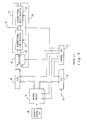
- a conventional serial input-output circuit will be described at first in order to facilitate an understanding of the present invention.
- the conventional serial input-output circuit is designed as a prior art serial input-output circuit with reference to the Forney, Jr., et al article cited heretobefore.
- the serial input-output circuit has circuit input and output terminals 11 and 12.
- the circuit input terminal 11 is supplied with an input serial bit sequence consisting of input serial bits.
- the serial input-output circuit is for delivering an output serial bit sequence of output serial bits through the circuit output terminal 12 to a processing circuit with the output serial bit sequence moved selectively forwardly and backwardly of the input serial bit sequence, namely, with the output serial bits arranged selectively forwardly and backwardly along the input serial bits. If necessary, it is possible to understand that the processing circuit is depicted at 12.
- An input shift register 13 is supplied with the input serial bit sequence in bit series or sequence through the circuit input terminal 11 and bit parallel produces a sequence of output bit groups, each consisting of a first predetermined number of parallel bits.
- the input shift register 13 therefore serves as a series-to-parallel (S/P) converter and is so labelled in Fig. 1.
- a memory device 15 has a plurality of memory sectors, each for memorizing the parallel bits of one of the output bit groups as parallel bits of a memorized bit group and for bit parallel producing the parallel bits of the memorized bit group.
- An address generator 16 is used to indicate the memory sectors one at a time.
- a control circuit 17 is for making, among others, the input shift register 13 produce each output bit group for write (W) in the memory device 15, making the address generator 16 specify one of the memory sectors.
- the control circuit 17 controls the address generator 16 through a connection which is not depicted merely for simplicity of the illustration.
- An intermediate shift register 18 is for memorizing each memorized bit group and serves as a parallel-to-series (P/S) converter.
- An intermediate selector 19 has first and second input terminals and a single output terminal. The first and the second input terminals are indicated by 1 (one) and 0 (zero).
- a series connection of first and second bidirectional or right-left shift registers 21 and 22 is connected to the single output terminal of the intermediate selector 19. More particularly, the first (bidirectional) shift register 21 has a first forward or right and a first backward or left input terminal and a first forward and a first backward output terminal.
- the second shift register 22 has a second forward and a second backward input terminal and a second forward and a second backward output terminal. By a first connection, the first forward output terminal is connected to the second forward input terminal. By a second connection, the secondbackwardoutput terminal is connected to the first backward input terminal.
- the circuit output terminal 12 is connected to a point of connection between the second connection and the second backward output terminal.
- An input connection 23 is used to connect the single output terminal of the intermediate selector 19 to the first forward input terminal.
- each of the first and the second shift registers 21 and 22 has a memory capacity for one memorized bit group.
- the parallel bits of two memorized bit groups are held in the shift registers 21 and 22 at a time as total held bits.
- the control circuit 17 controls the shift registers 21 and 22 so that the held bits may be subjected selectively to a forward shift from the first shift register 21 to the second shift register 22 and to a backward shift from the second shift register 22 to the first shift register 21.
- a first selected one of the memorized bit groups is read (R) bit parallel from the memory device 15 into the intermediate shift register 18.
- the control circuit 17 is furthermore used to select the first input terminal of the intermediate selector 19, to carry out the forward shift, and to make the intermediate shift register 18 produce the parallel bits of the first selected bit group in bit series so that the parallel bits of the first selected bit group are stored in the first shift register 21 as partial held bits.
- the intermediate shift register 18 can be loaded bit parallel with the parallel bits of a second selected one of the memorized bit groups. It is possible while carrying out the forward shift to store the second selected bit group in bit series in the first shift register 21 through the intermediate selector 19 and the input connection 23. In this manner, the above-mentioned total held bits are held in the shift registers 21 and 22.
- the second selected bit group next follows the first selected bit group when attention is directed to the input serial bit sequence.
- the total held bits are therefore arranged in the first and the second shift registers 21 and 22 from an earliest bit to a latest bit. More specifically, the earliest bit is one of the parallel bits of the first selected bit group that is earliest stored in the first shift register 21 from the intermediate shift register 18 through the intermediate selector 19 and the input connection 23.
- the latest bit is one of the parallel bits of the second selected bit group that is latest stored in the first shift register 21,
- the total held bits are circulated through the first and the second shift registers 21 and 22, the forward connection 24, the intermediate selector 19, and the input connection 23.
- the intermediate selector 19 On subjecting the total held bits merely to the backward shift, the intermediate selector 19 is not used.
- the held bits are repeatedly circulated through the second and the first shift registers 22 and 21 and through the backward connection 25.
- this serial input-output has a limited value when the first and second bridirectional shift registers 21 and 22 shift backwardly. It is possible to vary the limited either by giving a large memory capacity to the second bidirectional shift register 22 or by additionally using another bidirectional shift register (not shown). This is, however, undesirable in implementing the serial input-output circuit by an integrated circuit.
- a combination of the intermediate shift register 18, the intermediate selector 19, and the first and the second bidirectional shift registers 21 and 22 serves as an output arrangement in cooperation with the address generator 16, the control circuit 17, and others.
- the output arrangement produces a predetermined part of the memorized bit groups, such as the second or the third predetermined number of bits, as the output serial bit sequence selectively forwardly and backwardly of the input serial bit sequence.
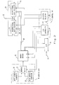
- Figs. 2 and 3 the description will proceed to a serial input-output circuit according to a preferred embodiment of the instant invention. Similar parts are designated by like reference numerals and are likewise operable. It is to be noted in connection with Fig. 2 that the address generator 16 and the control circuit 17 are depicted more in detail, that the intermediate shift register 18 and selector 19 are excluded together with the input connection 23, and that the control circuit 17 is operable accordingly simpler than that described in connection with Fig. 1.
- the first and the second connections may alternatively be referred to collectively as a bidirectional connection.
- the forward and the backward connections 24 and 25 may collectively be called a ring connection. It should, however, be noted that the forward and the backward connections 24 and 25 are for shifting the total held bits forwardly or rightwardly of the figure and backwardly or leftwards, respectively.
- the address generator 16 comprises a write address generator 31 for generating a write address signal indicative of the memory sectors of the memory device 15 for write (W).
- a read address generator 32 generates a read address signal indicative of one of the memory sectors for read (R).
- An address selector 33 is for supplying the memory device 15 selectively with the write and the read address signals.
- the control circuit 17 comprises an input-output controller 34 for controlling the input shift register 13, write and read of the memory device 15, and the address selector 33.
- a register selector 35 is connected to the first and the second bidirectional shift registers 21 and 22 to simultaneously make the shift registers 21 and 22 carry out one of the forward and the backward shifts and to select one of the first and the second (bidirectional) shift registers 21 and 22 as a selected shift register for bit parallel load of the parallel bits of one of the memorized bit groups that is memorized in the memory device 15 at the memory sector accessed by the read address signal and is produced from the memory device 15 as a selected bit group.
- the input-output controller 34 controls the register selector 35 for selection of the selected shift register.
- the input-output controller 34 makes the register selector 35 carry out bit parallel load of the selected bit group on the selected shift register.
- the input-output controller 34 may be manually controlled for the simultaneous forward and backward shifts and for the bit parallel load on the selected shift register. Like an input-output controller which is included in the control circuit 17 described in conjunction with Fig. 1, the input-output controller 34 is so controlled in practice by the processing circuit.
- first and second bit parallel connections 36 and 37 are connected to the first and the second shift registers 21 and 22 and to a common bit parallel connection 38, which is connected directly to the memory divice 15. It is therefore possible to understand that the first and the second bit parallel connections 36 and 37 are connected directly to the memory device 15. Through one of the first and the second bit parallel connections 36 and 37 that is connected to the selected shift register, the memory device 15 bit parallel supplies the parallel bits of the selected bit group to the selected shift register.
- the register selector 35 serves in cooperation with the input-output controller 34 as a register selecting arrangement for selecting the selected shift register.
- a combination of the read address generator 32 and the address selector 33 serves as a group selecting arrangement for selecting the selected bit group.
- the above-mentioned other L of the two control leads serves as a supplying arrangement for supplying the selected bit group to the selected shift register.
- a combination of the first and the second bit parallel connections 36 and 37 serves in cooperation with the register selecting arrangement, the group selecting arrangement, and the supplying arrangement as a storing arrangement for bit parallel storing the parallel bits of the selected bit group as the afore-mentioned partial bits in the selected shift register.
- the ring connection namely, a combination of the forward and the backward connections 24 and 25, serves in cooperation with the bidirectional connection and with a shift or clock pulse generator as a shifting arrangement for selectively forwadly and backwardly shifting through the first and the second shift registers 21 and 22 the total held bits which are held in the first and the second shift registers 21 and 22 and consist of two groups of partial held bits.
- the shift pulse generator is not depicted merely for simplicity of the illustration. If necessary, the forward and the backward connections 24 and 25 should be understood to represent the shift pulse generator.
- the circuit output terminal 12 may alternatively be called a producing arrangement.
- a ccmbination of the first and the second shift registers 21 and 22, the storing arrangement, the shifting arrangement, and the producing arrangement serves as the output arrangement mentioned in connection with the conventional series input-output circuit.
- the output arrangement is astonishingly simple in structure and is unexpectedly excellently operable in the input-output circuit being illustrated in the manner which will become clear later in the following.
- each of the input shift register 13 and the first and the second shift registers 21 and 22 has a memory capacity of a first predetermined number K of bits.
- each of the shift registers 13, 21, and 22 has zeroth through (K-1)-th stages controlled by the shift pulse generator mentioned before.
- the zeroth stage serves as the first forward input and the first backward output terminals.
- the (K-1)-th stage serves as the first forward output and the first backward input terminals.
- the zeroth stage serves as the second forward input and the second backward output terminals.
- the (K-1)-th stage serves as the second forward output and the second backward input terminals.
- the first predetermined number K may typically be equal to eight.
- the memory device 15 may have 1,024 memory sectors, each for K parallel bits. Depending on the circumstances, the memory sectors will be numbered from a zeroth memory sector up to a 1,023-rd one.
- the input-output controller 34 can monitor the input and the first and the second shift registers 13, 21, and 22 and can detect a request for production of an output serial bit sequence.
- the circuit input terminal 11 be supplied with an input serial bit sequence consisting of zeroth, first, and other binary bits a(0), a(1), and so forth.
- the input-output controller 34 makes the write address generator 31 produce the write address signal with indication of the zeroth memory sector of the memory device 15, controls the address selector 33 so as to select the write address signal, and energizes the memory device 15 for bit parallel storage of the zeroth through the (K-1)-th binary bits in the zeroth memory sector as the parallel bits of a zeroth memorized bit group.
- the output bit groups of the input shift register 13 are successively stored in the first and other memory sectors of the memory device 15 as first, second, and other memorized bit groups.
- the input-output controller 34 makes the read address generator 32 produce the read address signal with indication of the zeroth memory sector of the memory device 15, controls the address selector 33 so as to select this read address signal, and energizes the memory device 15 for bit parallel delivery of the zeroth through the (K-1)-th bits of the zeroth memorized bit group as the parallel bits of the selected bit group to the common bit parallel connection 38.
- the input-output controller 34 furthermore makes the register selector 35 select the first shift register 21 as the selected shift register and bit parallel loads the selected shift register with the zeroth through the (K-1)-th bits as the partial held bits through the first bit parallel connection 36.
- the read address signal is made to indicate the first memory sector.
- the address selector 33 is kept to select the read address signal.
- the register selector 35 is kept to select the first shift register 21 as the selected shift register.
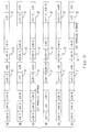
- Fig. 3 the zeroth through the (K-1)-th stages of the first and the second shift registers 21 and 22 are depicted from left to right.
- an initial state depicted along a first or top line labelled (A) the zeroth through the (2K-1)-th bits are held as the total held bits in the second and the first shift registers 22 and 21.
- the zeroth and the (2K-1)-th bits are the earliest and the latest bits described before despite simultaneous storage of the zeroth through the (K-1)-th bits and of the K-th through the (2K-1)-th bits.
- the input-output controller 34 detects a first request for production of a predetermined part of the memorized bit groups through the circuit output terminal 12 as the output serial bit sequence and that the output serial bit sequence should consist of a second predetermined number, such as (K + 2), of output binary bits which start at a predetermined one of the total held bits, such as the K-th bit a(K), and should be produced forwardly as regards time relative to the input serial bit sequence.
- the total held bits are forwardly shifted to an intermediate state illustrated along a second line labelled (B).
- each held bit is delivered to the circuit output terminal 12 as one of the output binary bits.
- the output serial bit sequence should include the 2K-th and the (2K+1)-th bits which follow the latest bit a(2K - 1) and are not held in the first and the second shift registers 21 and 22. This fact is senses by the input-output controller 24 in the known manner.
- the input-output controller 34 therefore makes the read address generator 32 generate the read address signal with indication of the second memory sector of the memory device 15.
- the 2K-th through the (3K-1)-th bits of the second memorized bit group are bit parallel stored from the memory device 15 in the first shift register 21 as fresh partial held bits through the first bit parallel connection 36. It will be understood that the parallel bits of the second memorized bit group are substituted in the total held bits for the parallel bits of the zeroth memorized bit group.
- the total held bits become as illustrated in Fig. 3 along a third line labelled (C).
- the forward shift is continued two more stages or bits to produce the 2K-th and the (2K+1)-th bits as a trailing part of the output serial bit sequence.
- the input-output controller 34 suspends the forward shift.
- the total held bits become as depicted in Fig. 3 along a fourth line labelled (D). It will be seen that the total held bits are forward shifted (2K + 2) bits from the initial state illustrated in the first line (A) to a suspended state depicted in the fourth line (D) with the second memorized bit group substituted in the suspended state for the zeroth memorized bit group.
- the K-th and the (3K-1)-th bits afresh become the earliest and the latest bits.
- the input-output controller 34 detects a second request for a (2K+2)-bit backward shift from the suspended state as regards time relative to the input serial bit sequence.
- (2K + 2) output binary bits are produced as the output serial bit sequence starting at one of the total held bits that is held in the suspended state in the zeroth stage of the second shift register 22.
- the backward shift is back to the earliest bit a(K). Sensing this fact, the input-output controller 34 carries through the backward shift without substituting a certain one of the memorized bit groups for either of the two selected bit groups which are held in the first and the second shift registers 21 and 22 as the total held bits.
- the backward shift should be carried out in connection with a third predetermined number of output binary bits including at least one of the parallel bits of the memorized bit groups, such as the (K-1)-th bit and at least one earlier or more backward bit, that is not included in the total held bits in the suspended state depicted in Fig. 3 along the fourth line (D)
- this fact is senses by the input-output controller 34 in the known manner together with a progress of the backward shift to another intermediate state illustrated in Fig. 3 along a fifth line labelled (E).
- the input-output controller 34 thereupon makes the read address signal indicate one of the memorized bit groups that precedes the partial held bits including the earliest bit.
- the above-mentioned one of the memorized bit groups is the zeroth memorized bit group.
- the input-output controller 34 makes the read address signal indicate the zeroth memory sector of the memory device 15, controls the address selector 33 so as to select the last-mentioned read address signal, controls the register selector 35 so as to select the second shift register 22 as the selected shift register, and energizes the memory device 15 for bit parallel delivery of the parallel bits of the zeroth memorized bit group to the common bit parallel connection 38.
- the input-output controller 34 furthermore makes the register selector 35 load the second shift register 22 bit parallel with the parallel bits of the zeroth memorized bit group through the second bit parallel connection 37.
- the earliest and the latest bits are two of the parallel bits of two succcessively selected bit groups and are supplied earliest and latest to the selected shift register as regards the forward shift of the total held bits through the first and the second shift registers 21 and 22. More particularly, the earliest and the latest bits are supplied earliest and latest if the parallel bits of the two successively selected bit groups were bit series supplied to the first shift register 21 rather than bit parallel.
- the register selecting arrangement selects a particular one of the first and the second shift registers 21 and 22 as the selected shift register that holds the earliest and the latest bits if at least one, such as a(2K) or a(K - 1), should be produced in the output serial bit sequence following the latest and the earliest bits while the output serial bit sequence is produced forwardly and backwardly of the input serial bit sequence, respectively.
- the group selecting arrangement selects as a single selected bit group one of the memorized bit groups that follows and precedes the two successively selected bit groups.
- the supplying arrangement supplies the parallel bits of the single selected bit group bit parallel to the particular one of the first and the second shift registers 21 and 22.
- a plurality of binary bits are depicted in a simple tree structure. That is, zeroth through fifteenth paths start from an origin O (oh) and end at zeroth through fifteenth end points P(0) to P(15) passing through intermediate nodes, The origin and the end points are also nodes. Only one binary bit, namely, a binary zero or one bit, is assigned to a path part between two adjacent nodes. When viewed from the origin towards the end points, a path part regularly branches into two path parts.
- the processing circuit may be used to locate an optimum path from the origin to an optimum end point.
- the zeroth and other input serial bits may represent the binary bits along the zeroth path, the binary bit of the path part ending at the first end point P(1), and so on.
- the serial input-output circuit help the processing one that can produce various output serial bit sequences with the path parts readily forwardly traced from the origin to the end points returning backwardly either to the origin or to a selected one of the intermediate nodes.
- a plurality of binary bits may be assigned to each path part.
- the number of intermediate nodes may be different depending on the paths between the origin and the end points. If the output serial bit sequence should start at a prescribed one of the parallel bits of the memorized bit groups that is not included in the total held bits at a time, the held bits should be renewed under the control of the input-output controller 34 so that the prescribed bit should be stored in one of the first and the second shift registers 21 and 22.
- the circuit outpout 12 may differently be connected to a selected one of the first and the second bidirectional shift registers 21 and 22.
- the serial input-output circuit may be used as an interface between the circuit input terminal 11 and the circuit output terminal 12 which is connected to a bit serial error detecting and correcting circuit.
Landscapes
- Physics & Mathematics (AREA)
- Engineering & Computer Science (AREA)
- Theoretical Computer Science (AREA)
- Mathematical Physics (AREA)
- General Engineering & Computer Science (AREA)
- General Physics & Mathematics (AREA)
- Shift Register Type Memory (AREA)
- Communication Control (AREA)
- Executing Machine-Instructions (AREA)
- Compression, Expansion, Code Conversion, And Decoders (AREA)
Claims (4)
- Serielle Eingangs/Ausgangsschaltung, die folgendes aufweist:ein Eingangs-Schieberegister (13), dem zum Erzeugen einer Folge von Ausgangsbitgruppen, die jeweils aus einer ersten vorbestimmten Anzahl paralleler Bits bestehen, eine serielle Eingangsbitfolge zugeführt wird,eine Speichervorrichtung (15) zum Speichern der Ausgangsbitgruppen als gespeicherte Bitgruppen,jeweils für eine der gespeicherten Bitgruppen ein erstes und ein zweites bidirektionales Schieberegister (21, 22),eine Steuereinrichtung (34, 35, 36, 37), die mit der Speichervorrichtung (15) und dem ersten und dem zweiten bidirektionalen Schieberegister (21, 22) verbunden ist,eine Schiebeeinrichtung (24, 25) zum bidirektionalen Verschieben aller gehaltenen Bits, die in dem ersten und dem zweiten bidirektionalen Schieberegister (21, 22) in einer Ringverbindung gehalten sind, undeine Erzeugungseinrichtung (12), die mit einem von dem ersten und dem zweiten bidirektionalen Schieberegister (21, 22) verbunden ist, zum Erzeugeneines vorbestimmten Teils der gespeicherten Bitgruppen selektiv nach rechts oder links eines vorbestimmten aller gehaltenen Bits, die in dem ersten und dem zweiten bidirektionalen Schieberegister (21, 22) enthalten sind, als serielle Ausgangsbitfolge,dadurch gekennzeichnet, daß
die Steuereinrichtung (17) sowohl das zirkulare bidirektionale Verschieben der Gesamtheit der gehaltenen Bits steuert, die im ersten und im zweiten bidirektionalen Schieberegister (21, 22) gehalten sind, als auch das bitparallele Laden von der Speichervorrichtung einer ausgewählten der gespeicherten Bitgruppen als Teil der gehaltenen Bits in ein ausgewähltes von dem ersten und dem zweiten bidirektionalen Schieberegister (21, 22) bezüglich der Bitposition des vorbestimmten der gesamten gehaltenen Bits und bezüglich einer Funktion der Anzahl der Bits, die im vorbestimmten Teil der gespeicherten Bitgruppen enthalten sind. - Serielle Eingangs/Ausgangsschaltung nach Anspruch 1, wobei das erste bidirektionale Schieberegister (21) einen ersten Vorwärts- und einen ersten Rückwärtseingangsanschluß und einen ersten Vorwärts- und einen ersten Rückwärtsausgangsanschluß aufweist, wobei das zweite bidirektionale Schieberegister (22) einen zweiten Vorwärts- und einen zweiten Rückwärtseingangsanschluß und einen zweiten Vorwärts- und einen zweiten Rückwärtsausgangsanschluß aufweist, wobei die Schiebeeinrichtung (24, 25) eine bidirektionale Verbindung zwischen dem ersten Vorwärtsausgangsanschluß und dem zweiten Vorwärtseingangsanschluß und zwischen dem zweiten Rückwärtsausgangsanschluß und dem ersten Rückwärtseingangsanschluß enthält, wobei:die Schiebeeinrichtung (24, 25) zum selektiven Schieben der gesamten gehaltenen Bits in Rückwärtsrichtung und in Vorwärtsrichtung eine Ringverbindung aufweist, die den ersten Rückwärtsausgangsanschluß mit dem zweiten Rückwärtseingangsanschluß verbindet und den zweiten Vorwärtsausgangsanschluß direkt mit dem ersten Vorwärtseingangsanschluß verbindet; unddie Erzeugungseinrichtung (12) mit dem zweiten Rückwärtsausgangsanschluß verbunden ist.
- Serielle Eingangs/Ausgangsschaltung nach Anspruch 1, wobei die Speichereinrichtung folgendes aufweist:eine erste und eine zweite bitparallele Verbindung (36, 37), die jeweils mit dem ersten und dem zweiten bidirektionalen Schieberegister (21, 22) und direkt mit der Speichervorrichtung (15) verbunden sind;eine Registerauswahleinrichtung (34, 35) zum Auswählen eines von dem ersten und dem zweiten bidirektionalen Schieberegister (21, 22) als ausgewähltes Schieberegister;eine Gruppenauswahleinrichtung (33), die mit der Speichervorrichtung (15, 16) zum Auswählen einer der gespeicherten Bitgruppen als ausgewählte Bitgruppe verbunden ist; undeine Zuführeinrichtung, die mit der ersten und der zweiten bitparallelen Verbindung (36, 37) und mit der Gruppenauswahleinrichtung (33) verbunden ist, zum Zuführen der ausgewählten Bitgruppe zum ausgewählten Schieberegister.
- Serielle Eingangs/Ausgangsschaltung nach Anspruch 3, wobei die gesamten gehaltenen Bits ein erstes und ein letztes Bit enthalten, die zwei der parallelen Bits zweier aufeinanderfolgend ausgewählter Bitgruppen sind und in der seriellen Eingangsbitfolge als erstes und als letztes angeordnet sind, wobei:die Registerauswahleinrichtung (34, 35) ein bestimmtes von dem ersten und dem zweiten bidirektionalen Schieberegister (21, 22) als das ausgewählte Schieberegister auswählt, das das erste und das letzte Bit hält, wenn wenigstens eines der parallelen Bits der gespeicherten Bitgruppen in der seriellen Ausgangsbitfolge erzeugt werden soll, die dem letzten und dem ersten Bit folgt, während die serielle Ausgangsbitfolge jeweils in Vorwärtsrichtung und in Rückwärtsrichtung der seriellen Eingangsfolge erzeugt wird;die Gruppenauswahleinrichtung (33) als einzige ausgewählte Bitgruppe eine der gespeicherten Bitgruppen auswählt, die den zwei aufeinanderfolgend ausgewählten Bitgruppen folgt und vorangeht; unddie Zuführeinrichtung die einzige ausgewählte Bitgruppe dem bestimmten von dem ersten und dem zweiten bidirektionalen Schieberegister (21, 22) zuführt.
Applications Claiming Priority (2)
| Application Number | Priority Date | Filing Date | Title |
|---|---|---|---|
| JP92831/88 | 1988-04-14 | ||
| JP63092831A JP2944084B2 (ja) | 1988-04-14 | 1988-04-14 | シリアル入出力回路 |
Publications (3)
| Publication Number | Publication Date |
|---|---|
| EP0337471A2 EP0337471A2 (de) | 1989-10-18 |
| EP0337471A3 EP0337471A3 (de) | 1991-07-24 |
| EP0337471B1 true EP0337471B1 (de) | 1996-12-18 |
Family
ID=14065379
Family Applications (1)
| Application Number | Title | Priority Date | Filing Date |
|---|---|---|---|
| EP89106648A Expired - Lifetime EP0337471B1 (de) | 1988-04-14 | 1989-04-13 | Schaltung mit seriellem Ein- und Ausgang zur Ausgabe von Bits aus Zweirichtungsschieberegistern, entweder in Vorwärts- oder Umkehrreihenfolge |
Country Status (5)
| Country | Link |
|---|---|
| US (1) | US4959813A (de) |
| EP (1) | EP0337471B1 (de) |
| JP (1) | JP2944084B2 (de) |
| AU (1) | AU618707B2 (de) |
| DE (1) | DE68927559T2 (de) |
Families Citing this family (6)
| Publication number | Priority date | Publication date | Assignee | Title |
|---|---|---|---|---|
| JPH02217918A (ja) * | 1989-02-17 | 1990-08-30 | Nec Eng Ltd | メモリインタフェース回路 |
| US5206834A (en) * | 1989-10-14 | 1993-04-27 | Mitsubishi Denki Kabushiki Kaisha | Semiconductor memory device performing last in-first out operation and the method for controlling the same |
| JP3118266B2 (ja) * | 1990-03-06 | 2000-12-18 | ゼロックス コーポレイション | 同期セグメントバスとバス通信方法 |
| US5327571A (en) * | 1990-04-03 | 1994-07-05 | Advanced Micro Devices, Inc. | Processor having decoder for decoding unmodified instruction set for addressing register to read or write in parallel or serially shift in from left or right |
| JP3636497B2 (ja) * | 1995-02-27 | 2005-04-06 | 株式会社ルネサステクノロジ | 半導体集積回路装置 |
| JPH103436A (ja) * | 1996-06-17 | 1998-01-06 | Mitsubishi Electric Corp | 自動転送機能付シリアル入出力回路 |
Family Cites Families (6)
| Publication number | Priority date | Publication date | Assignee | Title |
|---|---|---|---|---|
| JPS56128751U (de) * | 1980-02-29 | 1981-09-30 | ||
| JPS59177674A (ja) * | 1983-03-29 | 1984-10-08 | Yokogawa Hokushin Electric Corp | 画像処理装置 |
| JPS607678A (ja) * | 1983-06-25 | 1985-01-16 | Fujitsu Ltd | メモリ構成方式 |
| JPS61236094A (ja) * | 1985-04-10 | 1986-10-21 | Fujitsu Ltd | 直列デ−タ入力メモリ |
| US4864544A (en) * | 1986-03-12 | 1989-09-05 | Advanced Micro Devices, Inc. | A Ram cell having means for controlling a bidirectional shift |
| US4813015A (en) * | 1986-03-12 | 1989-03-14 | Advanced Micro Devices, Inc. | Fracturable x-y storage array using a ram cell with bidirectional shift |
-
1988
- 1988-04-14 JP JP63092831A patent/JP2944084B2/ja not_active Expired - Fee Related
-
1989
- 1989-04-13 EP EP89106648A patent/EP0337471B1/de not_active Expired - Lifetime
- 1989-04-13 DE DE68927559T patent/DE68927559T2/de not_active Expired - Fee Related
- 1989-04-14 AU AU33031/89A patent/AU618707B2/en not_active Ceased
- 1989-04-14 US US07/338,070 patent/US4959813A/en not_active Expired - Lifetime
Also Published As
| Publication number | Publication date |
|---|---|
| EP0337471A3 (de) | 1991-07-24 |
| AU618707B2 (en) | 1992-01-02 |
| AU3303189A (en) | 1989-10-19 |
| JP2944084B2 (ja) | 1999-08-30 |
| JPH02161519A (ja) | 1990-06-21 |
| EP0337471A2 (de) | 1989-10-18 |
| US4959813A (en) | 1990-09-25 |
| DE68927559D1 (de) | 1997-01-30 |
| DE68927559T2 (de) | 1997-07-10 |
Similar Documents
| Publication | Publication Date | Title |
|---|---|---|
| US4486854A (en) | First-in, first-out memory system | |
| EP0374238B1 (de) | Daten-kompressions/dekompressionsanordnung | |
| KR100538730B1 (ko) | 비터비디코딩장치및비터비디코딩방법 | |
| US5091848A (en) | Vector processor for merging vector elements in ascending order merging operation or descending order merging operation | |
| EP0024020A1 (de) | Sequentieller Dekodierer und System zur Fehlerkorrektur auf Fehlerbündel-Kanälen durch sequentielle Dekodierung | |
| US20040172581A1 (en) | External storage device and memory access control method thereof | |
| US5081608A (en) | Apparatus for processing record-structured data by inserting replacement data of arbitrary length into selected data fields | |
| US4959813A (en) | Serial input-output circuit for forward and backward producing bits from bidirectional shift registers | |
| GB2232797A (en) | Ram based serial memory with pipelined look-ahead reading | |
| SE436156B (sv) | Kanal-till-kanal-adapter for sammankoppling av databehandlingsenheter | |
| US4285049A (en) | Apparatus and method for selecting finite success states by indexing | |
| EP0582273B1 (de) | Dekodierschaltung für einen Kode variabler Länge | |
| NL9101421A (nl) | A/d-omzetter. | |
| US4646236A (en) | Pipelined control apparatus with multi-process address storage | |
| US5802115A (en) | Convolution decoder using the Viterbi algorithm | |
| US4580212A (en) | Computer having correctable read only memory | |
| US4528647A (en) | Wafer scale integrated circuit memories | |
| US4479180A (en) | Digital memory system utilizing fast and slow address dependent access cycles | |
| EP0166577A2 (de) | Informationssortier- und -speichergerät und -verfahren | |
| US5996107A (en) | Error correction decoder including an address generation circuit | |
| US5311193A (en) | Digital chirp generator | |
| US4095266A (en) | Data-processing system with a set of peripheral units repetitively scanned by a common control unit | |
| EP0063256B1 (de) | Steuergerät mit parallel abgearbeiteter Warteschlange und Adressenspeicher für Mehrfachbearbeitung | |
| JP2904271B2 (ja) | ビタビ復号器用パスメモリユニットおよび復号方法 | |
| US4885678A (en) | Vector processor for processing database without special tags for vector elements |
Legal Events
| Date | Code | Title | Description |
|---|---|---|---|
| PUAI | Public reference made under article 153(3) epc to a published international application that has entered the european phase |
Free format text: ORIGINAL CODE: 0009012 |
|
| 17P | Request for examination filed |
Effective date: 19890502 |
|
| AK | Designated contracting states |
Kind code of ref document: A2 Designated state(s): DE GB IT NL |
|
| PUAL | Search report despatched |
Free format text: ORIGINAL CODE: 0009013 |
|
| AK | Designated contracting states |
Kind code of ref document: A3 Designated state(s): DE GB IT NL |
|
| 17Q | First examination report despatched |
Effective date: 19940405 |
|
| GRAG | Despatch of communication of intention to grant |
Free format text: ORIGINAL CODE: EPIDOS AGRA |
|
| GRAH | Despatch of communication of intention to grant a patent |
Free format text: ORIGINAL CODE: EPIDOS IGRA |
|
| GRAH | Despatch of communication of intention to grant a patent |
Free format text: ORIGINAL CODE: EPIDOS IGRA |
|
| GRAA | (expected) grant |
Free format text: ORIGINAL CODE: 0009210 |
|
| AK | Designated contracting states |
Kind code of ref document: B1 Designated state(s): DE GB IT NL |
|
| REF | Corresponds to: |
Ref document number: 68927559 Country of ref document: DE Date of ref document: 19970130 |
|
| ITF | It: translation for a ep patent filed | ||
| PLBE | No opposition filed within time limit |
Free format text: ORIGINAL CODE: 0009261 |
|
| STAA | Information on the status of an ep patent application or granted ep patent |
Free format text: STATUS: NO OPPOSITION FILED WITHIN TIME LIMIT |
|
| 26N | No opposition filed | ||
| REG | Reference to a national code |
Ref country code: GB Ref legal event code: IF02 |
|
| PGFP | Annual fee paid to national office [announced via postgrant information from national office to epo] |
Ref country code: GB Payment date: 20030409 Year of fee payment: 15 |
|
| PGFP | Annual fee paid to national office [announced via postgrant information from national office to epo] |
Ref country code: DE Payment date: 20030424 Year of fee payment: 15 |
|
| PGFP | Annual fee paid to national office [announced via postgrant information from national office to epo] |
Ref country code: NL Payment date: 20030429 Year of fee payment: 15 |
|
| PG25 | Lapsed in a contracting state [announced via postgrant information from national office to epo] |
Ref country code: GB Free format text: LAPSE BECAUSE OF NON-PAYMENT OF DUE FEES Effective date: 20040413 |
|
| PG25 | Lapsed in a contracting state [announced via postgrant information from national office to epo] |
Ref country code: NL Free format text: LAPSE BECAUSE OF NON-PAYMENT OF DUE FEES Effective date: 20041101 |
|
| PG25 | Lapsed in a contracting state [announced via postgrant information from national office to epo] |
Ref country code: DE Free format text: LAPSE BECAUSE OF NON-PAYMENT OF DUE FEES Effective date: 20041103 |
|
| GBPC | Gb: european patent ceased through non-payment of renewal fee |
Effective date: 20040413 |
|
| NLV4 | Nl: lapsed or anulled due to non-payment of the annual fee |
Effective date: 20041101 |
|
| PG25 | Lapsed in a contracting state [announced via postgrant information from national office to epo] |
Ref country code: IT Free format text: LAPSE BECAUSE OF NON-PAYMENT OF DUE FEES;WARNING: LAPSES OF ITALIAN PATENTS WITH EFFECTIVE DATE BEFORE 2007 MAY HAVE OCCURRED AT ANY TIME BEFORE 2007. THE CORRECT EFFECTIVE DATE MAY BE DIFFERENT FROM THE ONE RECORDED. Effective date: 20050413 |