EP0336700B1 - Elektrophotographisches lichtempfindliches Element - Google Patents
Elektrophotographisches lichtempfindliches Element Download PDFInfo
- Publication number
- EP0336700B1 EP0336700B1 EP89303300A EP89303300A EP0336700B1 EP 0336700 B1 EP0336700 B1 EP 0336700B1 EP 89303300 A EP89303300 A EP 89303300A EP 89303300 A EP89303300 A EP 89303300A EP 0336700 B1 EP0336700 B1 EP 0336700B1
- Authority
- EP
- European Patent Office
- Prior art keywords
- layer
- photosensitive member
- sih
- electrophotographic photosensitive
- gas
- Prior art date
- Legal status (The legal status is an assumption and is not a legal conclusion. Google has not performed a legal analysis and makes no representation as to the accuracy of the status listed.)
- Expired - Lifetime
Links
- 239000010410 layer Substances 0.000 claims description 100
- 229910021417 amorphous silicon Inorganic materials 0.000 claims description 91
- 239000007789 gas Substances 0.000 claims description 53
- 238000010521 absorption reaction Methods 0.000 claims description 35
- UFHFLCQGNIYNRP-UHFFFAOYSA-N Hydrogen Chemical compound [H][H] UFHFLCQGNIYNRP-UHFFFAOYSA-N 0.000 claims description 29
- 229910052739 hydrogen Inorganic materials 0.000 claims description 28
- 239000001257 hydrogen Substances 0.000 claims description 28
- 239000000758 substrate Substances 0.000 claims description 28
- XMIJDTGORVPYLW-UHFFFAOYSA-N [SiH2] Chemical compound [SiH2] XMIJDTGORVPYLW-UHFFFAOYSA-N 0.000 claims description 27
- 238000009774 resonance method Methods 0.000 claims description 11
- 238000002329 infrared spectrum Methods 0.000 claims description 10
- 229910052736 halogen Inorganic materials 0.000 claims description 8
- 150000002367 halogens Chemical class 0.000 claims description 8
- 230000000737 periodic effect Effects 0.000 claims description 8
- 239000011247 coating layer Substances 0.000 claims description 6
- 239000012535 impurity Substances 0.000 claims description 4
- 238000010438 heat treatment Methods 0.000 claims description 3
- 238000000151 deposition Methods 0.000 description 13
- 230000008021 deposition Effects 0.000 description 13
- 230000015572 biosynthetic process Effects 0.000 description 12
- 238000004519 manufacturing process Methods 0.000 description 11
- 206010034972 Photosensitivity reaction Diseases 0.000 description 10
- 230000036211 photosensitivity Effects 0.000 description 10
- ZOXJGFHDIHLPTG-UHFFFAOYSA-N Boron Chemical compound [B] ZOXJGFHDIHLPTG-UHFFFAOYSA-N 0.000 description 9
- 229910052796 boron Inorganic materials 0.000 description 9
- 229920000642 polymer Polymers 0.000 description 8
- BLRPTPMANUNPDV-UHFFFAOYSA-N Silane Chemical compound [SiH4] BLRPTPMANUNPDV-UHFFFAOYSA-N 0.000 description 6
- OAICVXFJPJFONN-UHFFFAOYSA-N Phosphorus Chemical compound [P] OAICVXFJPJFONN-UHFFFAOYSA-N 0.000 description 5
- 238000000034 method Methods 0.000 description 5
- 229910052698 phosphorus Inorganic materials 0.000 description 5
- 239000011574 phosphorus Substances 0.000 description 5
- 238000005268 plasma chemical vapour deposition Methods 0.000 description 5
- 229910017875 a-SiN Inorganic materials 0.000 description 4
- 150000001875 compounds Chemical class 0.000 description 4
- 229910052782 aluminium Inorganic materials 0.000 description 3
- XAGFODPZIPBFFR-UHFFFAOYSA-N aluminium Chemical compound [Al] XAGFODPZIPBFFR-UHFFFAOYSA-N 0.000 description 3
- 238000006243 chemical reaction Methods 0.000 description 3
- 239000011248 coating agent Substances 0.000 description 3
- 238000000576 coating method Methods 0.000 description 3
- 230000035945 sensitivity Effects 0.000 description 3
- IJGRMHOSHXDMSA-UHFFFAOYSA-N Atomic nitrogen Chemical compound N#N IJGRMHOSHXDMSA-UHFFFAOYSA-N 0.000 description 2
- XYFCBTPGUUZFHI-UHFFFAOYSA-N Phosphine Chemical compound P XYFCBTPGUUZFHI-UHFFFAOYSA-N 0.000 description 2
- 229910008314 Si—H2 Inorganic materials 0.000 description 2
- PZPGRFITIJYNEJ-UHFFFAOYSA-N disilane Chemical compound [SiH3][SiH3] PZPGRFITIJYNEJ-UHFFFAOYSA-N 0.000 description 2
- 239000010408 film Substances 0.000 description 2
- 150000002431 hydrogen Chemical class 0.000 description 2
- 239000000203 mixture Substances 0.000 description 2
- 239000003921 oil Substances 0.000 description 2
- 230000003287 optical effect Effects 0.000 description 2
- UHZYTMXLRWXGPK-UHFFFAOYSA-N phosphorus pentachloride Chemical compound ClP(Cl)(Cl)(Cl)Cl UHZYTMXLRWXGPK-UHFFFAOYSA-N 0.000 description 2
- FAIAAWCVCHQXDN-UHFFFAOYSA-N phosphorus trichloride Chemical compound ClP(Cl)Cl FAIAAWCVCHQXDN-UHFFFAOYSA-N 0.000 description 2
- 238000002294 plasma sputter deposition Methods 0.000 description 2
- 239000002994 raw material Substances 0.000 description 2
- GYHNNYVSQQEPJS-UHFFFAOYSA-N Gallium Chemical compound [Ga] GYHNNYVSQQEPJS-UHFFFAOYSA-N 0.000 description 1
- BUGBHKTXTAQXES-UHFFFAOYSA-N Selenium Chemical compound [Se] BUGBHKTXTAQXES-UHFFFAOYSA-N 0.000 description 1
- 229910007264 Si2H6 Inorganic materials 0.000 description 1
- 229910003910 SiCl4 Inorganic materials 0.000 description 1
- 229910004014 SiF4 Inorganic materials 0.000 description 1
- 229910003818 SiH2Cl2 Inorganic materials 0.000 description 1
- 229910003822 SiHCl3 Inorganic materials 0.000 description 1
- VYPSYNLAJGMNEJ-UHFFFAOYSA-N Silicium dioxide Chemical compound O=[Si]=O VYPSYNLAJGMNEJ-UHFFFAOYSA-N 0.000 description 1
- 229910052787 antimony Inorganic materials 0.000 description 1
- WATWJIUSRGPENY-UHFFFAOYSA-N antimony atom Chemical compound [Sb] WATWJIUSRGPENY-UHFFFAOYSA-N 0.000 description 1
- 125000004429 atom Chemical group 0.000 description 1
- QVGXLLKOCUKJST-UHFFFAOYSA-N atomic oxygen Chemical compound [O] QVGXLLKOCUKJST-UHFFFAOYSA-N 0.000 description 1
- 230000004888 barrier function Effects 0.000 description 1
- 239000006227 byproduct Substances 0.000 description 1
- 230000001276 controlling effect Effects 0.000 description 1
- 238000000354 decomposition reaction Methods 0.000 description 1
- 230000007547 defect Effects 0.000 description 1
- 230000007812 deficiency Effects 0.000 description 1
- 238000009792 diffusion process Methods 0.000 description 1
- 239000002019 doping agent Substances 0.000 description 1
- 230000005684 electric field Effects 0.000 description 1
- 230000005284 excitation Effects 0.000 description 1
- 238000002474 experimental method Methods 0.000 description 1
- 229910052733 gallium Inorganic materials 0.000 description 1
- 238000003384 imaging method Methods 0.000 description 1
- 229910052738 indium Inorganic materials 0.000 description 1
- APFVFJFRJDLVQX-UHFFFAOYSA-N indium atom Chemical compound [In] APFVFJFRJDLVQX-UHFFFAOYSA-N 0.000 description 1
- 239000004973 liquid crystal related substance Substances 0.000 description 1
- 239000000463 material Substances 0.000 description 1
- 238000012986 modification Methods 0.000 description 1
- 230000004048 modification Effects 0.000 description 1
- 239000000178 monomer Substances 0.000 description 1
- 229910052757 nitrogen Inorganic materials 0.000 description 1
- 229910052760 oxygen Inorganic materials 0.000 description 1
- 239000001301 oxygen Substances 0.000 description 1
- 229920001296 polysiloxane Polymers 0.000 description 1
- 239000000376 reactant Substances 0.000 description 1
- 230000001105 regulatory effect Effects 0.000 description 1
- 238000010517 secondary reaction Methods 0.000 description 1
- 229910052711 selenium Inorganic materials 0.000 description 1
- 239000011669 selenium Substances 0.000 description 1
- 150000003376 silicon Chemical class 0.000 description 1
- 150000003377 silicon compounds Chemical class 0.000 description 1
- FDNAPBUWERUEDA-UHFFFAOYSA-N silicon tetrachloride Chemical compound Cl[Si](Cl)(Cl)Cl FDNAPBUWERUEDA-UHFFFAOYSA-N 0.000 description 1
- ABTOQLMXBSRXSM-UHFFFAOYSA-N silicon tetrafluoride Chemical compound F[Si](F)(F)F ABTOQLMXBSRXSM-UHFFFAOYSA-N 0.000 description 1
- 238000001179 sorption measurement Methods 0.000 description 1
- 238000004544 sputter deposition Methods 0.000 description 1
- 239000010409 thin film Substances 0.000 description 1
Images


Classifications
-
- G—PHYSICS
- G03—PHOTOGRAPHY; CINEMATOGRAPHY; ANALOGOUS TECHNIQUES USING WAVES OTHER THAN OPTICAL WAVES; ELECTROGRAPHY; HOLOGRAPHY
- G03G—ELECTROGRAPHY; ELECTROPHOTOGRAPHY; MAGNETOGRAPHY
- G03G5/00—Recording members for original recording by exposure, e.g. to light, to heat, to electrons; Manufacture thereof; Selection of materials therefor
- G03G5/02—Charge-receiving layers
- G03G5/04—Photoconductive layers; Charge-generation layers or charge-transporting layers; Additives therefor; Binders therefor
- G03G5/08—Photoconductive layers; Charge-generation layers or charge-transporting layers; Additives therefor; Binders therefor characterised by the photoconductive material being inorganic
- G03G5/082—Photoconductive layers; Charge-generation layers or charge-transporting layers; Additives therefor; Binders therefor characterised by the photoconductive material being inorganic and not being incorporated in a bonding material, e.g. vacuum deposited
- G03G5/08214—Silicon-based
- G03G5/08278—Depositing methods
-
- G—PHYSICS
- G03—PHOTOGRAPHY; CINEMATOGRAPHY; ANALOGOUS TECHNIQUES USING WAVES OTHER THAN OPTICAL WAVES; ELECTROGRAPHY; HOLOGRAPHY
- G03G—ELECTROGRAPHY; ELECTROPHOTOGRAPHY; MAGNETOGRAPHY
- G03G5/00—Recording members for original recording by exposure, e.g. to light, to heat, to electrons; Manufacture thereof; Selection of materials therefor
- G03G5/02—Charge-receiving layers
- G03G5/04—Photoconductive layers; Charge-generation layers or charge-transporting layers; Additives therefor; Binders therefor
- G03G5/08—Photoconductive layers; Charge-generation layers or charge-transporting layers; Additives therefor; Binders therefor characterised by the photoconductive material being inorganic
- G03G5/082—Photoconductive layers; Charge-generation layers or charge-transporting layers; Additives therefor; Binders therefor characterised by the photoconductive material being inorganic and not being incorporated in a bonding material, e.g. vacuum deposited
- G03G5/08214—Silicon-based
- G03G5/08221—Silicon-based comprising one or two silicon based layers
Definitions
- This invention relates to an electrophotographic photosensitive member comprising a photoconductive layer made of amorphous silicon which is formed by an electron cyclotron resonance method.
- U.K. Patent Application GB 2,077,451A relates to a photoconductive member comprising a substrate, a a-Si photoconductive layer, and a barrier layer between the substrate and the photoconductive layer.
- U.S. Patent No. 4,532,199 corresponding to DE-A-3 407 643 relates to a method of forming an amorphous silicon film including the steps of bringing a gas which is pre-excited by electron cyclotron resonance generated by an alternating electric field and a magnetic field into contact with a raw material gas containing silicone atoms in a reaction chamber in which a substrate is placed, so that the raw material gas is converted to radicals, and forming an amorphous silicon film on a surface of the substrate by the reaction of radicals therewith.
- U.S. Patent No. 4,698,288 relates to a photoresponsive imaging member comprising a supporting substrate, a ground plane of hydrogenated silicon having incorporated therein dopants; and a photoconductive layer comprising hydrogenated amorph
- a-Si type photosensitive members have usually been produced by plasma CVD, sputtering, or other techniques.
- a source gas such as monosilane or disilane is first introduced into a vacuum chamber in which a conductive substrate made of aluminum or the like is disposed.
- the introduction of the source gas into the vacuum chamber is followed by glow discharge with the application of high-frequency power, so that the source gas in the vacuum chamber is decomposed and an a-Si layer containing hydrogen is grown on the substrate.
- both H 2 gas and a rare gas such as Ar, He, or the like are first introduced into a chamber, and then glow discharge is caused by the application of high-frequency power, so that the target is sputtered and an a-Si layer containing hydrogen is grown on a substrate.
- the conductive substrate must be heated to form the a-Si layer thereon. Consequently, the amount of hydrogen contained in the a-Si layer is increased.
- the excessive amount of hydrogen contained in the a-Si layer makes its electric conductivity as high as 10 -10 s/cm, so that the electric-charge retaining property of the a-Si layer is deteriorated.
- the electric conductivity of the a-Si layer can be increased by the addition of boron thereto with the use of, for example, B 2 H 6 gas. In this case, however, the degree of increase is relatively small and there can only be obtained the electric conductivity of at most about 10 -11 -10 -12 s/cm.
- the conventional production processes are also disadvantageous in that the deposition rate is very low; the availability of source gas is low; and plenty of powdered polymer such as (SiH 2 ) n is produced as a by-product and deposited on the surface of the conductive substrate during the growth of a-Si layer, so that many defects can be generated in the a-Si layer, resulting in reduced production yield of a-Si type photosensitive members.
- the amount of hydrogen contained in the a-Si layer is strictly limited to the range of 10-40 atomic %.
- Japanese Patent Publication No. 60-35059 and U.S. Patent No. 4,265,991. discloses an a-Si layer containing 10-40 atomic % of hydrogen, in which the ratio of the absorption coefficient ⁇ (SiH 2 ) at around 2100 cm -1 to the absorption coefficient ⁇ (SiH) at around 2000 cm -1 in the infrared spectrum of the a-Si layer is in the range of about 0.2-1.7.
- the absorption coefficient ⁇ (SiH 2 ) at around 2100 cm -1 is due to Si-H 2 bonds
- the absorption coefficient ⁇ (SiH) at around 2000 cm -1 is due to Si-H bonds.
- their resistivity becomes as small as 10 9 ⁇ cm
- boron (B) is doped in the a-Si layer their resistivity is still as small as 10 11 ⁇ cm, so that the electric-charge retaining property of the a-Si type photosensitive members is inferior to that of conventional selenium or organic photosensitive members.
- an electrophotographic photosensitive member comprising an electrically conductive substrate, an intermediate layer formed on said substrate, a photoconductive layer formed on said intermediate layer and an outer coating layer formed on said photoconductive layer, wherein said photoconductive layer is made of amorphous silicon containing 40 or more atomic % of hydrogen and/or halogen, and which is obtainable by the electron cyclotron resonance method without heating the substrate and using a gas pressure in the range from 0.373 to 0.453 Pa (2.8x10 -3 to 3.4x10 -3 Torr), and wherein the ratio of the adsorption coefficient at around 2,100 cm -1 of SiH 2 to the absorption coefficient at around 2,000 cm -1 of SiH in the infrared spectrum of said amorphous silicon is in a range from 1.3 to 2.5, and the ratio of the integrated absorption intensity at around 840 cm -1 to the integrated absorption intensity at around 880 cm -1 in the infrared spectrum of said amorphous silicon is in a range from 0.2
- the photosensitive layer is made of amorphous silicon containing 40 to 60 atomic % of hydrogen and/or halogen.
- the photosensitive layer is made of amorphous silicon containing 40 to 50 atomic % of hydrogen and/or halogen.
- the photoconductive layer is doped with an element of Group IIIA of the Periodic Table as an impurity.
- the photoconductive layer is doped with an element of Group VA or Group VIA of the Periodic Table as an impurity.
- the invention described herein makes possible the provision of (1) an electrophotographic photosensitive member which has high photosensitivity and extremely high dark resistivity, so that its excellent electric-charge retaining property can be attained, resulting in an image of high quality; (2) an electrophotographic photosensitive member which has improved electric conductivity and electric-charge retaining property, so that an image of high quality can be obtained; (3) an electrophotographic photosensitive member which is produced by the electron cyclotron resonance method, so that the deposition rate and gas availability can be improved, resulting in reduced production cost; and (4) an electrophotographic photosensitive member which is produced by the electron cyclotron resonance method, so that the production of powdered polymer such as (SiH 2 ) n can be prevented, resulting in improved production yield.
- the apparatus comprises a plasma formation chamber 11 in which hydrogen plasma is formed and a deposition chamber 12 in which each layer is formed.
- the plasma formation chamber 11 and the deposition chamber 12 which communicate with each other via a plasma inlet 13 , are evacuated with an exhaust system (not shown) comprising an oil diffusion pump and an oil rotary pump.
- the plasma formation chamber 11 serves as a cavity resonator into which 2.45-GHz microwaves are introduced through a waveguide 14 .
- a microwave supply window 15 is made of a quartz glass plate which can transmit the microwaves.
- the plasma formation chamber 11 is provided with a gas supply pipe 19 through which hydrogen gas can be introduced thereinto.
- Magnetic coils 16 and 17 are disposed around the plasma formation chamber 11 .
- the magnetic coil 16 generates a magnetic field (875G) for the formation of plasma and the magnetic coil 17 generates a magnetic field by which the plasma formed in the plasma formation chamber 11 is introduced into the deposition chamber 12 .
- the electrophotographic photosensitive member of this invention is produced with this apparatus as follows: First, a conductive substrate 18 is positioned nearly in the central portion of the deposition chamber 12 .
- the conductive substrate 18 can be, for example, a drum made of aluminum.
- the plasma formation chamber 11 and the deposition chamber 12 are evacuated with the exhaust system. Then, hydrogen gas and, if required, additional gas are introduced into the plasma formation chamber 11 through the gas supply pipe 19 , while source gas is introduced into the deposition chamber 12 through gas supply pipes 20 .
- the source gas can be a gas of silicon compounds such as SiH 4 , Si 2 H 6 , SiF 4 , SiCl 4 , SiHCl 3 , and SiH 2 Cl 2 , or a mixture thereof.
- a-SiC or a-SiN layer is formed, for example, CH 4 or NO gas is added to the source gas.
- the pressure of gas is controlled to be in the order of 0.133 to 0.013 Pa (10 -3 -10 -4 Torr).
- the microwaves generated from a microwave oscillator (not shown) are introduced into the plasma formation chamber 11 , while the magnetic field is being formed.
- the hydrogen gas is converted into plasma in the plasma formation chamber 11 , and the resulting hydrogen plasma is introduced into the deposition chamber 12 through the plasma inlet 13 , to convert the source gas into plasma there.
- the resulting plasma of the source gas is then brought onto the conductive substrate 18 by the magnetic field for the introduction of plasma, and a-Si is deposited on the surface of the conductive substrate 18 .
- a layer e.g., an a-Si layer
- the uniformity of the thickness of the layer can be further improved by regulating the position and size of the plasma inlet 13 .
- the conductivity type of the a-Si layer formed can be determined by the sort of additional gas to be introduced.
- the additional gas of a compound containing an element of Group IIIA of the Periodic Table such as B 2 H 6 or BH 3
- the a-Si layer of p-type is obtained.
- the additional gas of a compound containing an element of Group VA or Group VIA of the Periodic Table such as PH 3 , PCl 3 , or PCl 5 is used, the a-Si layer of n-type is obtained.
- the amount of hydrogen contained in the a-Si layer is 40-60 atomic %, and more preferably 40-50 atomic %.
- the amount of hydrogen contained in the a-Si layer is greater than 60 atomic %, the optical band gap of the a-Si layer becomes excessively large, so that the layer is not suitable for the photoconductive layer of the electrophotographic photosensitive member which must have photosensitivity to visible light.
- the absorption peak due to Si-H bonds is observed at around 2000 cm -1 and the absorption peak due to Si-H 2 bonds is observed at around 800-900 cm -1 in the infrared spectrum of a-Si.
- SiH 2 is present in the form of a monomer
- its absorption peak is observed only at around 880 cm -1
- SiH 2 is present in the form of a polymer such as (SiH 2 ) n
- its absorption peaks are observed both at around 880 cm -1 and at around 840 cm -1 in the infrared spectrum of a-Si.
- SiH 2 and (SiH 2 ) n are present as a mixture, and it is well known that the properties of the photosensitive member such as electric conductivity can vary depending on the ratio of (SiH 2 ) n to SiH 2 .
- the inventors have found that the ratio of (SiH 2 ) n to SiH 2 can be estimated on the basis of the I 2 (the integrated absorption intensity at around 840 cm -1 )/I 1 (the integrated absorption intensity at around 880 cm -1 ) ratio in the infrared spectrum of a-Si.
- the integrated absorption intensity is expressed by the integral ⁇ ⁇ (w)/w ⁇ dw where ⁇ (w) is the absorption coefficient at the wave number of w. If the ratio is nearly set to satisfy the inequality 0.2 ⁇ (I 2 /I 1 ) ⁇ 0.6, it is possible to improve the properties of the a-Si type photosensitive member such as electric conductivity.
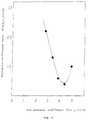
- Figure 7 shows the relationship between the integrated absorption intensity ratio (I 2 /I 1 ) and the electric conductivity and the relationship between the integrated absorption intensity ratio (I 2 /I 1 ) and photo conductivity.
- the integrated absorption intensity ratio (I 2 /I 1 ) is in the range of about 0.2-0.6, the electric conductivity is about 10 -12 s/cm and the photo conductivity is about 10 -6 cm 2 /V, both of which are satisfactory.
- the a-Si layer formed by the electron cyclotron resonance method is advantageous in that: (1) Stable plasma can be produced under relatively low pressure of gas 0.001 to 0.013 Pa (10 -5 -10 -3 Torr) and the production of powdered polymer such as (SiH 2 ) n be avoided by preventing the secondary reaction between the reactants, so that the a-Si layer which is satisfactory can be formed; (2) Because of the high energy of electrons, the efficiencies of decomposition, excitation, and ionization of the introduced gas are remarkably improved. As a result, both the deposition rate and gas availability are increased by 6-10 times.
- the a-Si layer of this invention is suitable for the photosensitive element of a device by which optical information from outside can be converted into electrical signals, so that it can serve as the photoconductive layer of an electrophotographic photosensitive member, the photosensitive element of an image sensor, or the photosensitive element of a liquid crystal or multilayer display device. Moreover, the a-Si layer of this invention can also be applied to various devices such as solar batteries and thin film transistors.
- an electrophotographic photosensitive member 1 to be positively charged as shown in Figure 1 was produced as follows: On a conductive substrate 2, an intermediate layer 3 made of a-Si in which a large amount of boron was doped, a photoconductive layer 4 made of a-Si in which a small amount of boron was doped, and an outer coating layer 5 made of a-SiC were successively formed in that order by the electron cyclotron resonance method.
- a compound of boron with hydrogen or halogen such as B 2 H 6 is preferred.
- an element of Group IIIA of the Periodic Table such as aluminum, gallium, indium, or the like can be used.
- Table 1 The conditions for the production of respective layers are shown in Table 1 below.
- Table 1 Layer MW power (kW) Flow rate Gas pressure Pa SiH 4 (SCCM) B 2 H 6 (SCCM) CH 4 (SLM) Intermediate 2.5 120 30 *1 -- 0.373 Photoconductive 2.5 120 5 *2 -- 0.373 Outer coating 2.5 30 -- 2.0 0.373 *1: 3000 ppm in H 2 . *2: 30 ppm in H 2 .
- the a-Si photoconductive layer 4 contained 48 atomic % of hydrogen, and its absorption coefficient ratio ⁇ (SiH 2 )/ ⁇ (SiH) in the infrared spectrum was 2.15.
- powdered polymer such as (SiH 2 ) n was not produced, and both the deposition rate and the gas availability were increased 6-10 times compared with that of the conventional processes.
- the resulting a-Si type photosensitive member was examined for its properties, its electric-charge retaining property was particularly excellent compared with the conventional a-Si type photosensitive members.
- the a-Si type photosensitive member was used in a commercial copying machine to carry out copying, images of high quality were obtained.
- An electrophotographic photosensitive member 1 as shown in Figure 1 was produced in a similar manner to that of Example 1, except that different gas pressures were used to form the photoconductive layer 4 .
- the resulting photosensitive members were examined for their electric charge retaining property and photosensitivity. The results obtained are shown in Table 2 .
- Table 2 Sample No. 1 2 3 4 5 Gas pressure Pa 0.373 0.453 0.506 0.586 0.666 Electric charge retaining property* o o ⁇ ⁇ ⁇ Photosensitivity* o o ⁇ ⁇ ⁇ * o Very good ⁇ Good ⁇ Acceptable for practical use ⁇ Poor
- the amount of hydrogen contained in the photoconductive layer was measured for each photosensitive member. The results were that when the gas pressure to 0.373 to 0.453 Pa (2.8 x 10 -3 -3.4 x 10 -3 Torr) 45-52 atomic % of hydrogen was contained in the photoconductive layer and when the gas pressure was 0.506 to 0.666 Pa (3.8 x 10 -3 -5.0 x 10 -3 Torr), 20-30 atomic % of hydrogen was contained in the photosensitive layer.
- a photosensitive member to be negatively charged as shown in Figure 1 was produced in a similar manner to that of Example 1, except that an a-Si layer doped with a small amount of phosphorus was used as the photoconductive layer 4 and an a-Si layer doped with a great amount of phosphorus was used as the intermediate layer 3.
- a gas of a compound of phosphorus with hydrogen or halogen such as PH 3 , PCl 3 , or PCl 5 is preferred.
- an element of Group VA or Group VIA of the Periodic Table such as nitrogen, antimony, oxygen or the like can be used. The conditions for the production of respective layers are shown in Table 3 below.
- powdered polymer such as (SiH 2 ) n was not produced, and both the deposition rate and the gas availability were much higher than those obtained following the conventional processes. Furthermore, when the resulting a-Si type photosensitive member was examined for its properties, its electric-charge retaining property was particularly excellent. When the a-Si type photosensitive member was used in a commercial copying machine to carry out copying, images of high quality were obtained.
- an electrophotographic photosensitive member 1 as shown in Figure 1 was produced as follows: On a conductive substrate 2 an intermediate layer 3 made of a-SiN in which a large amount of boron was doped, a photoconductive layer 4 made of a-Si in which a small amount of boron was doped, and an outer coating layer 5 made of a-SiC were successively formed in that order by the electron cyclotron resonance method.
- the a-Si layer of the resulting photosensitive member 1 was of p-type. The conditions for the production of respective layers are shown in Table 4 below.
- electrophotographic photosensitive members with different integrated intensity ratios (I 2 /I 1 ) in the infrared spectra were also produced in the same way as above.
- Figure 7 shows the relationship between the integrated absorption intensity ratio (I 2 /I 1 ) and the electric conductivity, and the relationship between the integrated absorption intensity ratio (I 2 /I 1 ) and the photo conductivity.
- Table 5 shows four other properties of the a-Si type photosensitive members A-D with different integrated absorption intensity ratios and the conventional a-Si type photosensitive member E produced by plasma CVD method.
- the a-Si type photosensitive members B and C with the integrated absorption intensity ratios in the range of 0.2-0.6 have excellent sensitivities and the improved electric-charge retaining property compared with the conventional a-Si type photosensitive member E.
- the image formation was conducted by use of these a-Si type photosensitive members B and C , so that images of high quality free from fog were obtained.
- Table 5 also indicates that, although the a-Si type photosensitive members A and D with the integrated absorption intensity ratios outside the range of 0.2-0.6 have the improved electric-charge retaining property, their sensitivities and residual potentials are unsatisfactory, so that these photosensitive members are not suitable for practical use.
- the a-Si layers with the integrated absorption intensity ratio in the range of 0.2-0.3 were quantitatively analyzed, and it was found that the amounts of hydrogen contained in the a-Si layers were 40-50 atomic %. When the a-Si layer contained hydrogen at a percentage in this range, the dark resistivity and photo conductivity of the photosensitive member were particularly satisfactory.
Landscapes
- Physics & Mathematics (AREA)
- General Physics & Mathematics (AREA)
- Chemical & Material Sciences (AREA)
- Inorganic Chemistry (AREA)
- Photoreceptors In Electrophotography (AREA)
Claims (5)
- Elektrophotographisches, lichtempfindliches Element mit einem elektrisch leitenden Substrat (2), einer auf diesem Substrat hergestellten Zwischenschicht (3), einer auf der Zwischenschicht hergestellten photoleitenden Schicht (4) und einer auf der photoleitenden Schicht hergestellten äußeren Überzugsschicht (5);
dadurch gekennzeichnet, dass die photoleitende Schicht (4) aus amorphem Silizium besteht, das 40 oder mehr Atom-% Wasserstoff und/oder Halogen enthält und das durch das Elektronenzykltrotron-Resonanz-Verfahren ohne Erwärmen des Substrats (2) erhalten werden kann, wobei ein Gas verwendet wird, dessen Druck im Bereich von 0,373 bis 0,453 Pa (2,8 x 10⁻³ bis 3,4 x 10⁻³ Torr) liegt, und wobei das Verhältnis aus dem Absorptionskoeffizienten bei ungefähr 2100 cm-1 von SiH2 zum Absorptionskoeffizienten bei ungefähr 2000 cm-1 von SiH im Infrarotspektrum des amorphen Siliziums im Bereich von 1,3 bis 2,5 liegt, und wobei das Verhältnis der integrierten Absorptionsintensität bei ungefähr 840 cm-1 zur integrierten Absorptionsintensität bei ungefähr 880 cm-1 im Infrarotspektrum des amorphen Siliziums im Bereich von 0,2 bis 0,6 liegt. - Elektrophotographisches, lichtempfindliches Element nach Anspruch 1, bei dem die lichtempfindliche Schicht aus amorphem Silizium besteht, das 40 bis 60 Atom-% Wasserstoff und/oder Halogen enthält.
- Elektrophotographisches, lichtempfindliches Element nach Anspruch 2, bei dem die lichtempfindliche Schicht aus amorphem Silizium besteht, das 40 bis 50 Atom-% Wasserstoff und/oder Halogen enthält.
- Elektrophotographisches, lichtempfindliches Element nach Anspruch 1, bei dem die photoleitende Schicht mit einem Element der Gruppe IIIA des Periodensystems als Fremdstoff dotiert ist.
- Elektrophotographisches, lichtempfindliches Element nach Anspruch 1, bei dem die photoleitende Schicht mit einem Element der Gruppe VIA oder der Gruppe VIA des Periodensystems als Fremdstoff dotiert ist.
Applications Claiming Priority (6)
| Application Number | Priority Date | Filing Date | Title |
|---|---|---|---|
| JP82450/88 | 1988-04-04 | ||
| JP8245088 | 1988-04-04 | ||
| JP63107098A JPH087448B2 (ja) | 1988-04-28 | 1988-04-28 | 電子写真感光体の製造方法 |
| JP107098/88 | 1988-04-28 | ||
| JP63164478A JPH0212260A (ja) | 1988-06-30 | 1988-06-30 | 電子写真感光体およびその製造方法 |
| JP164478/88 | 1988-06-30 |
Publications (3)
| Publication Number | Publication Date |
|---|---|
| EP0336700A2 EP0336700A2 (de) | 1989-10-11 |
| EP0336700A3 EP0336700A3 (de) | 1990-11-22 |
| EP0336700B1 true EP0336700B1 (de) | 1997-07-30 |
Family
ID=27303923
Family Applications (1)
| Application Number | Title | Priority Date | Filing Date |
|---|---|---|---|
| EP89303300A Expired - Lifetime EP0336700B1 (de) | 1988-04-04 | 1989-04-04 | Elektrophotographisches lichtempfindliches Element |
Country Status (4)
| Country | Link |
|---|---|
| US (1) | US4971878A (de) |
| EP (1) | EP0336700B1 (de) |
| KR (1) | KR910007719B1 (de) |
| DE (1) | DE68928210T2 (de) |
Families Citing this family (2)
| Publication number | Priority date | Publication date | Assignee | Title |
|---|---|---|---|---|
| US5239397A (en) * | 1989-10-12 | 1993-08-24 | Sharp Kabushiki | Liquid crystal light valve with amorphous silicon photoconductor of amorphous silicon and hydrogen or a halogen |
| JPH03242653A (ja) * | 1990-02-20 | 1991-10-29 | Sharp Corp | 電子写真感光体 |
Family Cites Families (10)
| Publication number | Priority date | Publication date | Assignee | Title |
|---|---|---|---|---|
| US4265991A (en) * | 1977-12-22 | 1981-05-05 | Canon Kabushiki Kaisha | Electrophotographic photosensitive member and process for production thereof |
| GB2018446B (en) * | 1978-03-03 | 1983-02-23 | Canon Kk | Image-forming member for electrophotography |
| US4217374A (en) * | 1978-03-08 | 1980-08-12 | Energy Conversion Devices, Inc. | Amorphous semiconductors equivalent to crystalline semiconductors |
| JPS574172A (en) * | 1980-06-09 | 1982-01-09 | Canon Inc | Light conductive member |
| JPS57158650A (en) * | 1981-03-25 | 1982-09-30 | Minolta Camera Co Ltd | Amorphous silicon photoconductor layer |
| JPS59159167A (ja) * | 1983-03-01 | 1984-09-08 | Zenko Hirose | アモルフアスシリコン膜の形成方法 |
| DE3322782A1 (de) * | 1983-06-24 | 1985-01-03 | Basf Farben + Fasern Ag, 2000 Hamburg | Hitzehaertbare bindemittelmischung |
| DE3506657A1 (de) * | 1984-02-28 | 1985-09-05 | Sharp K.K., Osaka | Photoleitfaehige vorrichtung |
| US4698288A (en) * | 1985-12-19 | 1987-10-06 | Xerox Corporation | Electrophotographic imaging members having a ground plane of hydrogenated amorphous silicon |
| ES2053526T3 (es) * | 1986-02-04 | 1994-08-01 | Canon Kk | Elemento receptor de luz a utilizar en electrofotografia. |
-
1989
- 1989-04-03 US US07/332,775 patent/US4971878A/en not_active Expired - Lifetime
- 1989-04-04 DE DE68928210T patent/DE68928210T2/de not_active Expired - Fee Related
- 1989-04-04 EP EP89303300A patent/EP0336700B1/de not_active Expired - Lifetime
- 1989-04-04 KR KR1019890004485A patent/KR910007719B1/ko not_active Expired
Also Published As
| Publication number | Publication date |
|---|---|
| KR890016427A (ko) | 1989-11-29 |
| EP0336700A3 (de) | 1990-11-22 |
| EP0336700A2 (de) | 1989-10-11 |
| DE68928210D1 (de) | 1997-09-04 |
| DE68928210T2 (de) | 1998-01-29 |
| KR910007719B1 (ko) | 1991-09-30 |
| US4971878A (en) | 1990-11-20 |
Similar Documents
| Publication | Publication Date | Title |
|---|---|---|
| US4532199A (en) | Method of forming amorphous silicon film | |
| JP2003092200A (ja) | 真空処理方法、真空処理装置、半導体装置の製造方法および半導体装置 | |
| US6849123B2 (en) | Plasma processing method and method for manufacturing semiconductor device | |
| US5371380A (en) | Si- and/or Ge-containing non-single crystalline semiconductor film with an average radius of 3.5 A or less as for microvoids contained therein and a microvoid density 1×10.sup.(19) (cm-3) or less | |
| EP0336700B1 (de) | Elektrophotographisches lichtempfindliches Element | |
| JPH081895B2 (ja) | 非晶質シリコン膜の形成方法 | |
| US4769303A (en) | Electrophotographic photosensitive member | |
| US4965164A (en) | Method for producing electrophotographic photoreceptor | |
| US5100749A (en) | Photosensitive member for electrophotography | |
| EP0348843B1 (de) | Lichtempfindliches Element für Elektrophotographie | |
| US5082760A (en) | Method for preparing an electrophotographic photoreceptor having a charge transporting layer containing aluminum oxide | |
| JPH087448B2 (ja) | 電子写真感光体の製造方法 | |
| JPH07117764B2 (ja) | 電子写真感光体の製造方法 | |
| CN1029162C (zh) | 一种电摄影用的光敏器件 | |
| JPH07117763B2 (ja) | 電子写真感光体の製造方法 | |
| JPH07117762B2 (ja) | 電子写真感光体の製造方法 | |
| JPH0212260A (ja) | 電子写真感光体およびその製造方法 | |
| JPH0772804B2 (ja) | 電子写真感光体 | |
| JPH02301769A (ja) | 電子写真感光体 | |
| JPS63273873A (ja) | 電子写真感光体 | |
| JPH0473146B2 (de) | ||
| JPH0380306B2 (de) | ||
| JPS61130956A (ja) | 電子写真感光体 | |
| JPH0647739B2 (ja) | プラズマcvd法による堆積膜形成方法 | |
| JPS63243955A (ja) | 電子写真感光体 |
Legal Events
| Date | Code | Title | Description |
|---|---|---|---|
| PUAI | Public reference made under article 153(3) epc to a published international application that has entered the european phase |
Free format text: ORIGINAL CODE: 0009012 |
|
| 17P | Request for examination filed |
Effective date: 19890412 |
|
| AK | Designated contracting states |
Kind code of ref document: A2 Designated state(s): DE FR GB IT |
|
| PUAL | Search report despatched |
Free format text: ORIGINAL CODE: 0009013 |
|
| AK | Designated contracting states |
Kind code of ref document: A3 Designated state(s): DE FR GB IT |
|
| 17Q | First examination report despatched |
Effective date: 19930615 |
|
| GRAG | Despatch of communication of intention to grant |
Free format text: ORIGINAL CODE: EPIDOS AGRA |
|
| GRAH | Despatch of communication of intention to grant a patent |
Free format text: ORIGINAL CODE: EPIDOS IGRA |
|
| GRAH | Despatch of communication of intention to grant a patent |
Free format text: ORIGINAL CODE: EPIDOS IGRA |
|
| GRAA | (expected) grant |
Free format text: ORIGINAL CODE: 0009210 |
|
| AK | Designated contracting states |
Kind code of ref document: B1 Designated state(s): DE FR GB IT |
|
| REF | Corresponds to: |
Ref document number: 68928210 Country of ref document: DE Date of ref document: 19970904 |
|
| ET | Fr: translation filed | ||
| PLBE | No opposition filed within time limit |
Free format text: ORIGINAL CODE: 0009261 |
|
| STAA | Information on the status of an ep patent application or granted ep patent |
Free format text: STATUS: NO OPPOSITION FILED WITHIN TIME LIMIT |
|
| 26N | No opposition filed | ||
| REG | Reference to a national code |
Ref country code: GB Ref legal event code: IF02 |
|
| PGFP | Annual fee paid to national office [announced via postgrant information from national office to epo] |
Ref country code: GB Payment date: 20040331 Year of fee payment: 16 |
|
| PGFP | Annual fee paid to national office [announced via postgrant information from national office to epo] |
Ref country code: FR Payment date: 20040408 Year of fee payment: 16 |
|
| PGFP | Annual fee paid to national office [announced via postgrant information from national office to epo] |
Ref country code: DE Payment date: 20040415 Year of fee payment: 16 |
|
| PG25 | Lapsed in a contracting state [announced via postgrant information from national office to epo] |
Ref country code: IT Free format text: LAPSE BECAUSE OF NON-PAYMENT OF DUE FEES;WARNING: LAPSES OF ITALIAN PATENTS WITH EFFECTIVE DATE BEFORE 2007 MAY HAVE OCCURRED AT ANY TIME BEFORE 2007. THE CORRECT EFFECTIVE DATE MAY BE DIFFERENT FROM THE ONE RECORDED. Effective date: 20050404 Ref country code: GB Free format text: LAPSE BECAUSE OF NON-PAYMENT OF DUE FEES Effective date: 20050404 |
|
| PG25 | Lapsed in a contracting state [announced via postgrant information from national office to epo] |
Ref country code: DE Free format text: LAPSE BECAUSE OF NON-PAYMENT OF DUE FEES Effective date: 20051101 |
|
| GBPC | Gb: european patent ceased through non-payment of renewal fee |
Effective date: 20050404 |
|
| PG25 | Lapsed in a contracting state [announced via postgrant information from national office to epo] |
Ref country code: FR Free format text: LAPSE BECAUSE OF NON-PAYMENT OF DUE FEES Effective date: 20051230 |
|
| REG | Reference to a national code |
Ref country code: FR Ref legal event code: ST Effective date: 20051230 |