EP0336700B1 - An electrophotographic photosensitive member - Google Patents
An electrophotographic photosensitive member Download PDFInfo
- Publication number
- EP0336700B1 EP0336700B1 EP89303300A EP89303300A EP0336700B1 EP 0336700 B1 EP0336700 B1 EP 0336700B1 EP 89303300 A EP89303300 A EP 89303300A EP 89303300 A EP89303300 A EP 89303300A EP 0336700 B1 EP0336700 B1 EP 0336700B1
- Authority
- EP
- European Patent Office
- Prior art keywords
- layer
- photosensitive member
- sih
- electrophotographic photosensitive
- gas
- Prior art date
- Legal status (The legal status is an assumption and is not a legal conclusion. Google has not performed a legal analysis and makes no representation as to the accuracy of the status listed.)
- Expired - Lifetime
Links
Images


Classifications
-
- G—PHYSICS
- G03—PHOTOGRAPHY; CINEMATOGRAPHY; ANALOGOUS TECHNIQUES USING WAVES OTHER THAN OPTICAL WAVES; ELECTROGRAPHY; HOLOGRAPHY
- G03G—ELECTROGRAPHY; ELECTROPHOTOGRAPHY; MAGNETOGRAPHY
- G03G5/00—Recording-members for original recording by exposure, e.g. to light, to heat or to electrons; Manufacture thereof; Selection of materials therefor
- G03G5/02—Charge-receiving layers
- G03G5/04—Photoconductive layers; Charge-generation layers or charge-transporting layers; Additives therefor; Binders therefor
- G03G5/08—Photoconductive layers; Charge-generation layers or charge-transporting layers; Additives therefor; Binders therefor characterised by the photoconductive material being inorganic
- G03G5/082—Photoconductive layers; Charge-generation layers or charge-transporting layers; Additives therefor; Binders therefor characterised by the photoconductive material being inorganic and not being incorporated in a bonding material, e.g. vacuum deposited
- G03G5/08214—Silicon-based
- G03G5/08278—Depositing methods
-
- G—PHYSICS
- G03—PHOTOGRAPHY; CINEMATOGRAPHY; ANALOGOUS TECHNIQUES USING WAVES OTHER THAN OPTICAL WAVES; ELECTROGRAPHY; HOLOGRAPHY
- G03G—ELECTROGRAPHY; ELECTROPHOTOGRAPHY; MAGNETOGRAPHY
- G03G5/00—Recording-members for original recording by exposure, e.g. to light, to heat or to electrons; Manufacture thereof; Selection of materials therefor
- G03G5/02—Charge-receiving layers
- G03G5/04—Photoconductive layers; Charge-generation layers or charge-transporting layers; Additives therefor; Binders therefor
- G03G5/08—Photoconductive layers; Charge-generation layers or charge-transporting layers; Additives therefor; Binders therefor characterised by the photoconductive material being inorganic
- G03G5/082—Photoconductive layers; Charge-generation layers or charge-transporting layers; Additives therefor; Binders therefor characterised by the photoconductive material being inorganic and not being incorporated in a bonding material, e.g. vacuum deposited
- G03G5/08214—Silicon-based
- G03G5/08221—Silicon-based comprising one or two silicon based layers
Definitions
- This invention relates to an electrophotographic photosensitive member comprising a photoconductive layer made of amorphous silicon which is formed by an electron cyclotron resonance method.
- U.K. Patent Application GB 2,077,451A relates to a photoconductive member comprising a substrate, a a-Si photoconductive layer, and a barrier layer between the substrate and the photoconductive layer.
- U.S. Patent No. 4,532,199 corresponding to DE-A-3 407 643 relates to a method of forming an amorphous silicon film including the steps of bringing a gas which is pre-excited by electron cyclotron resonance generated by an alternating electric field and a magnetic field into contact with a raw material gas containing silicone atoms in a reaction chamber in which a substrate is placed, so that the raw material gas is converted to radicals, and forming an amorphous silicon film on a surface of the substrate by the reaction of radicals therewith.
- U.S. Patent No. 4,698,288 relates to a photoresponsive imaging member comprising a supporting substrate, a ground plane of hydrogenated silicon having incorporated therein dopants; and a photoconductive layer comprising hydrogenated amorph
- a-Si type photosensitive members have usually been produced by plasma CVD, sputtering, or other techniques.
- a source gas such as monosilane or disilane is first introduced into a vacuum chamber in which a conductive substrate made of aluminum or the like is disposed.
- the introduction of the source gas into the vacuum chamber is followed by glow discharge with the application of high-frequency power, so that the source gas in the vacuum chamber is decomposed and an a-Si layer containing hydrogen is grown on the substrate.
- both H 2 gas and a rare gas such as Ar, He, or the like are first introduced into a chamber, and then glow discharge is caused by the application of high-frequency power, so that the target is sputtered and an a-Si layer containing hydrogen is grown on a substrate.
- the conductive substrate must be heated to form the a-Si layer thereon. Consequently, the amount of hydrogen contained in the a-Si layer is increased.
- the excessive amount of hydrogen contained in the a-Si layer makes its electric conductivity as high as 10 -10 s/cm, so that the electric-charge retaining property of the a-Si layer is deteriorated.
- the electric conductivity of the a-Si layer can be increased by the addition of boron thereto with the use of, for example, B 2 H 6 gas. In this case, however, the degree of increase is relatively small and there can only be obtained the electric conductivity of at most about 10 -11 -10 -12 s/cm.
- the conventional production processes are also disadvantageous in that the deposition rate is very low; the availability of source gas is low; and plenty of powdered polymer such as (SiH 2 ) n is produced as a by-product and deposited on the surface of the conductive substrate during the growth of a-Si layer, so that many defects can be generated in the a-Si layer, resulting in reduced production yield of a-Si type photosensitive members.
- the amount of hydrogen contained in the a-Si layer is strictly limited to the range of 10-40 atomic %.
- Japanese Patent Publication No. 60-35059 and U.S. Patent No. 4,265,991. discloses an a-Si layer containing 10-40 atomic % of hydrogen, in which the ratio of the absorption coefficient ⁇ (SiH 2 ) at around 2100 cm -1 to the absorption coefficient ⁇ (SiH) at around 2000 cm -1 in the infrared spectrum of the a-Si layer is in the range of about 0.2-1.7.
- the absorption coefficient ⁇ (SiH 2 ) at around 2100 cm -1 is due to Si-H 2 bonds
- the absorption coefficient ⁇ (SiH) at around 2000 cm -1 is due to Si-H bonds.
- their resistivity becomes as small as 10 9 ⁇ cm
- boron (B) is doped in the a-Si layer their resistivity is still as small as 10 11 ⁇ cm, so that the electric-charge retaining property of the a-Si type photosensitive members is inferior to that of conventional selenium or organic photosensitive members.
- an electrophotographic photosensitive member comprising an electrically conductive substrate, an intermediate layer formed on said substrate, a photoconductive layer formed on said intermediate layer and an outer coating layer formed on said photoconductive layer, wherein said photoconductive layer is made of amorphous silicon containing 40 or more atomic % of hydrogen and/or halogen, and which is obtainable by the electron cyclotron resonance method without heating the substrate and using a gas pressure in the range from 0.373 to 0.453 Pa (2.8x10 -3 to 3.4x10 -3 Torr), and wherein the ratio of the adsorption coefficient at around 2,100 cm -1 of SiH 2 to the absorption coefficient at around 2,000 cm -1 of SiH in the infrared spectrum of said amorphous silicon is in a range from 1.3 to 2.5, and the ratio of the integrated absorption intensity at around 840 cm -1 to the integrated absorption intensity at around 880 cm -1 in the infrared spectrum of said amorphous silicon is in a range from 0.2
- the photosensitive layer is made of amorphous silicon containing 40 to 60 atomic % of hydrogen and/or halogen.
- the photosensitive layer is made of amorphous silicon containing 40 to 50 atomic % of hydrogen and/or halogen.
- the photoconductive layer is doped with an element of Group IIIA of the Periodic Table as an impurity.
- the photoconductive layer is doped with an element of Group VA or Group VIA of the Periodic Table as an impurity.
- the invention described herein makes possible the provision of (1) an electrophotographic photosensitive member which has high photosensitivity and extremely high dark resistivity, so that its excellent electric-charge retaining property can be attained, resulting in an image of high quality; (2) an electrophotographic photosensitive member which has improved electric conductivity and electric-charge retaining property, so that an image of high quality can be obtained; (3) an electrophotographic photosensitive member which is produced by the electron cyclotron resonance method, so that the deposition rate and gas availability can be improved, resulting in reduced production cost; and (4) an electrophotographic photosensitive member which is produced by the electron cyclotron resonance method, so that the production of powdered polymer such as (SiH 2 ) n can be prevented, resulting in improved production yield.
- the apparatus comprises a plasma formation chamber 11 in which hydrogen plasma is formed and a deposition chamber 12 in which each layer is formed.
- the plasma formation chamber 11 and the deposition chamber 12 which communicate with each other via a plasma inlet 13 , are evacuated with an exhaust system (not shown) comprising an oil diffusion pump and an oil rotary pump.
- the plasma formation chamber 11 serves as a cavity resonator into which 2.45-GHz microwaves are introduced through a waveguide 14 .
- a microwave supply window 15 is made of a quartz glass plate which can transmit the microwaves.
- the plasma formation chamber 11 is provided with a gas supply pipe 19 through which hydrogen gas can be introduced thereinto.
- Magnetic coils 16 and 17 are disposed around the plasma formation chamber 11 .
- the magnetic coil 16 generates a magnetic field (875G) for the formation of plasma and the magnetic coil 17 generates a magnetic field by which the plasma formed in the plasma formation chamber 11 is introduced into the deposition chamber 12 .
- the electrophotographic photosensitive member of this invention is produced with this apparatus as follows: First, a conductive substrate 18 is positioned nearly in the central portion of the deposition chamber 12 .
- the conductive substrate 18 can be, for example, a drum made of aluminum.
- the plasma formation chamber 11 and the deposition chamber 12 are evacuated with the exhaust system. Then, hydrogen gas and, if required, additional gas are introduced into the plasma formation chamber 11 through the gas supply pipe 19 , while source gas is introduced into the deposition chamber 12 through gas supply pipes 20 .
- the source gas can be a gas of silicon compounds such as SiH 4 , Si 2 H 6 , SiF 4 , SiCl 4 , SiHCl 3 , and SiH 2 Cl 2 , or a mixture thereof.
- a-SiC or a-SiN layer is formed, for example, CH 4 or NO gas is added to the source gas.
- the pressure of gas is controlled to be in the order of 0.133 to 0.013 Pa (10 -3 -10 -4 Torr).
- the microwaves generated from a microwave oscillator (not shown) are introduced into the plasma formation chamber 11 , while the magnetic field is being formed.
- the hydrogen gas is converted into plasma in the plasma formation chamber 11 , and the resulting hydrogen plasma is introduced into the deposition chamber 12 through the plasma inlet 13 , to convert the source gas into plasma there.
- the resulting plasma of the source gas is then brought onto the conductive substrate 18 by the magnetic field for the introduction of plasma, and a-Si is deposited on the surface of the conductive substrate 18 .
- a layer e.g., an a-Si layer
- the uniformity of the thickness of the layer can be further improved by regulating the position and size of the plasma inlet 13 .
- the conductivity type of the a-Si layer formed can be determined by the sort of additional gas to be introduced.
- the additional gas of a compound containing an element of Group IIIA of the Periodic Table such as B 2 H 6 or BH 3
- the a-Si layer of p-type is obtained.
- the additional gas of a compound containing an element of Group VA or Group VIA of the Periodic Table such as PH 3 , PCl 3 , or PCl 5 is used, the a-Si layer of n-type is obtained.
- the amount of hydrogen contained in the a-Si layer is 40-60 atomic %, and more preferably 40-50 atomic %.
- the amount of hydrogen contained in the a-Si layer is greater than 60 atomic %, the optical band gap of the a-Si layer becomes excessively large, so that the layer is not suitable for the photoconductive layer of the electrophotographic photosensitive member which must have photosensitivity to visible light.
- the absorption peak due to Si-H bonds is observed at around 2000 cm -1 and the absorption peak due to Si-H 2 bonds is observed at around 800-900 cm -1 in the infrared spectrum of a-Si.
- SiH 2 is present in the form of a monomer
- its absorption peak is observed only at around 880 cm -1
- SiH 2 is present in the form of a polymer such as (SiH 2 ) n
- its absorption peaks are observed both at around 880 cm -1 and at around 840 cm -1 in the infrared spectrum of a-Si.
- SiH 2 and (SiH 2 ) n are present as a mixture, and it is well known that the properties of the photosensitive member such as electric conductivity can vary depending on the ratio of (SiH 2 ) n to SiH 2 .
- the inventors have found that the ratio of (SiH 2 ) n to SiH 2 can be estimated on the basis of the I 2 (the integrated absorption intensity at around 840 cm -1 )/I 1 (the integrated absorption intensity at around 880 cm -1 ) ratio in the infrared spectrum of a-Si.
- the integrated absorption intensity is expressed by the integral ⁇ ⁇ (w)/w ⁇ dw where ⁇ (w) is the absorption coefficient at the wave number of w. If the ratio is nearly set to satisfy the inequality 0.2 ⁇ (I 2 /I 1 ) ⁇ 0.6, it is possible to improve the properties of the a-Si type photosensitive member such as electric conductivity.
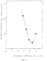
- Figure 7 shows the relationship between the integrated absorption intensity ratio (I 2 /I 1 ) and the electric conductivity and the relationship between the integrated absorption intensity ratio (I 2 /I 1 ) and photo conductivity.
- the integrated absorption intensity ratio (I 2 /I 1 ) is in the range of about 0.2-0.6, the electric conductivity is about 10 -12 s/cm and the photo conductivity is about 10 -6 cm 2 /V, both of which are satisfactory.
- the a-Si layer formed by the electron cyclotron resonance method is advantageous in that: (1) Stable plasma can be produced under relatively low pressure of gas 0.001 to 0.013 Pa (10 -5 -10 -3 Torr) and the production of powdered polymer such as (SiH 2 ) n be avoided by preventing the secondary reaction between the reactants, so that the a-Si layer which is satisfactory can be formed; (2) Because of the high energy of electrons, the efficiencies of decomposition, excitation, and ionization of the introduced gas are remarkably improved. As a result, both the deposition rate and gas availability are increased by 6-10 times.
- the a-Si layer of this invention is suitable for the photosensitive element of a device by which optical information from outside can be converted into electrical signals, so that it can serve as the photoconductive layer of an electrophotographic photosensitive member, the photosensitive element of an image sensor, or the photosensitive element of a liquid crystal or multilayer display device. Moreover, the a-Si layer of this invention can also be applied to various devices such as solar batteries and thin film transistors.
- an electrophotographic photosensitive member 1 to be positively charged as shown in Figure 1 was produced as follows: On a conductive substrate 2, an intermediate layer 3 made of a-Si in which a large amount of boron was doped, a photoconductive layer 4 made of a-Si in which a small amount of boron was doped, and an outer coating layer 5 made of a-SiC were successively formed in that order by the electron cyclotron resonance method.
- a compound of boron with hydrogen or halogen such as B 2 H 6 is preferred.
- an element of Group IIIA of the Periodic Table such as aluminum, gallium, indium, or the like can be used.
- Table 1 The conditions for the production of respective layers are shown in Table 1 below.
- Table 1 Layer MW power (kW) Flow rate Gas pressure Pa SiH 4 (SCCM) B 2 H 6 (SCCM) CH 4 (SLM) Intermediate 2.5 120 30 *1 -- 0.373 Photoconductive 2.5 120 5 *2 -- 0.373 Outer coating 2.5 30 -- 2.0 0.373 *1: 3000 ppm in H 2 . *2: 30 ppm in H 2 .
- the a-Si photoconductive layer 4 contained 48 atomic % of hydrogen, and its absorption coefficient ratio ⁇ (SiH 2 )/ ⁇ (SiH) in the infrared spectrum was 2.15.
- powdered polymer such as (SiH 2 ) n was not produced, and both the deposition rate and the gas availability were increased 6-10 times compared with that of the conventional processes.
- the resulting a-Si type photosensitive member was examined for its properties, its electric-charge retaining property was particularly excellent compared with the conventional a-Si type photosensitive members.
- the a-Si type photosensitive member was used in a commercial copying machine to carry out copying, images of high quality were obtained.
- An electrophotographic photosensitive member 1 as shown in Figure 1 was produced in a similar manner to that of Example 1, except that different gas pressures were used to form the photoconductive layer 4 .
- the resulting photosensitive members were examined for their electric charge retaining property and photosensitivity. The results obtained are shown in Table 2 .
- Table 2 Sample No. 1 2 3 4 5 Gas pressure Pa 0.373 0.453 0.506 0.586 0.666 Electric charge retaining property* o o ⁇ ⁇ ⁇ Photosensitivity* o o ⁇ ⁇ ⁇ * o Very good ⁇ Good ⁇ Acceptable for practical use ⁇ Poor
- the amount of hydrogen contained in the photoconductive layer was measured for each photosensitive member. The results were that when the gas pressure to 0.373 to 0.453 Pa (2.8 x 10 -3 -3.4 x 10 -3 Torr) 45-52 atomic % of hydrogen was contained in the photoconductive layer and when the gas pressure was 0.506 to 0.666 Pa (3.8 x 10 -3 -5.0 x 10 -3 Torr), 20-30 atomic % of hydrogen was contained in the photosensitive layer.
- a photosensitive member to be negatively charged as shown in Figure 1 was produced in a similar manner to that of Example 1, except that an a-Si layer doped with a small amount of phosphorus was used as the photoconductive layer 4 and an a-Si layer doped with a great amount of phosphorus was used as the intermediate layer 3.
- a gas of a compound of phosphorus with hydrogen or halogen such as PH 3 , PCl 3 , or PCl 5 is preferred.
- an element of Group VA or Group VIA of the Periodic Table such as nitrogen, antimony, oxygen or the like can be used. The conditions for the production of respective layers are shown in Table 3 below.
- powdered polymer such as (SiH 2 ) n was not produced, and both the deposition rate and the gas availability were much higher than those obtained following the conventional processes. Furthermore, when the resulting a-Si type photosensitive member was examined for its properties, its electric-charge retaining property was particularly excellent. When the a-Si type photosensitive member was used in a commercial copying machine to carry out copying, images of high quality were obtained.
- an electrophotographic photosensitive member 1 as shown in Figure 1 was produced as follows: On a conductive substrate 2 an intermediate layer 3 made of a-SiN in which a large amount of boron was doped, a photoconductive layer 4 made of a-Si in which a small amount of boron was doped, and an outer coating layer 5 made of a-SiC were successively formed in that order by the electron cyclotron resonance method.
- the a-Si layer of the resulting photosensitive member 1 was of p-type. The conditions for the production of respective layers are shown in Table 4 below.
- electrophotographic photosensitive members with different integrated intensity ratios (I 2 /I 1 ) in the infrared spectra were also produced in the same way as above.
- Figure 7 shows the relationship between the integrated absorption intensity ratio (I 2 /I 1 ) and the electric conductivity, and the relationship between the integrated absorption intensity ratio (I 2 /I 1 ) and the photo conductivity.
- Table 5 shows four other properties of the a-Si type photosensitive members A-D with different integrated absorption intensity ratios and the conventional a-Si type photosensitive member E produced by plasma CVD method.
- the a-Si type photosensitive members B and C with the integrated absorption intensity ratios in the range of 0.2-0.6 have excellent sensitivities and the improved electric-charge retaining property compared with the conventional a-Si type photosensitive member E.
- the image formation was conducted by use of these a-Si type photosensitive members B and C , so that images of high quality free from fog were obtained.
- Table 5 also indicates that, although the a-Si type photosensitive members A and D with the integrated absorption intensity ratios outside the range of 0.2-0.6 have the improved electric-charge retaining property, their sensitivities and residual potentials are unsatisfactory, so that these photosensitive members are not suitable for practical use.
- the a-Si layers with the integrated absorption intensity ratio in the range of 0.2-0.3 were quantitatively analyzed, and it was found that the amounts of hydrogen contained in the a-Si layers were 40-50 atomic %. When the a-Si layer contained hydrogen at a percentage in this range, the dark resistivity and photo conductivity of the photosensitive member were particularly satisfactory.
Landscapes
- Physics & Mathematics (AREA)
- General Physics & Mathematics (AREA)
- Chemical & Material Sciences (AREA)
- Inorganic Chemistry (AREA)
- Photoreceptors In Electrophotography (AREA)
Description
- This invention relates to an electrophotographic photosensitive member comprising a photoconductive layer made of amorphous silicon which is formed by an electron cyclotron resonance method.
- In recent years, as an electrophotographic photosensitive member which is used, for example, in an apparatus for forming images based on electrophotography, there has been proposed a photosensitive member in which a photoconductive layer made of amorphous silicon (referred to as a-Si hereinafter) is formed on a conductive substrate. This a-Si type photosensitive member has numerous advantages such as its long working life, high photosensitivity, high degree of hardness (Hv:1500-2000 kg/mm2), and harmlessness to human bodies. Thus, many attempts have been made to put it into practical use as a desirable photosensitive material.
- U.K. Patent Application GB 2,077,451A relates to a photoconductive member comprising a substrate, a a-Si photoconductive layer, and a barrier layer between the substrate and the photoconductive layer. U.S. Patent No. 4,532,199 corresponding to DE-A-3 407 643 relates to a method of forming an amorphous silicon film including the steps of bringing a gas which is pre-excited by electron cyclotron resonance generated by an alternating electric field and a magnetic field into contact with a raw material gas containing silicone atoms in a reaction chamber in which a substrate is placed, so that the raw material gas is converted to radicals, and forming an amorphous silicon film on a surface of the substrate by the reaction of radicals therewith. U.S. Patent No. 4,698,288 relates to a photoresponsive imaging member comprising a supporting substrate, a ground plane of hydrogenated silicon having incorporated therein dopants; and a photoconductive layer comprising hydrogenated amorphous silicon.
- Conventional a-Si type photosensitive members have usually been produced by plasma CVD, sputtering, or other techniques. In the plasma CVD method, a source gas such as monosilane or disilane is first introduced into a vacuum chamber in which a conductive substrate made of aluminum or the like is disposed. The introduction of the source gas into the vacuum chamber is followed by glow discharge with the application of high-frequency power, so that the source gas in the vacuum chamber is decomposed and an a-Si layer containing hydrogen is grown on the substrate. In the sputtering method, which employs a Si wafer as a target, both H2 gas and a rare gas such as Ar, He, or the like are first introduced into a chamber, and then glow discharge is caused by the application of high-frequency power, so that the target is sputtered and an a-Si layer containing hydrogen is grown on a substrate.
- However, to confer sufficient photosensitivity to the a-Si type photosensitive member in the production processes mentioned above, the conductive substrate must be heated to form the a-Si layer thereon. Consequently, the amount of hydrogen contained in the a-Si layer is increased. The excessive amount of hydrogen contained in the a-Si layer makes its electric conductivity as high as 10-10s/cm, so that the electric-charge retaining property of the a-Si layer is deteriorated.
- The electric conductivity of the a-Si layer can be increased by the addition of boron thereto with the use of, for example, B2H6 gas. In this case, however, the degree of increase is relatively small and there can only be obtained the electric conductivity of at most about 10-11-10-12s/cm.
- The conventional production processes are also disadvantageous in that the deposition rate is very low; the availability of source gas is low; and plenty of powdered polymer such as (SiH2)n is produced as a by-product and deposited on the surface of the conductive substrate during the growth of a-Si layer, so that many defects can be generated in the a-Si layer, resulting in reduced production yield of a-Si type photosensitive members.
- For the conventional a-Si type photosensitive members, the amount of hydrogen contained in the a-Si layer is strictly limited to the range of 10-40 atomic %. (See Japanese Patent Publication No. 60-35059 and U.S. Patent No. 4,265,991.) Moreover, Japanese Laid-open Patent Publication No. 57-158650 discloses an a-Si layer containing 10-40 atomic % of hydrogen, in which the ratio of the absorption coefficient α(SiH2) at around 2100 cm-1 to the absorption coefficient α(SiH) at around 2000 cm-1 in the infrared spectrum of the a-Si layer is in the range of about 0.2-1.7. The absorption coefficient α(SiH2) at around 2100 cm-1 is due to Si-H2 bonds, and the absorption coefficient α(SiH) at around 2000 cm-1 is due to Si-H bonds. To ensure sufficient photosensitivity for the electrophotographic photosensitive members comprising an a-Si photoconductive layer, their resistivity becomes as small as 109Ω·cm, and even when boron (B) is doped in the a-Si layer, their resistivity is still as small as 1011Ω·cm, so that the electric-charge retaining property of the a-Si type photosensitive members is inferior to that of conventional selenium or organic photosensitive members.
- To improve the electric-charge retaining property of the conventional a-Si photosensitive members, it is necessary to increase the absorption coefficient ratio α(SiH2)/ α(SiH). However, in the processes by plasma CVD or sputtering, the reaction of the source gas becomes more active with the increase in high-frequency power in forming each layer, so that a lot of powdered polymer such as (SiH2)n is produced. The resulting powdered polymer is deposited on the surface of the substrate of the photosensitive member, which impairs the quality of the photosensitive member obtained.
- It is an object of the present invention to provide an electrophotographic photosensitive member which overcomes the above-discussed and other disadvantages and deficiencies of the prior art.
- In accordance with the present invention there is provided, an electrophotographic photosensitive member comprising an electrically conductive substrate, an intermediate layer formed on said substrate, a photoconductive layer formed on said intermediate layer and an outer coating layer formed on said photoconductive layer, wherein said photoconductive layer is made of amorphous silicon containing 40 or more atomic % of hydrogen and/or halogen, and which is obtainable by the electron cyclotron resonance method without heating the substrate and using a gas pressure in the range from 0.373 to 0.453 Pa (2.8x10⁻³ to 3.4x10⁻³ Torr), and wherein the ratio of the adsorption coefficient at around 2,100 cm-1 of SiH2 to the absorption coefficient at around 2,000 cm-1 of SiH in the infrared spectrum of said amorphous silicon is in a range from 1.3 to 2.5, and the ratio of the integrated absorption intensity at around 840 cm-1 to the integrated absorption intensity at around 880 cm-1 in the infrared spectrum of said amorphous silicon is in a range from 0.2 to 0.6.
- In a preferred embodiment, the photosensitive layer is made of amorphous silicon containing 40 to 60 atomic % of hydrogen and/or halogen.
- In a more preferred embodiment, the photosensitive layer is made of amorphous silicon containing 40 to 50 atomic % of hydrogen and/or halogen.
- In a preferred embodiment, the photoconductive layer is doped with an element of Group IIIA of the Periodic Table as an impurity.
- In a preferred embodiment, the photoconductive layer is doped with an element of Group VA or Group VIA of the Periodic Table as an impurity.
- Thus, the invention described herein makes possible the provision of (1) an electrophotographic photosensitive member which has high photosensitivity and extremely high dark resistivity, so that its excellent electric-charge retaining property can be attained, resulting in an image of high quality; (2) an electrophotographic photosensitive member which has improved electric conductivity and electric-charge retaining property, so that an image of high quality can be obtained; (3) an electrophotographic photosensitive member which is produced by the electron cyclotron resonance method, so that the deposition rate and gas availability can be improved, resulting in reduced production cost; and (4) an electrophotographic photosensitive member which is produced by the electron cyclotron resonance method, so that the production of powdered polymer such as (SiH2)n can be prevented, resulting in improved production yield.
- The invention is described further hereinafter, by way of example only, with reference to the accompanying drawings, in which:
- Figure 1 is a cross sectional view showing the structure of an electrophotographic photosensitive member of this invention;
- Figure 2 is a cross sectional view showing an apparatus for the production of the electrophotographic photosensitive member of this invention by an electron cyclotron resonance method;
- Figure 3 shows the relationship between the pressure of gas and the hydrogen content in the a-Si layers of various electrophotographic photosensitive members;
- Figure 4 shows the relationship between the pressure of gas and the absorption coefficient ratio α(SiH2)/α(SiH) of the a-Si layers of various electrophotographic photosensitive members;
- Figure 5 shows the relationship between the pressure of gas and the photo conductivity (η·µ·τ) of the a-Si layers of various electrophotographic photosensitive members;
- Figure 6 shows the relationship between the pressure of gas and the dark resistivity (ρd) of the a-Si layers of various electrophotographic photosensitive members; and
- Figure 7 shows the relationship between the integrated absorption intensity ratio (I2/I1) and the electric conductivity and the relationship between the integrated absorption intensity ratio (I2/I1) and the photo conductivity (η·µ·τ) of the a-Si layers of various electrophotographic photosensitive members.
- In Figure 2, the apparatus comprises a
plasma formation chamber 11 in which hydrogen plasma is formed and adeposition chamber 12 in which each layer is formed. Theplasma formation chamber 11 and thedeposition chamber 12, which communicate with each other via aplasma inlet 13, are evacuated with an exhaust system (not shown) comprising an oil diffusion pump and an oil rotary pump. - The
plasma formation chamber 11 serves as a cavity resonator into which 2.45-GHz microwaves are introduced through awaveguide 14. Amicrowave supply window 15 is made of a quartz glass plate which can transmit the microwaves. Theplasma formation chamber 11 is provided with agas supply pipe 19 through which hydrogen gas can be introduced thereinto.Magnetic coils plasma formation chamber 11. Themagnetic coil 16 generates a magnetic field (875G) for the formation of plasma and themagnetic coil 17 generates a magnetic field by which the plasma formed in theplasma formation chamber 11 is introduced into thedeposition chamber 12. - The electrophotographic photosensitive member of this invention is produced with this apparatus as follows: First, a
conductive substrate 18 is positioned nearly in the central portion of thedeposition chamber 12. Theconductive substrate 18 can be, for example, a drum made of aluminum. Theplasma formation chamber 11 and thedeposition chamber 12 are evacuated with the exhaust system. Then, hydrogen gas and, if required, additional gas are introduced into theplasma formation chamber 11 through thegas supply pipe 19, while source gas is introduced into thedeposition chamber 12 throughgas supply pipes 20. The source gas can be a gas of silicon compounds such as SiH4, Si2H6, SiF4, SiCl4, SiHCl3, and SiH2Cl2, or a mixture thereof. When an a-SiC or a-SiN layer is formed, for example, CH4 or NO gas is added to the source gas. In this case the pressure of gas is controlled to be in the order of 0.133 to 0.013 Pa (10-3-10-4 Torr). Then the microwaves generated from a microwave oscillator (not shown) are introduced into theplasma formation chamber 11, while the magnetic field is being formed. The hydrogen gas is converted into plasma in theplasma formation chamber 11, and the resulting hydrogen plasma is introduced into thedeposition chamber 12 through theplasma inlet 13, to convert the source gas into plasma there. The resulting plasma of the source gas is then brought onto theconductive substrate 18 by the magnetic field for the introduction of plasma, and a-Si is deposited on the surface of theconductive substrate 18. Because theconductive substrate 18 is being rotated by a supporting member, a layer (e.g., an a-Si layer) having a uniform thickness can be formed on the surface of theconductive substrate 18. The uniformity of the thickness of the layer can be further improved by regulating the position and size of theplasma inlet 13. - As is similar to the case of the conventional plasma CVD, the conductivity type of the a-Si layer formed can be determined by the sort of additional gas to be introduced. When the additional gas of a compound containing an element of Group IIIA of the Periodic Table such as B2H6 or BH3 is used, the a-Si layer of p-type is obtained. On the contrary, when the additional gas of a compound containing an element of Group VA or Group VIA of the Periodic Table such as PH3, PCl3, or PCl5 is used, the a-Si layer of n-type is obtained.
- With this apparatus, a series of experiments for forming a-Si layers were conducted using the source gas of SiH4 under the different pressures of gas. The dependences of the hydrogen content, absorption coefficient ratio α(SiH2)/ α(SiH), photo conductivity (η·µ·τ), and dark resistivity (ρd) of these a-Si layers upon the pressure of gas are respectively shown in Figures 3, 4, 5, and 6.
- As can be seen from these figures, when 40 atomic % or more of hydrogen was contained in the a-Si layer and the absorption coefficient ratio α(SiH2)/ α(SiH) was in the range of 1.3-2.5, the a-Si layer having dark resistivity of 1012Ω·cm or more and high photo conductivity (i.e., high photosensitivity) was obtained. It is noted that the conventional a-Si layers containing 40 atomic % or less of hydrogen and having the ratio α(SiH2)/ α(SiH) in the range of 0.2-1.7 could not have attained dark resistivity of 1012Ω·cm or more and high photo conductivity (i.e., high photosensitivity). Preferably, the amount of hydrogen contained in the a-Si layer is 40-60 atomic %, and more preferably 40-50 atomic %. When the amount of hydrogen contained in the a-Si layer is greater than 60 atomic %, the optical band gap of the a-Si layer becomes excessively large, so that the layer is not suitable for the photoconductive layer of the electrophotographic photosensitive member which must have photosensitivity to visible light.
- In general, the absorption peak due to Si-H bonds is observed at around 2000 cm-1 and the absorption peak due to Si-H2 bonds is observed at around 800-900 cm-1 in the infrared spectrum of a-Si. When SiH2 is present in the form of a monomer, its absorption peak is observed only at around 880 cm-1 and when SiH2 is present in the form of a polymer such as (SiH2)n, its absorption peaks are observed both at around 880 cm-1 and at around 840 cm-1 in the infrared spectrum of a-Si.
- As for the a-Si layer of the electrophotographic photosensitive member, SiH2 and (SiH2)n are present as a mixture, and it is well known that the properties of the photosensitive member such as electric conductivity can vary depending on the ratio of (SiH2)n to SiH2. The inventors have found that the ratio of (SiH2)n to SiH2 can be estimated on the basis of the I2 (the integrated absorption intensity at around 840 cm-1)/I1 (the integrated absorption intensity at around 880 cm-1) ratio in the infrared spectrum of a-Si. The integrated absorption intensity is expressed by the integral ∫ α (w)/w·dw where α (w) is the absorption coefficient at the wave number of w. If the ratio is nearly set to satisfy the inequality 0.2<(I2/I1)<0.6, it is possible to improve the properties of the a-Si type photosensitive member such as electric conductivity.
- Figure 7 shows the relationship between the integrated absorption intensity ratio (I2/I1) and the electric conductivity and the relationship between the integrated absorption intensity ratio (I2/I1) and photo conductivity. When the integrated absorption intensity ratio (I2/I1) is in the range of about 0.2-0.6, the electric conductivity is about 10-12s/cm and the photo conductivity is about 10-6cm2/V, both of which are satisfactory.
- The a-Si layer formed by the electron cyclotron resonance method is advantageous in that: (1) Stable plasma can be produced under relatively low pressure of gas 0.001 to 0.013 Pa (10-5-10-3 Torr) and the production of powdered polymer such as (SiH2)n be avoided by preventing the secondary reaction between the reactants, so that the a-Si layer which is satisfactory can be formed; (2) Because of the high energy of electrons, the efficiencies of decomposition, excitation, and ionization of the introduced gas are remarkably improved. As a result, both the deposition rate and gas availability are increased by 6-10 times. For example, it is possible to attain the deposition rate of about 23 µm/hr and the gas availability of about 49%; and (3) Because of the appropriate degree of ion impingement, it is possible to form the a-Si layer without heating the conductive substrate, so that the amount of (SiH2)n contained in the a-Si layer can be reduced, resulting in a high-quality a-Si layer with high photosensitivity.
- The a-Si layer of this invention is suitable for the photosensitive element of a device by which optical information from outside can be converted into electrical signals, so that it can serve as the photoconductive layer of an electrophotographic photosensitive member, the photosensitive element of an image sensor, or the photosensitive element of a liquid crystal or multilayer display device. Moreover, the a-Si layer of this invention can also be applied to various devices such as solar batteries and thin film transistors.
- In this example, an electrophotographic
photosensitive member 1 to be positively charged as shown in Figure 1 was produced as follows: On aconductive substrate 2, anintermediate layer 3 made of a-Si in which a large amount of boron was doped, aphotoconductive layer 4 made of a-Si in which a small amount of boron was doped, and anouter coating layer 5 made of a-SiC were successively formed in that order by the electron cyclotron resonance method. As an additional gas for doping boron in the a-Si layers, a compound of boron with hydrogen or halogen such as B2H6 is preferred. In place of boron, an element of Group IIIA of the Periodic Table such as aluminum, gallium, indium, or the like can be used. The conditions for the production of respective layers are shown in Table 1 below.Table 1 Layer MW power (kW) Flow rate Gas pressure Pa SiH4 (SCCM) B2H6 (SCCM) CH4 (SLM) Intermediate 2.5 120 30 *1 -- 0.373 Photoconductive 2.5 120 5 *2 -- 0.373 Outer coating 2.5 30 -- 2.0 0.373 *1: 3000 ppm in H2. *2: 30 ppm in H2. - The
a-Si photoconductive layer 4 contained 48 atomic % of hydrogen, and its absorption coefficient ratio α(SiH2)/α(SiH) in the infrared spectrum was 2.15. - In this example, powdered polymer such as (SiH2)n was not produced, and both the deposition rate and the gas availability were increased 6-10 times compared with that of the conventional processes. Moreover, when the resulting a-Si type photosensitive member was examined for its properties, its electric-charge retaining property was particularly excellent compared with the conventional a-Si type photosensitive members. When the a-Si type photosensitive member was used in a commercial copying machine to carry out copying, images of high quality were obtained.
- When an a-SiN layer or a-SiO layer formed by the electron cyclotron resonance method was used as the
outer coating layer 5 instead of the a-SiC layer, the results obtained were also satisfactory. - An electrophotographic
photosensitive member 1 as shown in Figure 1 was produced in a similar manner to that of Example 1, except that different gas pressures were used to form thephotoconductive layer 4. The resulting photosensitive members were examined for their electric charge retaining property and photosensitivity. The results obtained are shown in Table 2.Table 2 Sample No. 1 2 3 4 5 Gas pressure Pa 0.373 0.453 0.506 0.586 0.666 Electric charge retaining property* ⓞ ⓞ ○ Δ Δ Photosensitivity* ⓞ ⓞ × × × * ⓞ Very good
○ Good
Δ Acceptable for practical use
× Poor - As can be seen from Table 2 above, satisfactory results were obtained when the ratio α(SiH2)/α(SiH) was set to 1.3-2.5 by controlling the gas pressure to 0.373 to 0.453 Pa (2.8 x 10⁻³-3.4 x10⁻³ Torr) according to the relationship shown in Figure 4.
- The amount of hydrogen contained in the photoconductive layer was measured for each photosensitive member. The results were that when the gas pressure to 0.373 to 0.453 Pa (2.8 x 10⁻³-3.4 x 10⁻³ Torr) 45-52 atomic % of hydrogen was contained in the photoconductive layer and when the gas pressure was 0.506 to 0.666 Pa (3.8 x 10⁻³-5.0 x 10⁻³ Torr), 20-30 atomic % of hydrogen was contained in the photosensitive layer.
- A photosensitive member to be negatively charged as shown in Figure 1 was produced in a similar manner to that of Example 1, except that an a-Si layer doped with a small amount of phosphorus was used as the
photoconductive layer 4 and an a-Si layer doped with a great amount of phosphorus was used as theintermediate layer 3. As an additional gas for doping phosphorus in the a-Si layers, a gas of a compound of phosphorus with hydrogen or halogen such as PH3, PCl3, or PCl5 is preferred. In place of phosphorus, an element of Group VA or Group VIA of the Periodic Table such as nitrogen, antimony, oxygen or the like can be used. The conditions for the production of respective layers are shown in Table 3 below.Table 3 Layer MW power (kW) Flow rate Gas pressure Pa SiH4 (SCCM) PH3 (SCCM) CH4 (SLM) *1 Intermediate 2.5 120 10 -- 0.373 *2 Photoconductive 2.5 120 1 -- 0.373 Outer coating 2.5 30 -- 2.0 0.373 *1: 3000 ppm in H2. *2: 30 ppm in H2. - In this example, powdered polymer such as (SiH2)n was not produced, and both the deposition rate and the gas availability were much higher than those obtained following the conventional processes. Furthermore, when the resulting a-Si type photosensitive member was examined for its properties, its electric-charge retaining property was particularly excellent. When the a-Si type photosensitive member was used in a commercial copying machine to carry out copying, images of high quality were obtained.
- When an a-SiN layer or a-SiO layer formed by the electron cyclotron resonance method was used as the
outer coating layer 5 instead of the a-SiC layer, the results obtained were also satisfactory. - In this example, an electrophotographic
photosensitive member 1 as shown in Figure 1 was produced as follows: On aconductive substrate 2 anintermediate layer 3 made of a-SiN in which a large amount of boron was doped, aphotoconductive layer 4 made of a-Si in which a small amount of boron was doped, and anouter coating layer 5 made of a-SiC were successively formed in that order by the electron cyclotron resonance method. The a-Si layer of the resultingphotosensitive member 1 was of p-type. The conditions for the production of respective layers are shown in Table 4 below.Table 4 Layer*1 MW power (kW) Flow rate Gas pressure Pa SiH4 (SCCM) B2H6 (SCCM) NO (SCCM) CH4 (SCCM) *2 Intermediate 2.5 120 22 12 -- 0.359 *3 Photosensitive 2.5 120 6 -- -- 0.359 Outer coating 1.5 120 -- -- 18 0.106 *1: The substrate was at room temperature. *2: 3000 ppm in H2. *3: 30 ppm in H2. - In this example, electrophotographic photosensitive members with different integrated intensity ratios (I2/I1) in the infrared spectra were also produced in the same way as above. Figure 7 shows the relationship between the integrated absorption intensity ratio (I2/I1) and the electric conductivity, and the relationship between the integrated absorption intensity ratio (I2/I1) and the photo conductivity. Table 5 shows four other properties of the a-Si type photosensitive members A-D with different integrated absorption intensity ratios and the conventional a-Si type photosensitive member E produced by plasma CVD method.
Table 5 Sample A B C D E Surface potential(V) 870 860 860 800 820 Percentage of electric charge remaining 1 second after charging (%) 89 89 88 83 79 Sensitivity (cm2/erg) 0.1 0.42 0.44 0.23 0.45 Residual Potential (V) 210 50 45 105 35 - The a-Si type photosensitive members B and C with the integrated absorption intensity ratios in the range of 0.2-0.6 have excellent sensitivities and the improved electric-charge retaining property compared with the conventional a-Si type photosensitive member E. The image formation was conducted by use of these a-Si type photosensitive members B and C, so that images of high quality free from fog were obtained. Table 5 also indicates that, although the a-Si type photosensitive members A and D with the integrated absorption intensity ratios outside the range of 0.2-0.6 have the improved electric-charge retaining property, their sensitivities and residual potentials are unsatisfactory, so that these photosensitive members are not suitable for practical use.
- The a-Si layers with the integrated absorption intensity ratio in the range of 0.2-0.3 were quantitatively analyzed, and it was found that the amounts of hydrogen contained in the a-Si layers were 40-50 atomic %. When the a-Si layer contained hydrogen at a percentage in this range, the dark resistivity and photo conductivity of the photosensitive member were particularly satisfactory.
- It is understood that various other modifications will be apparent to and can be readily made by those skilled in the art without departing from the scope of this invention as defined by the appended claims.
Claims (5)
- An electrophotographic photosensitive member comprising an electrically conductive substrate (2), an intermediate layer (3) formed on said substrate, a photoconductive layer (4) formed on said intermediate layer and an outer coating layer (5) formed on said photoconductive layer,
characterized in that said photoconductive layer (4) is made of amorphous silicon containing 40 or more atomic % of hydrogen and/or halogen, and which is obtainable by the electron cyclotron resonance method without heating the substrate (2) and using a gas whose pressure is in the range from 0.373 to 0.453 Pa (2.8x10⁻³ to 3.4x10⁻³ Torr), and wherein the ratio of the absorption coefficient at around 2,100 cm-1 of SiH2 to the absorption coefficient at around 2,000 cm-1 of SiH in the infrared spectrum of said amorphous silicon is in a range from 1.3 to 2.5, and the ratio of the integrated absorption intensity at around 840 cm-1 to the integrated absorption intensity at around 880 cm-1 in the infrared spectrum of said amorphous silicon is in a range from 0.2 to 0.6. - An electrophotographic photosensitive member according to claim 1, wherein said photosensitive layer is made of amorphous silicon containing 40 to 60 atomic % of hydrogen and/or halogen.
- An electrophotographic photosensitive member according to claim 2, wherein said photosensitive layer is made of amorphous silicon containing 40 to 50 atomic % of hydrogen and/or halogen.
- An electrophotographic photosensitive member according to claim 1, wherein said photoconductive layer is doped with an element of Group IIIA of the Periodic Table as an impurity.
- An electrophotographic photosensitive member according to claim 1, wherein said photoconductive layer is doped with an element of Group VA or Group VIA of the Periodic Table as an impurity.
Applications Claiming Priority (6)
| Application Number | Priority Date | Filing Date | Title |
|---|---|---|---|
| JP8245088 | 1988-04-04 | ||
| JP82450/88 | 1988-04-04 | ||
| JP107098/88 | 1988-04-28 | ||
| JP63107098A JPH087448B2 (en) | 1988-04-28 | 1988-04-28 | Method for manufacturing electrophotographic photoreceptor |
| JP63164478A JPH0212260A (en) | 1988-06-30 | 1988-06-30 | Electrophotographic sensitive body and production of same |
| JP164478/88 | 1988-06-30 |
Publications (3)
| Publication Number | Publication Date |
|---|---|
| EP0336700A2 EP0336700A2 (en) | 1989-10-11 |
| EP0336700A3 EP0336700A3 (en) | 1990-11-22 |
| EP0336700B1 true EP0336700B1 (en) | 1997-07-30 |
Family
ID=27303923
Family Applications (1)
| Application Number | Title | Priority Date | Filing Date |
|---|---|---|---|
| EP89303300A Expired - Lifetime EP0336700B1 (en) | 1988-04-04 | 1989-04-04 | An electrophotographic photosensitive member |
Country Status (4)
| Country | Link |
|---|---|
| US (1) | US4971878A (en) |
| EP (1) | EP0336700B1 (en) |
| KR (1) | KR910007719B1 (en) |
| DE (1) | DE68928210T2 (en) |
Families Citing this family (2)
| Publication number | Priority date | Publication date | Assignee | Title |
|---|---|---|---|---|
| US5239397A (en) * | 1989-10-12 | 1993-08-24 | Sharp Kabushiki | Liquid crystal light valve with amorphous silicon photoconductor of amorphous silicon and hydrogen or a halogen |
| JPH03242653A (en) * | 1990-02-20 | 1991-10-29 | Sharp Corp | electrophotographic photoreceptor |
Family Cites Families (10)
| Publication number | Priority date | Publication date | Assignee | Title |
|---|---|---|---|---|
| AU530905B2 (en) * | 1977-12-22 | 1983-08-04 | Canon Kabushiki Kaisha | Electrophotographic photosensitive member |
| GB2018446B (en) * | 1978-03-03 | 1983-02-23 | Canon Kk | Image-forming member for electrophotography |
| US4217374A (en) * | 1978-03-08 | 1980-08-12 | Energy Conversion Devices, Inc. | Amorphous semiconductors equivalent to crystalline semiconductors |
| JPS574172A (en) * | 1980-06-09 | 1982-01-09 | Canon Inc | Light conductive member |
| JPS57158650A (en) * | 1981-03-25 | 1982-09-30 | Minolta Camera Co Ltd | Amorphous silicon photoconductor layer |
| JPS59159167A (en) * | 1983-03-01 | 1984-09-08 | Zenko Hirose | Manufacture of amorphous silicon film |
| DE3322782A1 (en) * | 1983-06-24 | 1985-01-03 | Basf Farben + Fasern Ag, 2000 Hamburg | HEAT-CURABLE BINDING MIXTURE |
| DE3546544C2 (en) * | 1984-02-28 | 1990-02-15 | Sharp K.K., Osaka, Jp | |
| US4698288A (en) * | 1985-12-19 | 1987-10-06 | Xerox Corporation | Electrophotographic imaging members having a ground plane of hydrogenated amorphous silicon |
| ES2053526T3 (en) * | 1986-02-04 | 1994-08-01 | Canon Kk | LIGHT RECEIVING ELEMENT TO BE USED IN ELECTROPHOTOGRAPHY. |
-
1989
- 1989-04-03 US US07/332,775 patent/US4971878A/en not_active Expired - Lifetime
- 1989-04-04 KR KR1019890004485A patent/KR910007719B1/en not_active Expired
- 1989-04-04 DE DE68928210T patent/DE68928210T2/en not_active Expired - Fee Related
- 1989-04-04 EP EP89303300A patent/EP0336700B1/en not_active Expired - Lifetime
Also Published As
| Publication number | Publication date |
|---|---|
| EP0336700A3 (en) | 1990-11-22 |
| KR890016427A (en) | 1989-11-29 |
| KR910007719B1 (en) | 1991-09-30 |
| EP0336700A2 (en) | 1989-10-11 |
| US4971878A (en) | 1990-11-20 |
| DE68928210T2 (en) | 1998-01-29 |
| DE68928210D1 (en) | 1997-09-04 |
Similar Documents
| Publication | Publication Date | Title |
|---|---|---|
| US4532199A (en) | Method of forming amorphous silicon film | |
| JP2003092200A (en) | Vacuum processing method, vacuum processing apparatus, semiconductor device manufacturing method, and semiconductor device | |
| US6849123B2 (en) | Plasma processing method and method for manufacturing semiconductor device | |
| US5371380A (en) | Si- and/or Ge-containing non-single crystalline semiconductor film with an average radius of 3.5 A or less as for microvoids contained therein and a microvoid density 1×10.sup.(19) (cm-3) or less | |
| EP0336700B1 (en) | An electrophotographic photosensitive member | |
| JPH081895B2 (en) | Method for forming amorphous silicon film | |
| US4769303A (en) | Electrophotographic photosensitive member | |
| US4965164A (en) | Method for producing electrophotographic photoreceptor | |
| US5100749A (en) | Photosensitive member for electrophotography | |
| EP0348843B1 (en) | Photosensitive member for electrophotography | |
| US5082760A (en) | Method for preparing an electrophotographic photoreceptor having a charge transporting layer containing aluminum oxide | |
| JPH087448B2 (en) | Method for manufacturing electrophotographic photoreceptor | |
| JPH07117764B2 (en) | Method for manufacturing electrophotographic photoreceptor | |
| CN1029162C (en) | A photosensitive device for electrophotography | |
| JPH07117763B2 (en) | Method for manufacturing electrophotographic photoreceptor | |
| JPH07117762B2 (en) | Method for manufacturing electrophotographic photoreceptor | |
| JPH0212260A (en) | Electrophotographic sensitive body and production of same | |
| JPH0772804B2 (en) | Electrophotographic photoreceptor | |
| JPH02301769A (en) | Electrophotographic sensitive body | |
| JPS63273873A (en) | Electrophotographic sensitive body | |
| JPH0473146B2 (en) | ||
| JPH0380306B2 (en) | ||
| JPS61130956A (en) | Electrophotographic sensitive body | |
| JPH0647739B2 (en) | Method for forming deposited film by plasma CVD method | |
| JPS63243955A (en) | Electrophotographic sensitive body |
Legal Events
| Date | Code | Title | Description |
|---|---|---|---|
| PUAI | Public reference made under article 153(3) epc to a published international application that has entered the european phase |
Free format text: ORIGINAL CODE: 0009012 |
|
| 17P | Request for examination filed |
Effective date: 19890412 |
|
| AK | Designated contracting states |
Kind code of ref document: A2 Designated state(s): DE FR GB IT |
|
| PUAL | Search report despatched |
Free format text: ORIGINAL CODE: 0009013 |
|
| AK | Designated contracting states |
Kind code of ref document: A3 Designated state(s): DE FR GB IT |
|
| 17Q | First examination report despatched |
Effective date: 19930615 |
|
| GRAG | Despatch of communication of intention to grant |
Free format text: ORIGINAL CODE: EPIDOS AGRA |
|
| GRAH | Despatch of communication of intention to grant a patent |
Free format text: ORIGINAL CODE: EPIDOS IGRA |
|
| GRAH | Despatch of communication of intention to grant a patent |
Free format text: ORIGINAL CODE: EPIDOS IGRA |
|
| GRAA | (expected) grant |
Free format text: ORIGINAL CODE: 0009210 |
|
| AK | Designated contracting states |
Kind code of ref document: B1 Designated state(s): DE FR GB IT |
|
| REF | Corresponds to: |
Ref document number: 68928210 Country of ref document: DE Date of ref document: 19970904 |
|
| ET | Fr: translation filed | ||
| PLBE | No opposition filed within time limit |
Free format text: ORIGINAL CODE: 0009261 |
|
| STAA | Information on the status of an ep patent application or granted ep patent |
Free format text: STATUS: NO OPPOSITION FILED WITHIN TIME LIMIT |
|
| 26N | No opposition filed | ||
| REG | Reference to a national code |
Ref country code: GB Ref legal event code: IF02 |
|
| PGFP | Annual fee paid to national office [announced via postgrant information from national office to epo] |
Ref country code: GB Payment date: 20040331 Year of fee payment: 16 |
|
| PGFP | Annual fee paid to national office [announced via postgrant information from national office to epo] |
Ref country code: FR Payment date: 20040408 Year of fee payment: 16 |
|
| PGFP | Annual fee paid to national office [announced via postgrant information from national office to epo] |
Ref country code: DE Payment date: 20040415 Year of fee payment: 16 |
|
| PG25 | Lapsed in a contracting state [announced via postgrant information from national office to epo] |
Ref country code: IT Free format text: LAPSE BECAUSE OF NON-PAYMENT OF DUE FEES;WARNING: LAPSES OF ITALIAN PATENTS WITH EFFECTIVE DATE BEFORE 2007 MAY HAVE OCCURRED AT ANY TIME BEFORE 2007. THE CORRECT EFFECTIVE DATE MAY BE DIFFERENT FROM THE ONE RECORDED. Effective date: 20050404 Ref country code: GB Free format text: LAPSE BECAUSE OF NON-PAYMENT OF DUE FEES Effective date: 20050404 |
|
| PG25 | Lapsed in a contracting state [announced via postgrant information from national office to epo] |
Ref country code: DE Free format text: LAPSE BECAUSE OF NON-PAYMENT OF DUE FEES Effective date: 20051101 |
|
| GBPC | Gb: european patent ceased through non-payment of renewal fee |
Effective date: 20050404 |
|
| PG25 | Lapsed in a contracting state [announced via postgrant information from national office to epo] |
Ref country code: FR Free format text: LAPSE BECAUSE OF NON-PAYMENT OF DUE FEES Effective date: 20051230 |
|
| REG | Reference to a national code |
Ref country code: FR Ref legal event code: ST Effective date: 20051230 |