EP0335553A2 - Self-scanning light-emitting element array - Google Patents
Self-scanning light-emitting element array Download PDFInfo
- Publication number
- EP0335553A2 EP0335553A2 EP89302751A EP89302751A EP0335553A2 EP 0335553 A2 EP0335553 A2 EP 0335553A2 EP 89302751 A EP89302751 A EP 89302751A EP 89302751 A EP89302751 A EP 89302751A EP 0335553 A2 EP0335553 A2 EP 0335553A2
- Authority
- EP
- European Patent Office
- Prior art keywords
- light
- emitting elements
- array
- emitting
- emitting element
- Prior art date
- Legal status (The legal status is an assumption and is not a legal conclusion. Google has not performed a legal analysis and makes no representation as to the accuracy of the status listed.)
- Granted
Links
Images


Classifications
-
- G—PHYSICS
- G06—COMPUTING OR CALCULATING; COUNTING
- G06K—GRAPHICAL DATA READING; PRESENTATION OF DATA; RECORD CARRIERS; HANDLING RECORD CARRIERS
- G06K15/00—Arrangements for producing a permanent visual presentation of the output data, e.g. computer output printers
- G06K15/02—Arrangements for producing a permanent visual presentation of the output data, e.g. computer output printers using printers
- G06K15/12—Arrangements for producing a permanent visual presentation of the output data, e.g. computer output printers using printers by photographic printing, e.g. by laser printers
- G06K15/1238—Arrangements for producing a permanent visual presentation of the output data, e.g. computer output printers using printers by photographic printing, e.g. by laser printers simultaneously exposing more than one point
- G06K15/1242—Arrangements for producing a permanent visual presentation of the output data, e.g. computer output printers using printers by photographic printing, e.g. by laser printers simultaneously exposing more than one point on one main scanning line
- G06K15/1247—Arrangements for producing a permanent visual presentation of the output data, e.g. computer output printers using printers by photographic printing, e.g. by laser printers simultaneously exposing more than one point on one main scanning line using an array of light sources, e.g. a linear array
-
- B—PERFORMING OPERATIONS; TRANSPORTING
- B41—PRINTING; LINING MACHINES; TYPEWRITERS; STAMPS
- B41J—TYPEWRITERS; SELECTIVE PRINTING MECHANISMS, i.e. MECHANISMS PRINTING OTHERWISE THAN FROM A FORME; CORRECTION OF TYPOGRAPHICAL ERRORS
- B41J2/00—Typewriters or selective printing mechanisms characterised by the printing or marking process for which they are designed
- B41J2/435—Typewriters or selective printing mechanisms characterised by the printing or marking process for which they are designed characterised by selective application of radiation to a printing material or impression-transfer material
- B41J2/447—Typewriters or selective printing mechanisms characterised by the printing or marking process for which they are designed characterised by selective application of radiation to a printing material or impression-transfer material using arrays of radiation sources
- B41J2/45—Typewriters or selective printing mechanisms characterised by the printing or marking process for which they are designed characterised by selective application of radiation to a printing material or impression-transfer material using arrays of radiation sources using light-emitting diode [LED] or laser arrays
-
- H—ELECTRICITY
- H01—ELECTRIC ELEMENTS
- H01S—DEVICES USING THE PROCESS OF LIGHT AMPLIFICATION BY STIMULATED EMISSION OF RADIATION [LASER] TO AMPLIFY OR GENERATE LIGHT; DEVICES USING STIMULATED EMISSION OF ELECTROMAGNETIC RADIATION IN WAVE RANGES OTHER THAN OPTICAL
- H01S5/00—Semiconductor lasers
- H01S5/40—Arrangement of two or more semiconductor lasers, not provided for in groups H01S5/02 - H01S5/30
- H01S5/4025—Array arrangements, e.g. constituted by discrete laser diodes or laser bar
-
- H—ELECTRICITY
- H10—SEMICONDUCTOR DEVICES; ELECTRIC SOLID-STATE DEVICES NOT OTHERWISE PROVIDED FOR
- H10H—INORGANIC LIGHT-EMITTING SEMICONDUCTOR DEVICES HAVING POTENTIAL BARRIERS
- H10H20/00—Individual inorganic light-emitting semiconductor devices having potential barriers, e.g. light-emitting diodes [LED]
-
- H—ELECTRICITY
- H10—SEMICONDUCTOR DEVICES; ELECTRIC SOLID-STATE DEVICES NOT OTHERWISE PROVIDED FOR
- H10H—INORGANIC LIGHT-EMITTING SEMICONDUCTOR DEVICES HAVING POTENTIAL BARRIERS
- H10H29/00—Integrated devices, or assemblies of multiple devices, comprising at least one light-emitting semiconductor element covered by group H10H20/00
- H10H29/10—Integrated devices comprising at least one light-emitting semiconductor component covered by group H10H20/00
- H10H29/14—Integrated devices comprising at least one light-emitting semiconductor component covered by group H10H20/00 comprising multiple light-emitting semiconductor components
-
- B—PERFORMING OPERATIONS; TRANSPORTING
- B41—PRINTING; LINING MACHINES; TYPEWRITERS; STAMPS
- B41J—TYPEWRITERS; SELECTIVE PRINTING MECHANISMS, i.e. MECHANISMS PRINTING OTHERWISE THAN FROM A FORME; CORRECTION OF TYPOGRAPHICAL ERRORS
- B41J2/00—Typewriters or selective printing mechanisms characterised by the printing or marking process for which they are designed
- B41J2/435—Typewriters or selective printing mechanisms characterised by the printing or marking process for which they are designed characterised by selective application of radiation to a printing material or impression-transfer material
- B41J2/447—Typewriters or selective printing mechanisms characterised by the printing or marking process for which they are designed characterised by selective application of radiation to a printing material or impression-transfer material using arrays of radiation sources
- B41J2/45—Typewriters or selective printing mechanisms characterised by the printing or marking process for which they are designed characterised by selective application of radiation to a printing material or impression-transfer material using arrays of radiation sources using light-emitting diode [LED] or laser arrays
- B41J2002/453—Typewriters or selective printing mechanisms characterised by the printing or marking process for which they are designed characterised by selective application of radiation to a printing material or impression-transfer material using arrays of radiation sources using light-emitting diode [LED] or laser arrays self-scanning
-
- H—ELECTRICITY
- H01—ELECTRIC ELEMENTS
- H01S—DEVICES USING THE PROCESS OF LIGHT AMPLIFICATION BY STIMULATED EMISSION OF RADIATION [LASER] TO AMPLIFY OR GENERATE LIGHT; DEVICES USING STIMULATED EMISSION OF ELECTROMAGNETIC RADIATION IN WAVE RANGES OTHER THAN OPTICAL
- H01S5/00—Semiconductor lasers
- H01S5/40—Arrangement of two or more semiconductor lasers, not provided for in groups H01S5/02 - H01S5/30
- H01S5/4018—Lasers electrically in series
-
- H—ELECTRICITY
- H01—ELECTRIC ELEMENTS
- H01S—DEVICES USING THE PROCESS OF LIGHT AMPLIFICATION BY STIMULATED EMISSION OF RADIATION [LASER] TO AMPLIFY OR GENERATE LIGHT; DEVICES USING STIMULATED EMISSION OF ELECTROMAGNETIC RADIATION IN WAVE RANGES OTHER THAN OPTICAL
- H01S5/00—Semiconductor lasers
- H01S5/40—Arrangement of two or more semiconductor lasers, not provided for in groups H01S5/02 - H01S5/30
- H01S5/4025—Array arrangements, e.g. constituted by discrete laser diodes or laser bar
- H01S5/4031—Edge-emitting structures
-
- H—ELECTRICITY
- H10—SEMICONDUCTOR DEVICES; ELECTRIC SOLID-STATE DEVICES NOT OTHERWISE PROVIDED FOR
- H10H—INORGANIC LIGHT-EMITTING SEMICONDUCTOR DEVICES HAVING POTENTIAL BARRIERS
- H10H29/00—Integrated devices, or assemblies of multiple devices, comprising at least one light-emitting semiconductor element covered by group H10H20/00
- H10H29/10—Integrated devices comprising at least one light-emitting semiconductor component covered by group H10H20/00
- H10H29/14—Integrated devices comprising at least one light-emitting semiconductor component covered by group H10H20/00 comprising multiple light-emitting semiconductor components
- H10H29/142—Two-dimensional arrangements, e.g. asymmetric LED layout
Definitions
- the present invention relates to a self-scanning type light-emitting element array in which light-emitting elements are integrated on a single substrate and a method of driving the same.
- an LED light-emitting diode
- an LD laser diode
- a pn or pin junction of a compound semiconductor (GaAs, GaP, GaAlAs or the like) is formed, and a forward bias voltage is applied to the junction so as to inject carriers in the junction.
- the LED utilizes a light-emission phenomenon occurred by carrier recombination.
- a waveguide is arranged in the LED.
- a current exceeding a given threshold value is supplied, injected electron-hole pairs are increased, and a population inversion state is established.
- Light generated by parallel reflection mirrors utilizing a cleavage surface is fed back to an active layer, thus causing laser oscillation. Then, a laser beam is emitted from an end face of the waveguide.
- Negative resistance elements are known as a light-emitting element having the same light-emission mechanism as those of the LED and LD.
- a pnpn structure is formed by a compound semiconductor described above, and a thyristor using silicon is put into practical applications.
- the ON voltage is converted to a voltage as a sum of a gate voltage and a diffusion potential.
- the gate electrode voltage substantially coincides with the cathode voltage. If the cathode electrode is grounded, the gate electrode voltage becomes zero volt.
- a threshold voltage of the light-emitting thyristor is decreased when light is externally incident thereon.
- a waveguide can be formed in the light-emitting thyristor to form a laser thyristor by quite the same principle as the LD (Tashiro el al., Lecture to the Japan Society of Applied Physics, Autumn 1987, No.18p-ZG-10).
- the LED is commercially available in such a manner that a large number of elements are formed on a compound semiconductor substrate and are cut into pieces and are packaged one by one.
- An LED for a contact image sensor and a light source for a printer is commercially available as an LED array in which a plurality of LEDS are arrayed on a single chip.
- a contact image sensor, an LED printer, and the like require a scanning function of light-emitting points by these light-emitting elements in order to designate read or write points.
- each LED formed in the LED array must be connected to a drive IC by wire bonding or the like, and must be driven by the IC. For this reason, if a large number of LEDS are arranged, the wire bonding must be performed for portions corresponding in number to the LEDS, and a large number of drive ICs are required, resulting in high cost. A space for arranging drive ICs must be assured, and it is difficult to achieve a compact array. A pitch between adjacent LEDS is determined depending on the wire bonding technique, and it is difficult to decrease the pitch.
- a method of driving a self-scanning light-emitting element array comprises chain-coupling a plurality of light-emitting elements so that a light-emitting element which is turned on influences an adjacent light-emitting element to be turned on next to change a threshold level; performing polyphase-drive so that the light-emitting element which is turned on and the adjacent light-emitting element to be turned on next are driven by drive pulses of different phases; controlling a valid direction and a valid range of the influence so that the influence of changing the threshold level is validated in a next one phase; and sequentially transferring a turn-on operation in one direction of the element array in a switching period of phases.
- a self-scanning light-emitting element array comprises an array of light-emitting elements, turn-on threshold levels of which are able to be electrically controlled; a resistor network for coupling control electrodes for controlling threshold levels of said light-emitting elements in an element array direction, so that a light-emitting element which is turned on changes the threshold level of an adjacent light-emitting element to be turned on next; and drive means, connected to said light-emitting elements to supply parallel drive pulses thereto, for transferring turn-on operation in the array direction at an interval of drive pulses while propagating a change in threshold level in the array direction.
- a self-scanning light-emitting element array comprises an array of light-emitting elements, turn-on threshold levels of which are able to be electrically controlled, said array being divided into blocks each consisting of a plurality of light-emitting elements; coupling means for directly coupling control electrodes for controlling threshold levels of said light-emitting elements between adjacent blocks so that a block which is turned on changes the threshold level of an adjacent block to be turned on next, said control electrodes of the light-emitting elements in one block being not directly coupled so that a change in threshold level caused by the direct coupling is not transferred to a next to the next block; and drive means for supplying parallel drive pulses of a plurality of phases to said blocks which are assigned to the respective phases, and transferring a turn-on operation in the array direction at an interval drive pulses while propagating a change in threshold level in the array direction.
- a self-scanning light-emitting element array comprises an array of light-emitting elements, turn-on threshold levels of which are able to be electrically controlled; a coupling element, having electrical directivity and interconnecting in an element array direction control electrodes for controlling threshold levels of said light-emitting elements, so that a light-emitting element which is turned on changes the threshold level of an adjacent light-emitting element to be turned on next; and drive means, connected to said light-emitting elements to supply parallel drive pulses thereto, for transferring a turn-on operation in the array direction at an interval of drive pulses while propagating a change in threshold level in one array direction.
- the ON voltage of a light-emitting thyristor is changed depending on an amount of light incident on the element. Therefore, if the light-emitting thyristors are arranged so that light emitted from an ON light-emitting thyristor is incident on adjacent light-emitting thyristors, the ON voltages of the light-emitting thyristors adjacent to the ON thyristor are decreased as compared to a case wherein no light is emitted.
- the operation of the light-emitting element array is the same as that in the embodiment A-1.
- Fig. 3 is a plan view of this embodiment, and Figs. 4 and 5 are sectional views taken along lines X-X′ and Y-Y′ in Fig. 3, respectively.
- Isolation grooves 50 are formed between adjacent ones of light-emitting elements T (-2) to T (+1) .
- Light barriers 61 are partially formed in the isolation grooves 50 so as not to cause light from an ON light-emitting element to become incident on elements other than two adjacent elements.
- a contact hole C1 is formed in an upper electrode of each light-emitting element, and is electrically connected to an electrode 40.
- a contact hole C2 is a through hole to be connected to a corresponding one of transfer clock lines ⁇ 1, ⁇ 2 and ⁇ 3.
- the transfer clock line ⁇ 1 is connected to the light-emitting elements T (-2) and T (+1)
- the transfer clock line ⁇ 2 is connected to the light-emitting element T (-1)
- the transfer clock line ⁇ 3 is connected to the light-emitting element T (0) .
- Fig. 4 is a sectional view taken along a line X-X′ in Fig. 3. This line is parallel to the array direction of the light-emitting element array, and Fig. 4 reveals a state of the light-emitting elements arrayed in a line.
- An insulating film 30 for preventing short-circuiting between each light-emitting element and the electrode 40 and an insulating film 31 as an insulating interlayer for preventing short-circuiting between the electrode 40 and the transfer clock line are formed to surround the isolation groove 50 so as to be adjacent to the isolation groove 50 of each light-emitting element.
- These insulating films 30 and 31 are formed of transparent insulating films so as not to interfere light coupling between adjacent elements, or may be formed of insulating films which can properly absorb light so as to be able to adjust light coupling between adjacent elements. Furthermore, an insulating film 31 which properly absorbs light and a transparent insulating film may be stacked to have an appropriate film thickness. With this structure, light coupling between adjacent elements can be established, and a transfer operation (light scanning operation) can be performed.
- the film structure of the light-emitting element is the same as that shown in Fig. 21 (to be described later).
- Fig. 5 is a sectional view taken along a line Y-Y′ in Fig. 3. This line is perpendicular to the array direction of the light-emitting element array, and Fig. 5 reveals a connection state of wirings and electrodes.
- the contact hole C1 led to the upper electrode of each light-emitting element is formed in the insulating film 30, and is externally led to an external portion through the electrode 40.
- the electrode 40 is connected to the transfer clock line ⁇ 3 via the through hole C2.
- a manufacturing process for realizing this embodiment is as follows.
- the insulating film 31 is formed, and the through holes C2 are formed using the photoetching technique.
- a metal wiring layer is formed by the deposition or sputtering method, and the transfer clock lines ( ⁇ 1, ⁇ 2 and ⁇ 3) are formed by the photoetching technique.
- a transparent protection film may be formed on the transfer clock lines. If it is not preferable that the thickness of the insulating film is too large to degrade a transmittance of light and to decrease an amount of externally output light, part or all of the upper insulating film of the light-emitting element may be removed by, e.g., photoetching.
- an integrated self-scanning light-emitting element array can be manufactured.
- the light-emitting thyristor is adopted as the light-emitting element.
- the present invention is not limited to this, various other light-emitting elements may be adopted.
- the same operation as in a conventional light-emitting thyristor is performed until a current component supplied to the thyristor reaches a laser oscillation current, and light emitted by a current component below the laser oscillation current is isotropically output.
- a laser beam is output in a direction perpendicular to the sheet surface of Fig. 6. Therefore, the laser beam does not contribute to light coupling between adjacent elements, and light emitted by a current component below the laser oscillation current contributes to light coupling.
- Other mechanisms of the transfer operation are the same as those in the embodiment A-2.
- the p-type AlGaAs layer 121 to the n-type AlGaAs layer 125 are etched. In this case, element isolation grooves 50 are formed.
- the upper electrode pattern 20 is further etched into a stripe shape having a width of 10 ⁇ m or less.
- the p-type AlGaAs layer 121 and the n-type AlGaAs layer 122 are etched.
- the n-type AlGaAs layer 122 is not entirely removed but is partially left.
- An insulating film 30 is formed on the resultant structure, and through holes C2 are formed by photoetching.
- a metal wiring layer for transfer clock lines are formed by deposition or sputtering, and the transfer clock lines ( ⁇ 1, ⁇ 2 and ⁇ 3) are formed by photoetching.
- the end face of a laser beam output side is formed by cleavage or the like to have good parallelness, thus completing the structure of this embodiment.
- a pnpn thyristor structure has been exemplified.
- a structure whose threshold voltage is decreased by light and which is caused to perform a transfer operation by utilizing this function is not limited to the pnpn structure or any other specific structure if it can achieve the above function.
- a multilayered structure of six layers or more is employed in place of a pnpn four-layered structure, the same effect can be expected, and the same self-scanning function can be achieved.
- the same effect may be obtained if another type of thyristor, e.g., a static induction (SI) thyristor or a field control thyristor (FCT), is used.
- SI static induction
- FCT field control thyristor
- the light-emitting elements may be constituted by individual parts, or may be integrated by any means.
- a turn-on voltage V ON at the anode side of the three-terminal thyristor is higher than a gate voltage VG by a diffusion voltage V df .
- V ON ⁇ V G + V df (2) Therefore, if a voltage applied to the anode is set to be higher than the turn-on voltage V ON , the corresponding light-emitting thyristor is turned on.
- the high-level voltages V H of the transfer clock lines ⁇ 1, ⁇ 2 and ⁇ 3 are set to sequentially slightly overlap each other, so that the ON states of the light-emitting elements are sequentially transferred. More specifically, a light-emission point is sequentially transferred. According to this embodiment, a self-scanning type light-emitting element array which cannot be achieved by a prior art technique can be realized.
- Fig. 10 shows a structure of this embodiment.
- An n-type semiconductor layer 24, a p-type semiconductor layer 23, an n-type semiconductor layer 22, and a p-type semiconductor layer 21 are sequentially formed on a grounded n-type GaAs substrate 1.
- Isolation grooves 50 for isolating the multilayered structure into light-emitting elements T (-1) to T (+1) are formed by, e.g., photolithography or the like and etching.
- Each anode electrode 40 has an ohmic contact with the p-type semiconductor layer 21, and each gate electrode 41 has an ohmic contact with the n-type semiconductor layer 22.
- the gate electrodes 41 are partially formed in the isolation grooves 50 between the light-emitting elements to provide a structure for preventing light coupling.
- Fig. 12 is a sectional view taken along a line X-X′ in Fig. 11. This line extends along an array direction of the light-emitting element array, and Fig. 12 reveals an arrayed state of the light-emitting elements.
- Short-circuiting preventing insulating films 30 preventing short-circuiting between the light-emitting elements and the electrodes 40 and 41, insulating films 31 as insulating interlayers for preventing short-circuiting between the electrodes 50 and the transfer clock lines, and the like which are formed in the isolation grooves 50 of the light-emitting elements are the same as those in the embodiment A-3.
- These insulating films 30 and 31 must be transparent insulating films so that light can be efficiently output to an external portion.
- the gate electrodes 41 can be advantageously formed in the isolation grooves 50 to shield light.
- Each gate electrode 41 is formed to extend into the isolation groove 50 so that light emitted by the light-emitting element does not influence the resistance of the resistor 63.
- n-type GaAs layer 24b, an n-type AlGaAs layer 24a, a p-type GaAs layer 23a, an n-type GaAs layer 22a, a p-type AlGaAs layer 21b, and a p-type GaAs layer 21a are sequentially grown on an n+-type GaAs substrate 21 by an epitaxial growth method.
- Isolation grooves 50 are then formed by photoetching. Portions of the light-emitting elements and p-type GaAs layer 21a and the p-type AlGaAs layer 21b in the resistor portion are removed by photoetching using another mask. Thereafter, an insulating film 30 is formed, and contact holes C1 are formed by photoetching.
- a metal electrode layer is formed by deposition or sputtering, and electrodes 40 and 41 are then formed by photoetching. Furthermore, an insulating film 31 is formed, and through holes C2 are formed by photoetching. A metal wiring layer is then formed by deposition or sputtering, and transfer clock lines ⁇ 1, ⁇ 2 and ⁇ 3 are formed by photoetching. With the above process, the structure of this embodiment is completed.
- a transparent protection film may be formed on the transfer clock lines. If it is not preferable that the thickness of the insulating film is too large to degrade the transmittance of light and to decrease an amount of externally output light, part or all of the upper insulating film of the light-emitting element may be removed by, e.g., photoetching.
- an integrated self-scanning light-emitting element array can be manufactured.
- the light-emitting thyristor is adopted as the light-emitting element.
- a laser thyristor is used.
- T (-1) to T (+1) of the light-emitting elements (laser thyristors), and the like are the same as those in the above embodiment.
- n-type AlGaAs layer 125, a p-type AlGaAs layer 124, an i-type (non-doped) GaAs layer 123, an n-type AlGaAs layer 122, a p-type AlGaAs layer 121, and an upper electrode layer 20 are sequentially stacked on an n-type GaAs substrate 1 (a p-type GaAs layer for improving an ohmic contact may be formed between the p-type AlGaAs layer 121 and the upper electrode layer 20).
- the upper electrode layer 20 is patterned into a rectangular shape having the same width as that of the n-type AlGaAs layer 125 in Fig.
- the p-type AlGaAs layer 121 to the n-type AlGaAs layer 125 are etched to form element isolation grooves 50.
- the upper electrode pattern 20 is further etched into a stripe shape having a width of 10 ⁇ m or less.
- the p-type AlGaAs layer 121 and the n-type AlGaAs layer 122 are etched.
- the n-type AlGaAs layer 122 is not entirely removed but is partially left. Insulating films 30c, 30b and 30a are then formed on the resultant structure.
- the three insulating films include the insuiating films 30c and 30a and the light shielding film 30b, so that two functions, i.e., insulating and light shielding functions are provided.
- an SiO2 film is used as an insulating film, it allows a light component having a light-emission wavelength of 870 nm of GaAs to pass therethrough, it may induce light coupling.
- the light shielding film 30b formed of a light absorption material, e.g., amorphous silicon, must be formed between the insulating films.
- a material having both the two insulating and light shielding functions is used, one layer need only be formed.
- the light-emitting element arrays in the embodiments B-1 to B-4 have a self-scanning function as in the embodiments A, which cannot be achieved by a conventional light-emitting element array and can provide effects of efficient assembly, compactness, a decrease in pitch, and the like.
- the transfer clock pulses are assumed to have three phases, i.e., ⁇ 1, ⁇ 2 and ⁇ 3.
- the number of phases may be increased to four or five so as to attain a more stable transfer operation.
- the light-emitting elements are arrayed in a line.
- the elements need not be arranged in a line but may be arranged in a zigzag manner depending on applications.
- the elements may be arranged in two lines from the halfway.
- the light-emitting element need not be a light-emitting thyristor.
- the present invention is not particularly limited to any element as long as a turn-on voltage of a light-emitting element is changed by an external potential.
- the light-emitting element may be a laser thyristor as described above.
- the light-emitting elements may be constituted by individual parts, or may be integrated by any means.
- the structure of the light-emitting thyristor is not particularly limited. For example, a more complex structure and a multilayer structure may be adopted, and an arbitrary structure constituted by six or more layers may be adopted, as described in the embodiments A.
- a semiconductor substrate is used as a substrate, and its potential is set at 0 V (ground potential).
- the present invention is not limited to this, and other materials may be used for the substrate.
- an n-type GaAs layer corresponding to the n-type GaAs substrate 1 of this embodiment is formed on a Cr-doped semiinsulating GaAs substrate, and the structure described in the above embodiments may be formed thereon.
- a semiconductor film is formed on an insulating substrate of, e.g., glass, alumina, or the like, and the structure of this embodiment may be formed using this semiconductor.
- the structure of the laser is not limited to that described in the above embodiments.
- a TJS type, a BH type, a CSP type, a VSIS type, and the like may be employed (S.M. Sze, Physics of Semiconductor Devices, 2nd Edition, pp. 724-730).
- a material AlGaAs has been mainly described.
- other materials e.g., AlGaInP, InGaAsP, ZnSe, GaP, and the like may be used.
- an ON light-emitting element gives a primary influence to adjacent light-emitting elements, and the adjacent light-emitting elements become light-emitting elements to be driven next.
- an ON element may influence every other elements, so that an ON state can be transferred to every other elements.
- An embodiment C to be described below is related to a drive method of the light-emitting element arrays produced by the Embodiments A and B described above.
- Fig. 16 is a view for explaining an embodiment C-1.
- Fig. 16 shows an equivalent circuit diagram representing a drive principle and pulse waveforms applied to terminals.
- a light-emitting element T (0) is turned on in response to a start pulse ⁇ S .
- the transfer pulses ⁇ 1, ⁇ 2 and ⁇ 3 are sequentially applied, an ON state is transferred. This mechanism has already been described in the embodiments A and B.
- the anode current by the transfer clock is set to be a threshold current of laser oscillation, no laser beam is emitted in a normal transfer state, and only when a light-emission signal is input, a laser beam can be emitted.
- Fig. 17 shows the principle of a contact type image sensor as a first application of the present invention.
- a function of shifting a light-emission point can be realized by the present invention, and is applied to position scanning.
- the light-emitting element array A10 has a function of sequentially shifting a light-emission point according to the present invention. Thus, a focal point on the document is sequentially shifted accordingly. If a tone changes due to a presence of a character on the document A7, reflection beams A12 from the document are changed accordingly. Changes in beam intensity are read by the photosensor of the amorphous Si layer A3.
- the present invention oan be applied to the optical printer.
- Embodiments D described herein can simplify a structure of the lighT-emitting element array in the embodiments B describEd above.
- Each of three transfer clock lines ⁇ 1, ⁇ 2 and ⁇ 3 is sequentially repetitively connected to the anode electrodes of every third light-emitting thyristor.
- a resistor Re for regulating a current of the clock line is provided to each clock line.
- Fig. 26 illustrates this state.
- the anode voltage (emitter voltage of the pnp transistor Tr1) is plotted along the abscissa, and the anode current is plotted along the ordinate.
- an ON voltage V S is free from an external influence.
- An ON voltage V S(1) represents an ON voltage of the light-emitting thyristor T (1) and an ON voltage V S(-2) represents an ON voltage of the light-emitting thyristor T (-2) .
- Fig. 27 is a sectional view of the structure of this embodiment.
- An n-type semiconductor layer 24, a p-type semiconductor layer 23, an n-type semiconductor layer 22, and a p-type semiconductor layer 21 are formed on a grounded n-type GaAs substrate 1.
- Isolation grooves 50 for isolating the above structure into individual light-emitting elements T (-2) to T (2) are formed by photolithography or the like and etching.
- the n-type GaAs substrate 1 serves as the cathode of each thyristor.
- Each of transfer clock lines ⁇ 1, ⁇ 2 and ⁇ 3 is connected to every second p-type semiconductor layer 21 serving as the anodes of the light-emitting elements.
- the characteristic feature of this structure is that the p-type semiconductor layer 23 constituting the thyristors is connected through the elements.
- the internal resistance of the p-type semiconductor layer 23 serves as the connecting resistor R L in the embodiment D-1 shown in Fig. 25.
- the connecting resistor R L can be formed by a semiconductor layer constituting the light-emitting elements.
- the structure of this embodiment can be formed by a simple manufacturing process.
- Figs. 31 and 32 show an embodiment D-4.
- the present invention is applied to a laser.
- Fig. 31 is a plan view of the embodiment D-4
- Fig. 32 is a sectional view thereof.
- An n-type AlGaAs layer 125, a p-type AlGaAs layer 124, an i-type (non-doped) GaAs layer 123, an n-type AlGaAs layer 122, a p-type AlGaAs layer 121, and an upper electrode layer 20 are sequentially stacked on an n-type GaAs substrate 1.
- the upper electrode layer 20 is patterned into a rectangular shape having the same width as that of the i-type GaAs layer 123 in Fig. 32. Using the electrode pattern 20 as a mask, the p-type AlGaAs layer 121 to the i-type GaAs layer 123 are etched.
- Embodiments E described below present another example of simplifying the structure of light-emitting element arrays in the embodiments B described previously.
- Fig. 33 is an equivalent circuit diagram of an embodiment E-1.
- a most typical three-terminal light-emitting thyristor is used as a light-emitting element whose light-emitting threshold voltage and current can be externally controlled.
- Light-emitting thyristors T (-1) , T′ (-1) , T (0) , T′ (0) , T (1) , and T′ (1) are arranged in a line.
- the light-emitting thyristors T (-1) and T′ (-1) , T (0) and T′ (0) , and T (1) and T′ (1) respectively constitute blocks.
- Each block is a group of light-emitting elements to which an identical clock line pulse is applied. In this embodiment, each block is constituted by two elements.
- Each of the light-emitting thyristors T (-1) , T (0) and T (1) is represented by a combination of transistors Tr1 and Tr2, and each of the light-emitting thyristors T′ (-1) , T′ (0) and T′ (1) is represented by a combination of transistors Tr3 and Tr4.
- the transistors Tr1 and Tr3 are pnp transistors, and the transistors Tr2 and Tr4 are npn transistors.
- the transistors Tr1 and Tr3 are connected to the clock lines and the transistors Tr2 and Tr4 are connected to a bias voltage or a ground potential.
- the base electrodes (to be referred to as first gates hereinafter) of the transistors Tr1 and Tr3 are connected to each other within each block, and the base electrodes (to be referred to as second gates hereinafter) of the transistors Tr2 and Tr4 are connected to each other between different blocks.
- Each of three transfer clock lines ⁇ 1, ⁇ 2 and ⁇ 3 is sequentially connected to the emitter electrodes of the transistors Tr1 and Tr3 of every three blocks.
- Each clock line has a current-limiting resistor Re.
- a block (-2) only the light-emitting thyristor T′ (-2) tends to be turned on, and does not influence the light-emitting thyristor T (-2) .
- the ON block does not influence secondary closest blocks, e.g., blocks (-3) and (1).
- the transfer operation can be performed within the range of 1.5 to 2 V for a low voltage side, and within the range up to a voltage defined by a breakdown voltage of the light emitting thyristor for a high voltage side.
- the transfer block ⁇ 1 goes to low level, the block (-1) is turned off, and the ON state is shifted from the block (-1) to the block (0).
- the ON light-emitting elements are sequentially transferred.
- a light-emitting element array capable of self-scanning can be realized.
- a self-scanning function can be realized without using a resistor for connecting light-emitting elements, and a high-level voltage of the transfer clock pulse capable of the transfer can have a considerable margin, i.e., can be in a range of 1.5 to 2V for a low voltage side and a range up to a breakdown voltage of the light-emitting thyristor for a high voltage side.
- the operation using the three-phase clock pulses has been described.
- the structure of this embodiment can operate using clocks of four or more phases, as a matter of course.
- the light-emitting elements are arranged in a line.
- a linear arrangement need not be employed.
- the light-emitting elements may be arranged in a a zigzag pattern or may be arranged in two lines from the halfway depending on applications.
- the description has been made using only the light-emitting thyristors.
- the present invention is not limited to this as long as a device having a similar function is used.
- a laser thyristor may be used as the light-emitting element.
- the light-emitting elements may be constituted as individual parts or are integrated by any means as will be described in the next embodiment.
- Fig. 34 shows a more illustrative view of the equivalent circuit diagram of Fig. 33.
- Each light-emitting thyristor is basically expressed as a structure wherein a total of four p- and n-type semiconductor layers are stacked in a predetermined order.
- a pnp portion corresponds to transistors Tr1 and Tr3 in Fig. 33
- an npn portion corresponds to the transistors Tr2 and Tr4.
- the connection relationship in Fig. 33 is replaced with the pnpn structure.
- Fig. 35 shows a practical structure of Fig. 34.
- An n-type semiconductor layer 24, a p-type semiconductor layer 23, an n-type semiconductor layer 22, and a p-type semiconductor layer 21 are sequentially formed on a grounded n-type GaAs substrate 1.
- the resultant structure is patterned into individual light-emitting elements T (-1) to T (1) by photolithography or the like and etching, thus forming the structure shown in Fig. 35.
- the characteristic feature of this structure is that the light-emitting elements T′ (0) and T (0) and the light-emitting elements T′ (0) and T (1) have common lower pn portions, and upper pn portions of the light-emitting elements T (-1) and T′ (-1) , the light-emitting elements T (0) and T′ (0) , and the light-emitting elements T (1) and T′ (1) are connected through a wiring material.
- the light-emitting thyristors have anode electrodes 40 and gate electrodes 41 (first gates), and are isolated by an insulating layer 30.
- the thyristors T are used as light-emitting elements in practice, and the thyristors T′ are used for connecting adjacent elements.
- Light L0 is output upward.
- a high-level voltage transfer range of the transfer clock pulse can have a considerable margin, i.e., can be a range of 1.5 to 2 V at a low voltage side and a range up to a breakdown voltage of the light-emitting thyristor at a high voltage side.
- a diode is used as an electrical connection means.
- the gate voltage at the gate G1 is set to be higher than that of the gate G ⁇ by a diffusion potential V df of the diode
- the gate voltage at the gate G2 is set to be further higher than that of the gate G1 by the diffusion potential V df of the diode.
- the diode is used as an element for connecting the gate electrodes of the light-emitting thyristors.
- a resistor may be connected in series with the diode. In this case, a potential difference between the gates G0 and G1 is greater than the diffusion potential V df of the diode, and the high-level clock voltage range capable of the transfer operation can be widened.
- the insulating layers 30 are preferably formed of a material allowing light having a light-emission wavelength of a light-emitting thyristor to pass therethrough well.
- the n-type GaAs substrate 1 serves as a cathode of each thyristor.
- Each of two transfer clock lines ⁇ 1 and ⁇ 2 is sequentially connected to the anode electrodes 40 of every other individual light-emitting elements.
- a load resistor R L is connected to each gate electrode.
- each gate electrode partially extends into the isolation groove between the adjacent light-emitting elements so as to employ a structure capable of preventing light coupling.
- the structure of this embodiment is the same as the equivalent circuit shown in the embodiment F-1 (Fig. 36), and performs the same operation. Therefore, if the high-level voltages of the transfer clocks ⁇ 1 and ⁇ 2 are set to alternately slightly overlap each other, the ON state of the light-emitting thyristors is sequentially transferred. That is, a light-emission point is sequentially transferred.
- a two-phase drive self-scanning type light-emitting element array can be realized by an integrated circuit.
- a load resistor 63 connected to the gate of each light-emitting thyristor is represented by R L , and is formed by a semiconductor layer constituting the light-emitting thyristor.
- Diodes D ⁇ 2 to D1 are connected to the thyristors T (-2) to T (+1) , respectively.
- the anode of each diode is connected to the gate of the next light-emitting thyristor, and the load resistor 63.
- a power source line 42 is connected to a power source voltage V GK and the load resistors R L .
- the power source line 42 is formed simultaneously with gate electrodes 41. Note that the gate electrodes 41 also serve as light shielding layers for preventing the light-emitting elements T (-2) to T (+1) from mutual influences upon their light emission.
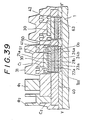
- Fig. 39 is a sectional view of this embodiment.
- the light-emitting elements are formed as follows. An n-type GaAs layer 24b, an n-type AlGaAs layer 24a, a p-type GaAs layer 23a, an n-type GaAs layer 22a, a p-type AlGaAs layer 21b, and a p-type GaAs layer 21a are sequentially formed on an n-type GaAs substrate 1.
- Isolation grooves 50 for isolating the resultant structure into individual light-emitting elements are formed by photolithography or the like and etching. An isolation groove 51 is formed to isolate the light-emitting element T (0) and the coupling diode D0.
- the embodiment F-4 adjacent elements are coupled through a pnp transistor Tr3 without using the diodes unlike in the embodiment F-1.
- the base of the transistor Tr3 is connected to the base of the transistor Tr1, and the collector of the transistor Tr3 is connected to the base of the transistor Tr2.
- the transfer operation in this case is the same as that described in the embodiment F-1. That is, the thyristor in the embodiment F-1 can be considered as the combination of the transistors Tr1 and Tr2, and the diode in the embodiment F-1 can be considered as the transistor Tr3.
- a detailed device structure in the embodiment F-4 is the same as those shown in the embodiments F-2 and F-3.
- Fig. 41 is an equivalent circuit diagram of an embodiment F-5.
- the power source V GK and the load resistors R L are omitted from the equivalent circuit shown in the embodiment F-1.
- the equivalent circuit of the embodiment F-1 utilizes the fact that the ON voltage of the thyristor is determined with respect to the power source voltage V GK , the gate voltage of the ON element becomes almost 0 V, and this influences the adjacent elements through the diodes.
- the power source V GK is omitted. An operation of this embodiment will be described below.
- Figs. 42 and 43 show a structure of an embodiment F-6.
- the structure shown in Figs. 42 and 43 corresponds to an actual structure of the equivalent circuit shown in the embodiment F-5.
- Fig. 42 is a plan view
- Fig. 43 is a sectional view taken along a line X-X′ in Fig. 42.
- n-type GaAs layer 24b, an n-type AlGaAs layer 24a, a p-type GaAs layer 23a, an n-type GaAs layer 22a, a p-type AlGaAs layer 21b, and a p-type GaAs layer 21a are sequentially formed on an n-type GaAs substrate 1.
- Isolation grooves 50 are then formed to isolate the light-emitting elements.
- Isolation grooves 51 are formed to isolate the light-emitting diodes and the coupling diodes. That is, the p-type GaAs layer 21a and the p-type AlGaAs layer 21b are removed. Insulating films 30 are formed, and contact holes C1 are formed therein. Thereafter, electrodes 41 and transfer clock lines ⁇ 1 and ⁇ 2 are formed. With the above-mentioned process, the structure of the embodiment F-6 is completed.
- the characteristic feature of the structure of the embodiment F-6 is that two-phase wiring layers are not used unlike in the embodiment F-3. As can be seen from Fig. 42, wiring patterns can be formed without overlapping, and one wiring layer need only be formed. Since a resistor can be omitted, a manufacturing process can be simplified, and thus, manufacturing cost can be further decreased.
- Fig. 44 is an equivalent circuit diagram of an embodiment F-7.
- the embodiment F-7 corresponds to one rewriting the embodiment F-5 as an equivalent circuit using transistors.
- the structure of the embodiment F-7 is substantially the same as that of the embodiment F-4, except that the load resistor in the embodiment F-4 is omitted, and its operation is the same as that in the embodiment F-5.
- the actual structure of the embodiment F-7 is the same as that in the embodiment F-6.
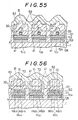
- a drive method of the optical scanning composite element will be described below. Under the connection relationship shown in Fig. 53, clock pulses are sequentially applied to the laser thyristors T (-1) , T (0) and T (1) lthrough the lines ⁇ 2, ⁇ 3 and ⁇ 1 at timings shown in Fig. 58 so as to be turned on. A laser drive current is supplied from the line ⁇ I to turn on and scan each laser.
- the above embodiments provide a self-scanning light-emitting element array which can obtain light-point scanning performance sufficiently finer than an array pitch of light-emitting elements.
Landscapes
- Physics & Mathematics (AREA)
- Optics & Photonics (AREA)
- General Physics & Mathematics (AREA)
- Engineering & Computer Science (AREA)
- General Engineering & Computer Science (AREA)
- Electromagnetism (AREA)
- Condensed Matter Physics & Semiconductors (AREA)
- Theoretical Computer Science (AREA)
- Health & Medical Sciences (AREA)
- General Health & Medical Sciences (AREA)
- Toxicology (AREA)
- Led Devices (AREA)
- Printers Or Recording Devices Using Electromagnetic And Radiation Means (AREA)
- Control Of El Displays (AREA)
- Dot-Matrix Printers And Others (AREA)
Abstract
Description
- The present invention relates to a self-scanning type light-emitting element array in which light-emitting elements are integrated on a single substrate and a method of driving the same.
- As typical light-emitting elements, an LED (light-emitting diode) and an LD (laser diode) are known.
- In the LED, a pn or pin junction of a compound semiconductor (GaAs, GaP, GaAlAs or the like) is formed, and a forward bias voltage is applied to the junction so as to inject carriers in the junction. The LED utilizes a light-emission phenomenon occurred by carrier recombination.
- In the LD, a waveguide is arranged in the LED. When a current exceeding a given threshold value is supplied, injected electron-hole pairs are increased, and a population inversion state is established. Light generated by parallel reflection mirrors utilizing a cleavage surface is fed back to an active layer, thus causing laser oscillation. Then, a laser beam is emitted from an end face of the waveguide.
- Negative resistance elements (light-emitting thyristor, laser thyristor and the like) are known as a light-emitting element having the same light-emission mechanism as those of the LED and LD. In the light-emitting thyristor, a pnpn structure is formed by a compound semiconductor described above, and a thyristor using silicon is put into practical applications.
- Figs. 22 and 23 show the basic structure and current-voltage characteristics of the negative resistance element having the light-emission function (called a light-emitting thyristor herein). The structure shown in Fig. 22 is the same as that of a thyristor in which a pnpn structure is formed on an n-type GaAs substrate. Fig. 23 also represents the same S-shaped negative resistance characteristics as those of the thyristor. Not only a two-terminal thyristor shown in Fig. 22 but also a three-terminal thyristor shown in Fig. 24 are also known. The gate of the three-terminal thyristor has a function of controlling an ON voltage. The ON voltage is converted to a voltage as a sum of a gate voltage and a diffusion potential. After the thyristor is turned on, the gate electrode voltage substantially coincides with the cathode voltage. If the cathode electrode is grounded, the gate electrode voltage becomes zero volt. As is well known, a threshold voltage of the light-emitting thyristor is decreased when light is externally incident thereon.
- A waveguide can be formed in the light-emitting thyristor to form a laser thyristor by quite the same principle as the LD (Tashiro el al., Lecture to the Japan Society of Applied Physics, Autumn 1987, No.18p-ZG-10).
- The light-emitting element described above, in particular, the LED is commercially available in such a manner that a large number of elements are formed on a compound semiconductor substrate and are cut into pieces and are packaged one by one. An LED for a contact image sensor and a light source for a printer is commercially available as an LED array in which a plurality of LEDS are arrayed on a single chip.
- A contact image sensor, an LED printer, and the like require a scanning function of light-emitting points by these light-emitting elements in order to designate read or write points.
- However, in order to perform optical scanning using the above-mentioned conventional light-emitting elements, each LED formed in the LED array must be connected to a drive IC by wire bonding or the like, and must be driven by the IC. For this reason, if a large number of LEDS are arranged, the wire bonding must be performed for portions corresponding in number to the LEDS, and a large number of drive ICs are required, resulting in high cost. A space for arranging drive ICs must be assured, and it is difficult to achieve a compact array. A pitch between adjacent LEDS is determined depending on the wire bonding technique, and it is difficult to decrease the pitch.
- According to a first aspect of the present invention, a self-scanning light-emitting element array comprises an array of light-emitting elements, turn-on threshold levels of which are able to be controlled; coupling means for coupling the elements in an array direction so that an ON light-emitting element has an influence to change the threshold level of a light-emitting element which is to be turned on next; and drive means, connected to said light-emitting elements to supply parallel drive pulses thereto, for transferring a turn-on in the array direction at an interval of drive pulses while propagating a change in threshold level in the array direction.
- According to a second aspect of the present invention, a method of driving a self-scanning light-emitting element array comprises chain-coupling a plurality of light-emitting elements so that a light-emitting element which is turned on influences an adjacent light-emitting element to be turned on next to change a threshold level; performing polyphase-drive so that the light-emitting element which is turned on and the adjacent light-emitting element to be turned on next are driven by drive pulses of different phases; controlling a valid direction and a valid range of the influence so that the influence of changing the threshold level is validated in a next one phase; and sequentially transferring a turn-on operation in one direction of the element array in a switching period of phases.
- According to a third aspect of the present invention, a self-scanning light emitting element comprises an array of light-emitting elements, turn-on threshold levels of which are able to be controlled by external light; transparent coupling portions, arranged between adjacent light-emmiting elements, for causing part of light emmited from a light-emitting element which is turned on to be incident on a light emitting element adjacent to said ON light-emitting element so as to change a threshold level of the adjacent light-emitting element to be turned on next; and drive means, connected to said light-emitting elements to supply parallel drive pulses thereto, for transferring a turn-on operation in the array direction at interval of drive pulses while propagating a change in threshold level in the array direction.
- According to a fourth aspect of the present invention a self-scanning light-emitting element array comprises an array of light-emitting elements, turn-on threshold levels of which are able to be electrically controlled; a resistor network for coupling control electrodes for controlling threshold levels of said light-emitting elements in an element array direction, so that a light-emitting element which is turned on changes the threshold level of an adjacent light-emitting element to be turned on next; and drive means, connected to said light-emitting elements to supply parallel drive pulses thereto, for transferring turn-on operation in the array direction at an interval of drive pulses while propagating a change in threshold level in the array direction.
- According to a fifth aspect of the present invention, a self-scanning light-emitting element array comprises an array of light-emitting elements, turn-on threshold levels of which are able to be electrically controlled, said array being divided into blocks each consisting of a plurality of light-emitting elements; coupling means for directly coupling control electrodes for controlling threshold levels of said light-emitting elements between adjacent blocks so that a block which is turned on changes the threshold level of an adjacent block to be turned on next, said control electrodes of the light-emitting elements in one block being not directly coupled so that a change in threshold level caused by the direct coupling is not transferred to a next to the next block; and drive means for supplying parallel drive pulses of a plurality of phases to said blocks which are assigned to the respective phases, and transferring a turn-on operation in the array direction at an interval drive pulses while propagating a change in threshold level in the array direction.
- According to a sixth aspect of the present invention, a self-scanning light-emitting element array comprises an array of light-emitting elements, turn-on threshold levels of which are able to be electrically controlled; a coupling element, having electrical directivity and interconnecting in an element array direction control electrodes for controlling threshold levels of said light-emitting elements, so that a light-emitting element which is turned on changes the threshold level of an adjacent light-emitting element to be turned on next; and drive means, connected to said light-emitting elements to supply parallel drive pulses thereto, for transferring a turn-on operation in the array direction at an interval of drive pulses while propagating a change in threshold level in one array direction.
- According to a seventh aspect of the present invention, a self-scanning light-emitting element array comprises an array of light-emitting elements, turn-on threshold levels of which are able to be electrically controlled; coupling means consisting of transistors each of which is current-mirror connected to one transistor element constituting each of said light-emitting elements, an output electrode, of the current-mirror transistor being connected to a control electrode for controlling a threshold level of an adjacent light-emitting element, so that a light-emitting element which is turned on changes the threshold level of an adjacent light-emitting element to be turned on next; and drive means, connected to said light-emitting elements to supply parallel drive pulses thereto, for transferring a turn-on operation inthe array direction at an interval of drive pulses while shifting a change in threshold level in the array direction.
- The invention will now be described by way of non-limiting embodiments with reference to the accompanying drawings, in which:-
- Fig. 1 is a schematic circuit diagram of a light-emitting element array using light in an embodiment A-1;
- Fig. 2 is a schematic sectional view of a light-emitting element array using light in an embodiment A-2;
- Fig. 3 is a schematic plan view of a light-emitting element array using light in an embodiment A-3;
- Figs. 4 and 5 are schematic sectional views of the light-emitting element array using light in the embodiment A-3;
- Fig. 6 is a schematic sectional view of a light-emitting element array using light in an embodiment A-4;
- Fig. 7 is a schematic plan view of a light-emitting element array using light in an embodiment A-5;
- Fig. 8 is a schematic sectional view of the light-emitting element array using light in the embodiment A-5;
- Fig. 9 is a schematic circuit diagram of a light-emitting element array using a potential in an embodiment B-1;
- Fig. 10 is a schematic sectional view of a light-emitting element array using a potential in an embodiment B-2;
- Fig. 11 is a schematic plan view of a light-emitting element array using a potential in an embodiment B-3;
- Figs. 12 and 13 are schematic sectional views of the light-emitting element array using a potential in the embodiment B-3;
- Fig. 14 is a schematic plan view of a light-emitting element array using a potential in an embodiment B-4;
- Fig. 15 is a schematic sectional view of the light-emitting element array using a potential in the embodiment B-4;
- Fig. 16 is a schematic circuit diagram showing a method of driving a light-emitting element array in an embodiment C and a timing chart showing pulse waveforms;
- Fig. 17 is a schematic sectional view of a proximity image sensor in an
application 1; - Fig. 18 is a schematic sectional view of an optical printer in an
application 2; - Fig. 19 is a schematic sectional view of an optical printer head in the
application 2; - Fig. 20 is a schematic plan view of an optical display in the
application 2; - Fig. 21 is a schematic sectional view showing a structure of a light-emitting thyristor of a double-hetero structure;
- Fig. 22 is a schematic sectional view showing a structure of a light-emitting thyristor;
- Fig. 23 is a graph showing current-voltage characteristics of the light-emitting thyristor;
- Fig. 24 is a schematic sectional view showing a structure of a three-terminal thyristor;
- Fig. 25 is an equivalent circuit diagram of a light-emitting element array in an embodiment D-1;
- Fig. 26 is a graph showing characteristics of the light-emitting thyristor;
- Fig. 27 is a sectional view of an embodiment D-2;
- Fig. 28 is a plan view of the embodiment D-2;
- Fig. 29 is a plan view of an embodiment D-3;
- Fig. 30 is a sectional view of an embodiment D-3;
- Fig. 31 is a plan view of an embodiment D-4;
- Fig. 32 is a sectional view of an embodiment D-4;
- Fig. 33 is an equivalent circuit diagram of a light-emitting element array in an embodiment E-1;
- Fig. 34 is a circuit diagram showing a pn image of the equivalent circuit diagram of the embodiment E-1;
- Fig. 35 is a sectional view of an embodiment E-2;
- Fig. 36 is an equivalent circuit diagram of a light-emitting element array in an embodiment F-1;
- Fig. 37 is a schematic view showing a structure of a light-emitting element array in an embodiment F-2;
- Figs. 38 and 39 are respectively a plan view and a sectional view of a light-emitting element array in an embodiment F-3;
- Fig. 40 is an equivalent circuit diagram of a light-emitting element array in an embodiment F-4;
- Fig. 41 is an equivalent circuit diagram of a light-emitting element array in an embodiment F-5;
- Figs. 42 and 43 are respectively a plan view and a sectional view of a light-emitting element array in an embodiment F-6;
- Fig. 44 is an equivalent circuit diagram of a light-emitting element array in an embodiment F-7;
- Figs. 45 and 46 are respectively a plan view and a sectional view of a light-emitting element array in an embodiment F-8;
- Fig. 47 is an equivalent circuit diagram showing an embodiment G-1;
- Fig. 48 is a sectional view showing an embodiment G-2;
- Fig. 49 is a plan view showing an embodiment G-3;
- Figs. 50 and 51 are sectional views showing the embodiment G-3;
- Fig. 52 is a schematic view showing a basic structure of embodiments H;
- Fig. 53 is an equivalent circuit diagram of an embodiment H-1;
- Fig. 54 is a partial plan view of the embodiment H-1;
- Fig. 55 is a sectional view of a laser thyristor portion of the embodiment H-1;
- Fig. 56 is a sectional view of a light deflector portion of the embodiment H-1;
- Fig. 57 is a perspective view of the laser thyristor portion and the light deflector portion;
- Fig. 58 is a drive timing chart of the embodiment H-1;
- Fig. 59 is an equivalent circuit diagram of an embodiment H-2;
- Fig. 60 is a perspective view showing a structure of a light deflector used in the embodiment H-2;
- Fig. 61 is a view showing the principle of an optical scanning system by deflection; and
- Fig. 62 is a view showing the principle of an optical scanning system using an array.
- Embodiments A to be described hereinafter utilize light as an interaction medium between the elements.
- Fig. 1 is an equivalent circuit diagram of the principle of an embodiment A-1. This diagram illustrates a case wherein a most typical three-terminal light-emitting thyristor is used as an example of a light-emitting element whose light-emission threshold voltage and current can be externally controlled.
- Light-emitting thyristors T(-2) to T(+2) are arrayed in a line. Each of three transfer clock lines (φ₁ , φ₂ and φ₃) is connected to the corresponding anode electrodes of every three light-emitting elements. A light-emitting thyristor has characteristics that its turn-on voltage is decreased when it senses light. When light-emitting thyristors are arranged so that light emitted from an ON light-emitting element is incident on another interacting light-emitting element, the turn-on voltage of an element near the ON element or an element which is arranged to sufficiently receive light from the ON element is decreased.
- The operation of the equivalent circuit diagram of Fig. 1 will be described below. Assume that a high-level pulse voltage is applied to the transfer clock line φ₃, and a light-emitting thyristor T(0) is kept on. Light LI emitted from the light-emitting thyristor T(0) is incident on light-emitting thyristors T(-1) and T(+1), thus decreasing their ON voltages. Since the light-emitting thyristors T(-2) and T(+2) are located farther than the light-emitting thyristors T(-1) and T(+1), incident light is weak, and their ON voltages are not so decreased. In this state, a high-level pulse voltage is applied to the next clock line φ₁. Since the ON voltage of the light-emitting thyristor T(+1) is decreased by the influence of light as compared to that of the light-emitting thyristor T(-2), if the high-level voltage of the transfer clock is set to be a value between the ON voltages of the light-emitting thyristors T(+1) and T(-2) , only the light-emitting thyristor T(+1) is turned on, and the light-emitting thyristor T(-2) can be kept off. Thus, the light-emitting thyristors T(+1) and T(0) are simultaneously turned on. When a low-level voltage is applied to the clock line φ₃, the light-emitting thyristor T(0) is turned off and only the light-emitting thysistor T(+1) is turned on. Thus, an ON state is transferred.
- Based on the above-mentioned principle, the high-level voltages of the transfer clocks φ₁, φ₂ and φ₃ are set to slightly overlap each other, the ON states of the light-emitting elements are sequentially transferred. More specifically, a light-emission point is sequentially transferred.
- According to this embodiment, a self-scanning type light-emitting element array which cannot be achieved by the prior art can be realized.
- In the embodiment A-1, an equivalent circuit has been presented and described. In an embodiment A-2, an IC structure of the arrangement of the embodiment A-1 will be described below.
- Fig. 2 is a schematic view of the structure. A p-
type semiconductor layer 23, an n-type semiconductor layer 22, and a p-type semiconductor layer 21 are formed on a grounded n-type GaAs substrate 1. The multilayered structure is patterned into light-emitting elements T(-2) to T(+2) by photolithography and the like and etching. Eachelectrode 40 makes an ohmic contact with the corresponding p-type semiconductor layer 21, and an insulatinglayer 30 serves as a protection film for preventing short-circuiting between an element and a wiring and at the same time preventing deterioration of characteristics. The insulatinglayer 30 is formed of a material which allows light having a light-emission wavelength of a light-emitting thyristor to pass therethrough. - The p-
type semiconductor layer 21 serves as an anode of this thyristor, and the n-type GaAs substrate 1 serves as a cathode. Each of three transfer clock lines (φ₁, φ₂ and φ₃) is sequentially connected to theanode electrodes 40 of every three light-emitting elements. - It is generally known that the ON voltage of a light-emitting thyristor is changed depending on an amount of light incident on the element. Therefore, if the light-emitting thyristors are arranged so that light emitted from an ON light-emitting thyristor is incident on adjacent light-emitting thyristors, the ON voltages of the light-emitting thyristors adjacent to the ON thyristor are decreased as compared to a case wherein no light is emitted.
- In the structure illustrated in Fig. 2, the insulating
layer 30 is formed of a transparent film with respect to a light-emission wavelength. If a light-emitting thyristor T(0) is in an ON state, light L₀ is emitted upward, and light LI is well input to adjacent elements T(-1) and T(+1), thus decreasing their ON voltages. - The operation of the light-emitting element array is the same as that in the embodiment A-1.
- Based on the above-mentioned principle, the high-level voltages of the transfer clocks φ₁, φ₂ and φ₃ are set to slightly overlap each other, the ON states of the light-emitting elements are sequentially transferred. More specifically, a light-emission point is sequentially transferred. According to this embodiment, an integrated self-scanning type light-emitting element array utilizing light coupling, which cannot be achieved by the prior art, can be realized.
- In this embodiment, a practical structure of the embodiment A-2 will be described.
- Fig. 3 is a plan view of this embodiment, and Figs. 4 and 5 are sectional views taken along lines X-X′ and Y-Y′ in Fig. 3, respectively.
Isolation grooves 50 are formed between adjacent ones of light-emitting elements T(-2) to T(+1). Light barriers 61 are partially formed in theisolation grooves 50 so as not to cause light from an ON light-emitting element to become incident on elements other than two adjacent elements. - In this embodiment, projections of a
field 60 are used as thelight barriers 61. However, other materials may be used, or other shapes may be employed. A contact hole C₁ is formed in an upper electrode of each light-emitting element, and is electrically connected to anelectrode 40. A contact hole C₂ is a through hole to be connected to a corresponding one of transfer clock lines φ₁, φ₂ and φ₃. - The transfer clock line φ₁ is connected to the light-emitting elements T(-2) and T(+1), the transfer clock line φ₂ is connected to the light-emitting element T(-1), and the transfer clock line φ₃ is connected to the light-emitting element T(0).
- Fig. 4 is a sectional view taken along a line X-X′ in Fig. 3. This line is parallel to the array direction of the light-emitting element array, and Fig. 4 reveals a state of the light-emitting elements arrayed in a line. An insulating
film 30 for preventing short-circuiting between each light-emitting element and theelectrode 40 and an insulatingfilm 31 as an insulating interlayer for preventing short-circuiting between theelectrode 40 and the transfer clock line are formed to surround theisolation groove 50 so as to be adjacent to theisolation groove 50 of each light-emitting element. These insulatingfilms film 31 which properly absorbs light and a transparent insulating film may be stacked to have an appropriate film thickness. With this structure, light coupling between adjacent elements can be established, and a transfer operation (light scanning operation) can be performed. The film structure of the light-emitting element is the same as that shown in Fig. 21 (to be described later). - Fig. 5 is a sectional view taken along a line Y-Y′ in Fig. 3. This line is perpendicular to the array direction of the light-emitting element array, and Fig. 5 reveals a connection state of wirings and electrodes. The contact hole C₁ led to the upper electrode of each light-emitting element is formed in the insulating
film 30, and is externally led to an external portion through theelectrode 40. Theelectrode 40 is connected to the transfer clock line φ₃ via the through hole C₂. - A manufacturing process for realizing this embodiment is as follows.
- An n-
type GaAs layer 24b, an n-type AlGaAs layer 24a, a p-type GaAs layer 23a, an n-type GaAs layer 22a, a p-type AlGaAs layer 21b, and a p-type GaAs layer are sequentially formed and stacked on an n⁺-type GaAs substrate 2 by epitaxial growth. Theisolation grooves 50 are formed using a photoetching technique. Thereafter, the insulatingfilm 30 is formed, and the contact holes C₁ are formed therein using the photoetching technique. A metal electrode layer is then formed by a deposition or sputtering method, and theelectrodes 40 are formed using the photoetching technique. The insulatingfilm 31 is formed, and the through holes C₂ are formed using the photoetching technique. A metal wiring layer is formed by the deposition or sputtering method, and the transfer clock lines (φ₁, φ₂ and φ₃) are formed by the photoetching technique. With the above-mentioned process, the structure of this embodiment is completed. - Although not described in this embodiment, a transparent protection film may be formed on the transfer clock lines. If it is not preferable that the thickness of the insulating film is too large to degrade a transmittance of light and to decrease an amount of externally output light, part or all of the upper insulating film of the light-emitting element may be removed by, e.g., photoetching.
- According to this embodiment, an integrated self-scanning light-emitting element array can be manufactured.
- In the embodiments A-2 and A-3, the light-emitting thyristor is adopted as the light-emitting element. However, the present invention is not limited to this, various other light-emitting elements may be adopted.
- In this embodiment, for example, a case will be described below wherein a laser thyristor is used.
- Fig. 6 is a sectional view when a laser thyristor is used as a light-emitting element. Light-emitting elements (laser thyristors) T(-1) to T(+1) are formed to have the following structure. An n-
type AlGaAs layer 125, a p-type AlGaAs layer 124, an i-type (non-doped)GaAs layer 123, an n-type AlGaAs layer 122, and a p-type AlGaAs layer 121 are sequentially stacked on an n-type GaAs substrate 1. The p-type AlGaAs layer 121 and the n-type AlGaAs layer 122 are patterned as shown in Fig. 6. The shape illustrated in Fig. 6 is the same as that of a conventional stripe type laser diode. The entire width of the p-type AlGaAs layer 121 and the partial width of the n-type AlGaAs layer 122 are 10 µm or less. Other portions are the same as those in Figs. 2 to 5 described above. - In an operation of the laser thyristor, the same operation as in a conventional light-emitting thyristor is performed until a current component supplied to the thyristor reaches a laser oscillation current, and light emitted by a current component below the laser oscillation current is isotropically output. A laser beam is output in a direction perpendicular to the sheet surface of Fig. 6. Therefore, the laser beam does not contribute to light coupling between adjacent elements, and light emitted by a current component below the laser oscillation current contributes to light coupling. Other mechanisms of the transfer operation are the same as those in the embodiment A-2.
- Figs. 7 and 8 show an embodiment A-5 presenting a practical structure of the embodiment A-4. Fig. 7 is a plan view, and Fig. 8 is a sectional view taken along a line X-X′ in Fig. 7. A manufacturing method of the structure shown in Fig. 7 will be briefly described below. An n-
type AlGaAs layer 125, a p-type AlGaAs layer 124, an i-type (non-doped)GaAs layer 123, an n-type AlGaAs layer 122, a p-type AlGaAs layer 121, and anupper electrode layer 20 are sequentially stacked on an n-type GaAs substrate 1 (a p-type GaAs layer for improving an ohmic contact may be formed between the p-type AlGaAs layer 121 and the upper electrode layer 20). Theupper electrode layer 20 is patterned into a rectangular shape having the same width as that of the n-type AlGaAs layer 125 in Fig. 8. Using theelectrode pattern 20 as a mask, the p-type AlGaAs layer 121 to the n-type AlGaAs layer 125 are etched. In this case,element isolation grooves 50 are formed. Theupper electrode pattern 20 is further etched into a stripe shape having a width of 10 µm or less. Using thenew electrode pattern 20 as a mask, the p-type AlGaAs layer 121 and the n-type AlGaAs layer 122 are etched. The n-type AlGaAs layer 122 is not entirely removed but is partially left. An insulatingfilm 30 is formed on the resultant structure, and through holes C2 are formed by photoetching. Thereafter, a metal wiring layer for transfer clock lines are formed by deposition or sputtering, and the transfer clock lines (φ₁, φ₂ and φ₃) are formed by photoetching. Finally, the end face of a laser beam output side is formed by cleavage or the like to have good parallelness, thus completing the structure of this embodiment. - In a conventional integrated light-emitting element array, pn junction diodes are independently formed on a single substrate, are externally led one by one using a wire bonding technique, and are operated by applying a voltage by drive ICs. Thus, assembly such as a wiring bonding process is cumbersome, resulting in high cost. In contrast to this, in a light-emitting element array of this embodiment, three transfer clock terminals need only be externally lead, and assembly is considerably simplified. At the same time, a space for drive ICs can be omitted, and a compact self-scanning light-emitting element array as a whole can be produced. In a conventional array, an alignment pitch of light-emitting elements is predetermined depending on the bonding technique. However, the above-mentioned embodiments A-1 to A5 are free from such a restriction, and a light-emitting element array having a smaller pitch can be manufactured. Thus, an application to a device having a very high resolution can be achieved.
- In the embodiments A-1 to A-5, the transfer clock pulses are assumed to have three phases, i.e., φ₁, φ₂ and φ₃. The number of phases may be increased to four or five so as to attain a more stable transfer operation. A larger amount of light emitted by a light-emitting thyristor T(0) is caused to incident on a light-emitting thyristor T(+1) than to a light-emitting thyristor T(-1), so that the elements can be driven by two-phase clocks. For example, light-emitting thyristors are arranged in an asymmetrical planar pattern, so that a larger amount of light is emitted to the right in the arrangement.
- In the above embodiment, the simplest structure of the light-emitting thyristor has been described. The scope of the present invention includes adaption of a more complex structure and a multilayer structure in order to increase light-emission efficiency. This also applies to many embodiments to be described later. For example, a double-hetero structure may be employed. Fig. 21 shows an example of the double-hetero structure (Tashiro et al., Lecture to the Japan Society of Applied Physics, Spring, 1987, No. 28p-ZE-8). In this structure, an n-
type GaAs layer 24b having a thickness of 0.5 µm) is formed on an n-type GaAs substrate 1. An n-type AlGaAs layer 24a (1 µm) having a wide band gap, a p-type GaAs layer 23a (5 nm), an n-type GaAs layer 22a (1 µm), a p-type AlGaAs layer 21b (1 µm) having a wide band gap, and a p-type GaAs layer 21a (0.15 µm) for making an ohmic contact with a lead electrode are sequentially stacked on theGaAs layer 24b. A light-emission layer is the n-type GaAs layer 22a (1 µm) sandwiched between thelayers GaAs layer 22a having a narrow band gap, and are recombined in this region to emit light. - The light-emitting element need not always be a light-emitting thyristor, and is not particularly limited if its turn-on voltage is changed by light. For example, the above-mentioned laser thyristor may be employed.
- In the above embodiment, a pnpn thyristor structure has been exemplified. A structure whose threshold voltage is decreased by light and which is caused to perform a transfer operation by utilizing this function is not limited to the pnpn structure or any other specific structure if it can achieve the above function. For example, if a multilayered structure of six layers or more is employed in place of a pnpn four-layered structure, the same effect can be expected, and the same self-scanning function can be achieved. Furthermore, the same effect may be obtained if another type of thyristor, e.g., a static induction (SI) thyristor or a field control thyristor (FCT), is used. The SI thyristor or the FCT has a structure wherein a central p-type semiconductor layer serving as a current block is replaced with a depletion layer (S.M. Sze, Physics of Semiconductor Devices, 2nd Edition, pp. 238-240).
- In the embodiments A-1 to A-5, the light-emitting elements are arrayed in a line, but need not be arranged along a straight line. For example, the elements may be arranged in a zigzag manner depending on applications. The elements may be arranged in two lines from the halfway.
- According to the present invention, the light-emitting elements may be constituted by individual parts, or may be integrated by any means.
- Embodiments B described herein utilize a potential as an interaction medium.
- The embodiments A-1 to A-5 shown in Figs. 1 to 8 utilize coupling by means of light. This embodiment utilizes coupling by means of a potential.
- Fig. 9 is an equivalent circuit diagram of an embodiment B-1 of the present invention. The characteristic feature of this embodiment is that a resistor network is added to the arrangement in the embodiment A-1, i.e., Fig. 1.
- As light-emitting elements, light-emitting thyristors T(-2) to T(+2) are used. The light-emitting thyristors T(-2) to T(+2) have gate electrodes G₋₂ to G₊₂, respectively. A power source voltage VGK is applied to each gate electrode through a corresponding load resistor RL. The gate electrodes G₋₂ to G₊₂ are electrically connected to each other through resistors RI to achieve an interaction. Each of three transfer clock lines φ₁, φ₂ and φ₃ is sequentially connected to the anode electrodes of every three light-emitting elements.
- An operation will be described below. Assume that the transfer clock φ₃ goes to high level, and the light-emitting element T(0) is turned on. In this case, a potential at the gate electrode G₀ is reduced to about 0 V due to the characteristics of the three-terminal thyristor (about 1 V for a silicon thyristor). Assuming that the power source voltage VGK is 5 V, the gate voltage of each light-emitting thyristor is determined by the network of the load resistors RL and the resistors RI. A gate voltage of an element nearest the light-emitting element T(0) is decreased by the largest amount, and a gate voltage is increased as an element is separated from T(0). This can be expressed as follows:
VG0 < VG-1 = VG-1< VG2 = VG-2 ...(1) - A difference between these voltages can be set by appropriately selecting the values of the load resistors RL and resistors RI.
- As is well known, a turn-on voltage VON at the anode side of the three-terminal thyristor is higher than a gate voltage VG by a diffusion voltage Vdf.
VON ≒ VG + Vdf (2)
Therefore, if a voltage applied to the anode is set to be higher than the turn-on voltage VON, the corresponding light-emitting thyristor is turned on. - In a state wherein the thyristor T(0) is kept on, a high-level voltage VH is applied to the next transfer clock pulse φ₁. The clock pulse φ₁ is simultaneously applied to the light-emitting elements T(+1) and T(-2). If the value of the high-level voltage VH is set to fall within the following range, only the light-emitting element T(+1) can be turned on.
VG-2 + Vdf > VH > VG+1 + Vdf (3)
Thus, both the light-emitting elements T(0) and T(+1) are kept on. When the high-level voltage VH of the clock pulse φ₃ is disabled, the light-emitting element T(0) is turned off, and an ON state can be transferred. - In this manner, the gate electrodes of the light-emitting thyristors are connected through the resistor network, thus providing a transfer function to the light-emitting elements.
- With the above-mentioned principle, the high-level voltages VH of the transfer clock lines φ₁, φ₂ and φ₃ are set to sequentially slightly overlap each other, so that the ON states of the light-emitting elements are sequentially transferred. More specifically, a light-emission point is sequentially transferred. According to this embodiment, a self-scanning type light-emitting element array which cannot be achieved by a prior art technique can be realized.
- In the embodiment B-1, the equivalent circuit has been exemplified. In the embodiment B-2, an IC structure of the arrangement of the embodiment B-1 will be described.
- Fig. 10 shows a structure of this embodiment. An n-
type semiconductor layer 24, a p-type semiconductor layer 23, an n-type semiconductor layer 22, and a p-type semiconductor layer 21 are sequentially formed on a grounded n-type GaAs substrate 1.Isolation grooves 50 for isolating the multilayered structure into light-emitting elements T(-1) to T(+1) are formed by, e.g., photolithography or the like and etching. Eachanode electrode 40 has an ohmic contact with the p-type semiconductor layer 21, and eachgate electrode 41 has an ohmic contact with the n-type semiconductor layer 22. An insulatinglayer 30 prevents short-circuiting between the elements and wiring layers, and also serves as a protection film for preventing deterioration of characteristics. The insulatinglayer 30 is preferably formed of a material which allows light having a light-emission wavelength of a light-emitting thyristor to pass therethrough well. The n-type GaAs substrate 1 serves as a cathode of each thyristor. Three transfer clock lines φ₁, φ₂ and φ₃ are connected to the anode electrodes of the light-emitting elements. The gate electrodes are connected to a resistor network through load resistors RL and interaction resistors RI. - When light coupling described in the embodiment A occurs, it affects the transfer operation of this embodiment. The
gate electrodes 41 are partially formed in theisolation grooves 50 between the light-emitting elements to provide a structure for preventing light coupling. - The structure of this embodiment is the same as the equivalent circuit shown in the embodiment B-1 (Fig. 9), and performs the same operation. Therefore, if the high-level voltages of the transfer clock lines φ₁, φ₂ and φ₃ are set to sequentially slightly overlap each other, an ON state of light-emitting thyristors is sequentially transferred. More specifically, a light-emission point is sequentially transferred.
- Figs. 11, 12, and 13 show an embodiment B-3. This embodiment presents an actual structure of the embodiment B-2. Fig. 11 is a plan view of this embodiment, and Figs. 12 and 13 are sectional views taken along lines X-X′ and Y-Y′ in Fig. 11, respectively.
- Light-emitting elements T(-1) to T(+1), isolation grooves of the light-emitting elements, and a
field layer 60, and the like are the same as those in the embodiment A-3. A two-dimensional resistor 63 forms a resistor network connecting the gate electrodes. Light emitted from the light-emitting elements is prevented from being input to theresistor 63 by light absorbing blocks 62. In this embodiment, a portion of thefield layer 60 is used as an optical barrier. However, other materials may be used or another shape may be employed. An upper electrode of each light-emitting element is led via a lead contact hole C₁ using anelectrode layer 40. A clock line φ₁ is connected to the light-emitting elements T(-2) and T(+1), a clock line φ₂ is connected to the light-emitting element T(-1), and a clock line φ₃ is connected to the light-emitting element T(0). Theresistor 63 is externally led using each contact hole C₃, and is connected to agate electrode 41 of each element. The other end portion of theresistor 63 is connected to avoltage source line 42 for supply a voltage VGK through the contact hole C₃. - Fig. 12 is a sectional view taken along a line X-X′ in Fig. 11. This line extends along an array direction of the light-emitting element array, and Fig. 12 reveals an arrayed state of the light-emitting elements. Short-circuiting preventing insulating
films 30 preventing short-circuiting between the light-emitting elements and theelectrodes films 31 as insulating interlayers for preventing short-circuiting between theelectrodes 50 and the transfer clock lines, and the like which are formed in theisolation grooves 50 of the light-emitting elements are the same as those in the embodiment A-3. These insulatingfilms gate electrodes 41 can be advantageously formed in theisolation grooves 50 to shield light. - Fig. 13 is a sectional view taken along a line Y-Y′ in Fig. 11. This line extends to be perpendicular to the array direction of the light-emitting element array, and Fig. 13 reveals a connection state of the wirings and electrodes. Lead contact holes C₁ of the light-emitting elements for the upper electrodes are formed in t!ie insulating
films 30, and are externally led using the electrode layers 40. Eachelectrode layer 40 is connected to the transfer clock line φ₃ via a through hole C₂ on thefield layer 60. As theresistor 63 for the resistor network, an n-type GaAs layer 22a of an n-type semiconductorlayer is used in this embodiment. This layer may be another layer, and another type of film may be formed by, e.g., sputtering without using a semiconductor layer. - Each
gate electrode 41 is formed to extend into theisolation groove 50 so that light emitted by the light-emitting element does not influence the resistance of theresistor 63. - The following manufacturing process for realizing this embodiment can be employed.
- An n-
type GaAs layer 24b, an n-type AlGaAs layer 24a, a p-type GaAs layer 23a, an n-type GaAs layer 22a, a p-type AlGaAs layer 21b, and a p-type GaAs layer 21a are sequentially grown on an n⁺-type GaAs substrate 21 by an epitaxial growth method.Isolation grooves 50 are then formed by photoetching. Portions of the light-emitting elements and p-type GaAs layer 21a and the p-type AlGaAs layer 21b in the resistor portion are removed by photoetching using another mask. Thereafter, an insulatingfilm 30 is formed, and contact holes C₁ are formed by photoetching. A metal electrode layer is formed by deposition or sputtering, andelectrodes film 31 is formed, and through holes C₂ are formed by photoetching. A metal wiring layer is then formed by deposition or sputtering, and transfer clock lines φ₁, φ₂ and φ₃ are formed by photoetching. With the above process, the structure of this embodiment is completed. - Although not particularly described in this embodiment, a transparent protection film may be formed on the transfer clock lines. If it is not preferable that the thickness of the insulating film is too large to degrade the transmittance of light and to decrease an amount of externally output light, part or all of the upper insulating film of the light-emitting element may be removed by, e.g., photoetching.
- According to this embodiment, an integrated self-scanning light-emitting element array can be manufactured.
- In the embodiments B-2 and B-3, the light-emitting thyristor is adopted as the light-emitting element. In this embodiment, a case will be described below wherein a laser thyristor is used.
- Fig. 14 shows an embodiment B-4. Fig. 14 is a plan view, and Fig. 15 is a sectional view taken along a line X-X′ in Fig. 14.
- Reference symbols such as T(-1) to T(+1) of the light-emitting elements (laser thyristors), and the like are the same as those in the above embodiment.
- A manufacturing method of Fig. 14 will be described below. An n-
type AlGaAs layer 125, a p-type AlGaAs layer 124, an i-type (non-doped)GaAs layer 123, an n-type AlGaAs layer 122, a p-type AlGaAs layer 121, and anupper electrode layer 20 are sequentially stacked on an n-type GaAs substrate 1 (a p-type GaAs layer for improving an ohmic contact may be formed between the p-type AlGaAs layer 121 and the upper electrode layer 20). Theupper electrode layer 20 is patterned into a rectangular shape having the same width as that of the n-type AlGaAs layer 125 in Fig. 15. Using theelectrode pattern 20 as a mask, the p-type AlGaAs layer 121 to the n-type AlGaAs layer 125 are etched to formelement isolation grooves 50. Theupper electrode pattern 20 is further etched into a stripe shape having a width of 10 µm or less. Using thenew electrode pattern 20 as a mask, the p-type AlGaAs layer 121 and the n-type AlGaAs layer 122 are etched. The n-type AlGaAs layer 122 is not entirely removed but is partially left. Insulatingfilms insuiating films light shielding film 30b, so that two functions, i.e., insulating and light shielding functions are provided. When an SiO₂ film is used as an insulating film, it allows a light component having a light-emission wavelength of 870 nm of GaAs to pass therethrough, it may induce light coupling. Thus, thelight shielding film 30b formed of a light absorption material, e.g., amorphous silicon, must be formed between the insulating films. Of course, if a material having both the two insulating and light shielding functions is used, one layer need only be formed. Contact holes C₁ are formed by photoetching, and aresistor 63 is formed thereon and is photoetched. An insulatingfilm 31 as an insulating interlayer is formed on the resultant structure, and through holes C₂ are formed by photoetching. In this case, the through holes on theresistor 63 can be formed by only the insulatingfilm 31. However, the through holes on theupper electrode 20 must be carefully formed since the insulatingfilms - The light-emitting element arrays in the embodiments B-1 to B-4 have a self-scanning function as in the embodiments A, which cannot be achieved by a conventional light-emitting element array and can provide effects of efficient assembly, compactness, a decrease in pitch, and the like.
- In the embodiments B-1 to B-4, the transfer clock pulses are assumed to have three phases, i.e., φ₁, φ₂ and φ₃. The number of phases may be increased to four or five so as to attain a more stable transfer operation.
- In the above embodiments, the light-emitting elements are arrayed in a line. However, the elements need not be arranged in a line but may be arranged in a zigzag manner depending on applications. The elements may be arranged in two lines from the halfway.
- The light-emitting element need not be a light-emitting thyristor. The present invention is not particularly limited to any element as long as a turn-on voltage of a light-emitting element is changed by an external potential. The light-emitting element may be a laser thyristor as described above.
- According to the present invention, the light-emitting elements may be constituted by individual parts, or may be integrated by any means.
- The structure of the light-emitting thyristor is not particularly limited. For example, a more complex structure and a multilayer structure may be adopted, and an arbitrary structure constituted by six or more layers may be adopted, as described in the embodiments A.
- In the series of embodiments A and B of the present invention, a semiconductor substrate is used as a substrate, and its potential is set at 0 V (ground potential). However, the present invention is not limited to this, and other materials may be used for the substrate. For example, an n-type GaAs layer corresponding to the n-
type GaAs substrate 1 of this embodiment is formed on a Cr-doped semiinsulating GaAs substrate, and the structure described in the above embodiments may be formed thereon. Alternatively, a semiconductor film is formed on an insulating substrate of, e.g., glass, alumina, or the like, and the structure of this embodiment may be formed using this semiconductor. - The structure of the laser is not limited to that described in the above embodiments. For example, a TJS type, a BH type, a CSP type, a VSIS type, and the like may be employed (S.M. Sze, Physics of Semiconductor Devices, 2nd Edition, pp. 724-730). As for a material, AlGaAs has been mainly described. However, other materials [e.g., AlGaInP, InGaAsP, ZnSe, GaP, and the like) may be used.
- In the embodiments A and B, an ON light-emitting element gives a primary influence to adjacent light-emitting elements, and the adjacent light-emitting elements become light-emitting elements to be driven next. However, the present invention is not limited to this. For example, an ON element may influence every other elements, so that an ON state can be transferred to every other elements.
- The above-mentioned many modifications will be applied to the following numerous embodiments.
- An embodiment C to be described below is related to a drive method of the light-emitting element arrays produced by the Embodiments A and B described above.
- Fig. 16 is a view for explaining an embodiment C-1. Fig. 16 shows an equivalent circuit diagram representing a drive principle and pulse waveforms applied to terminals.
- In this embodiment, current sources I₁, I₂ and I₃ are arranged in parallel with transfer clock pulses φ₁, φ₂ and φ₃, and a current amount IT is controlled by a light-emission signal φI.
- An operation will be described below. A light-emitting element T(0) is turned on in response to a start pulse φS. When the transfer pulses φ₁, φ₂ and φ₃ are sequentially applied, an ON state is transferred. This mechanism has already been described in the embodiments A and B.
- Assuming that a light-emitting element T(3) is caused to emit light at a higher intensity, the light-emission signal φI is synchronously set at high level when a light-emission point has reached the position of the element T(3). In synchronism with the signal φI, currents flow from the current sources I₁, I₂ and I₃. The anode of the ON element T(3) can drain the current from the current sources. Since other light-emitting elements are in an OFF state, they cannot drain the currents, and the currents flowing into these elements flow out toward a driver which generates transfer clock pulses. Therefore, the anode current of the ON light-emitting element is increased, and a light-emission intensity is also increased.
- Fig. 16 also illustrates a waveform of the light-emission intensity L. As can be apparent from this waveform, the light-emission intensity of the light-emitting element T(3) is increased as compared to other light-emission intensities obtained when no currents from the current sources flow. When this drive method is used, the light-emission intensity at an arbitrary position can be increased, and a locational optical write operation can be performed.
- When laser thyristors are used as the light-emitting elements of this embodiment, if the anode current by the transfer clock is set to be a threshold current of laser oscillation, no laser beam is emitted in a normal transfer state, and only when a light-emission signal is input, a laser beam can be emitted.
- Applications described hereinafter related to an application of the light-emitting element arrays in the embodiments A and B and the drive method described in the embodiment C.
- Fig. 17 shows the principle of a contact type image sensor as a first application of the present invention. In this application, a function of shifting a light-emission point can be realized by the present invention, and is applied to position scanning.
- In Fig. 17, a photosensor of amorphous Si is formed on a glass substrate. In a conventional sensor, the photosensor is divided into 100-µm pixels, and these pixels are scanned by read ICs to extract outputs. Illumination is uniformly made by LEDs. In a method described herein, the amorphous Si photosensor is not divided into pixels but illumination is scanned.
- In Fig. 17, an electrode A2 serving as a light shielding layer, an amorphous Si layer A3, a transparent electrode A4, and an electrode A5 are formed on a glass substrate A1. This structure utilizes a phenomenon that the resistances of the electrodes A2 and A5 are decreased upon incidence of light since the electrical conductivity of the amorphous Si layer A3 is increased by light. A transparent protection layer A6 is formed on this structure, and a document A7 is brought into contact with the layer A6. A light-emitting element array A10 of this embodiment is arranged at a side opposite to the document A7 with respect to the glass substrate A10. A scanning beam A11 from the array A10 passes through a rod lens array A9, then passes through a window A8, formed at the central portion of the photosensor, for introducing a beam, and is then focused on the document A7.
- The light-emitting element array A10 has a function of sequentially shifting a light-emission point according to the present invention. Thus, a focal point on the document is sequentially shifted accordingly. If a tone changes due to a presence of a character on the document A7, reflection beams A12 from the document are changed accordingly. Changes in beam intensity are read by the photosensor of the amorphous Si layer A3.
- When the light-emitting element array comprises laser thyristors, a light-emitting element array having a large amount of light can be obtained due to its high quantization efficiency, thus saving power consumption and allowing high-speed reading.
- In this manner, the light-emitting element array according to the present invention can be applied to reading of characters or an image of a document, or the like, and a wide application range for a facsimile system, a bar code reader, a copying machine, and the like, can be expected.
- As a second application of the present invention, an application to an optical printer will be described below. Conventionally, an application to an optical printer using a module in which a drive IC is connected to each pixel of an LED array is known. Fig. 18 shows the principle of an optical printer. A layer of a material, e.g., amorphous Si having optical conductivity (photosensitive body) is formed on the surface of a cylindrical photosensitive drum B1. The drum B1 is rotated in a direction of an arrow a at a print speed. The surface of the photosensitive body is uniformly charged by a charger B7. A light-emitting element array optical print head B8 radiates an optical dot image to be printed onto the photosensitive body so as to neutralize a charge of a portion irradiated with a light beam. A toner is attracted to the photosensitive body in accordance with a charged state on the photosensitive body by a developing unit B10. The toner image is transferred onto a paper sheet B9 fed from a cassette B11 by a transfer unit B2. The toner image on the paper sheet B9 is heated by a fixing unit B3 and is fixed thereon. The sheet B9 is then transferred to a stacker B4. The charge on the drum which completes the transfer is neutralized over the entire surface by a discharging lamp B5, and the residual toner is removed by a cleaner B6.
- The light-emitting element array according to the present invention is driven by the drive method described in the embodiment C-1, and is applied to the light-emitting element array optical print head B8. Fig. 19 shows the structure of the optical print head B8. The head B8 is constituted by a light-emitting element array B12 and a rod lens array B13, so that a focal point of the lens is formed on the photosensitive drum B1. When the drive method described in the embodiment C-1 is used, a light-emission intensity can be increased at a position where an optical write operation is to be performed, while transferring an ON state in the light-emitting element array of the present invention. Therefore, image data can be written on the photosensitive drum.
- When the light-emitting element array comprises laser thyristors, a light-emitting element array having a large amount of light can be obtained due to its high quantization efficiency, thus saving power consumption or allowing high-speed write access, i.e., printing.
- Thus, the present invention oan be applied to the optical printer.
- The light-emitting element array for the optical printer has a linear arrangement. If the arrays are two-dimensionally arranged, a display can be prepared. This structure is shown in Fig. 20. If N light-emitting element arrays B14 are arranged, an image signal can be written from φI(1) to φI(N). If an integrated light-emitting element array is used, a high-density display element can be produced. If independent light-emitting elements are combined, a large-area display can be produced.
- Embodiments D described herein can simplify a structure of the lighT-emitting element array in the embodiments B describEd above.
- Fig. 25 is an equivalent circuit diagram showing the principle of an embodiment D-1. In this embodiment, a three-terminal light-emitting thyristor is used as a light-emitting element whose light-emission threshold voltage and current can be externally controlled. Light-emitting thyristors T(-2) to T(+2) are aligned in a line. Each light-emitting thyristor is represented as a combination of transistor Tr1 and Tr2. The transistor Tr1 is a pnp transistor, and the transistor Tr2 is an npn transistor. Each connecting resistor RL between adjacent light-emitting thyristors is connected between the bases of the adjacent npn transistors Tr2. Each of three transfer clock lines φ₁, φ₂ and φ₃ is sequentially repetitively connected to the anode electrodes of every third light-emitting thyristor. A resistor Re for regulating a current of the clock line is provided to each clock line.
- An operation will be described below. Assume that a transfer clock φ₃ goes to high level, and a light-emitting thyristor T(0) is turned on. In this case, the base of the npn transistor Tr2(0) is set at a potential capable of flowing an ON current of the light-emitting thyristor T(0) This potential is transmitted to the bases of the npn transistors Tr2(-1) and Tr2(1) of the adjacent light-emitting thyristors T(-1) and T(1) through the corresponding connecting resistors RL, and their base currents flow. As long as the transfer clock lines φ₁ and φ₂ are set at low level, the light-emitting thyristors T(-1) and T(1) are kept off. If the resistance of the connecting resistor RL is low, the npn transistors Tr2(-1) and Tr2(1) have powers capable of flowing the same current as the ON current of the light-emitting thyristor T(0) However, if the resistance of the connecting resistor RL is high, the base currents of the npn transistors Tr2(-1) and Tr2(1) are regulated by the connecting resistors RL, and the current drive powers of the npn transistors Tr2(-1) and Tr2(1) are decreased. The base currents of the npn transistors Tr2(-2) and Tr2(2) located farther than the npn transistors Tr2(-1) and Tr2(1) are further decreased, and their current drive powers are decreased more.
- As is well known, when the base current amount of the npn transistor Tr2, i.e., the current drive power is increased, the ON voltage of the light-emitting thyristor is decreased. Fig. 26 illustrates this state. The anode voltage (emitter voltage of the pnp transistor Tr1) is plotted along the abscissa, and the anode current is plotted along the ordinate. In Fig. 26, an ON voltage VS is free from an external influence. An ON voltage VS(1) represents an ON voltage of the light-emitting thyristor T(1) and an ON voltage VS(-2) represents an ON voltage of the light-emitting thyristor T(-2). A minimum voltage necessary for maintaining an ON state is called a hold voltage Vh. The ON voltages of the light-emitting thyristors T(-1) and T(1) closest to the ON light-emitting thyristor T are decreased for the above-mentioned reason, and reach the ON voltage VS(1). The ON voltages of the next closest light-emitting thyristors T(-2) and T(2) become the ON voltage VS(2) since the influence of the base current is small.
- In Fig. 25, a clock pulse φ₁ next to the clock pulse φ₃ is applied to the light-emitting thyristors T(1) and T(-2). Since their ON voltages respectively become ON voltages VS(1) and VS(-2) for the above-mentioned reason, if the high-level voltage of the clock pulse is set to be a value between the ON voltages VS(1) and VS(-2), only the light-emitting thyristor T(1) can be turned on. If the clock pulses φ₁, φ₂ and φ₃ are set so that their high-level intervals appear to overlap each other, the ON light-emitting element is sequentially transferred. Thus, a light-emitting element array capable of self-scanning can be realized.
- As described above, according to the present invention, only one resistor connecting adjacent light-emitting elements is required, and the light-emitting element array can be formed by a simple manufacturing process.
- In this embodiment, three-phase transfer clock pulses are used. The light-emitting element array of this embodiment can be operated by clock pulses of four or more phases.
- In the embodiment D-1, the equivalent circuit has been described. In an embodiment D-2, an IC structure of the arrangement in the embodiment D-1 will be described. The gist of this embodiment lies in a structure wherein a connecting resistor for performing electrical connection is formed by utilizing a portion of a light-emitting element, so that a resistor element can also be formed by the same process as in the light-emitting thyristor.
- Fig. 27 is a sectional view of the structure of this embodiment. An n-
type semiconductor layer 24, a p-type semiconductor layer 23, an n-type semiconductor layer 22, and a p-type semiconductor layer 21 are formed on a grounded n-type GaAs substrate 1.Isolation grooves 50 for isolating the above structure into individual light-emitting elements T(-2) to T(2) are formed by photolithography or the like and etching. - The n-
type GaAs substrate 1 serves as the cathode of each thyristor. Each of transfer clock lines φ₁, φ₂ and φ₃ is connected to every second p-type semiconductor layer 21 serving as the anodes of the light-emitting elements. The characteristic feature of this structure is that the p-type semiconductor layer 23 constituting the thyristors is connected through the elements. The internal resistance of the p-type semiconductor layer 23 serves as the connecting resistor RL in the embodiment D-1 shown in Fig. 25. - Fig. 28 is a plan view showing the structure of this embodiment. In the light-emitting elements T(-2) to T(2) when viewed from the above in Fig. 27, inner rectangles correspond to the p-type semiconductor layers 21, and a portion therearound corresponds to the p-
type semiconductor layer 23. In this structure,notches 55 are formed in the p-type semiconductor layer 23. Thenotches 55 are used for changing the value of the connecting resistor RL described in the embodiment D-1. If alarge notch 55 is formed, the resistance of the connecting resistor RL is increased. Therefore, in this embodiment, the connecting resistor RL can be desirably changed and optimized, thus achieving a more stable transfer operation. - The structure of this embodiment is the same as that of the equivalent circuit in the embodiment D-1 (Fig. 25), and performs the same operation. Therefore, if the high-level voltages of the transfer clocks φ₁, φ₂ and φ₃ are set to sequentially slightly overlap each other, the ON states of the light-emitting thyristors are sequentially transferred. That is, a light-emission point can be sequentially shifted.
- As described above, according to this embodiment, no gate electrode is required, and one resistor for connecting adjacent light-emitting elements need only be formed. In addition, the connecting resistor RL can be formed by a semiconductor layer constituting the light-emitting elements. As can be understood from the above description, the structure of this embodiment can be formed by a simple manufacturing process.
- In this embodiments, the transfer clock pulses are assumed to have three phases, i.e., φ₁, φ₂ and φ₃. The number of phases may be increased to four or five so as to attain a more stable transfer operation.
- Figs. 29 and 30 show an embodiment D-3. This embodiment presents a practical structure of the embodiment D-2. Fig. 29 is a plan view, and Fig. 30 is a sectional view taken along a line X-X′ in Fig. 29.
- The plan view of Fig. 29 will now be explained. Transfer clock lines φ₁, φ₂ and φ₃ are connected to
underlying anode electrodes 40 via through holes C₂. Eachanode electrode 40 is connected to a p-type GaAs layer 21a as a p-type semiconductor layer of each light-emitting element. In light-emitting elements T(-2) to T(2), a p-type GaAs layer 23a as a p-type semiconductor layer is illustrated around the rectangular p-type GaAs layers 21a.Notches 55 described in the embodiment D-2 are formed in thelayer 23a so as to optimize the resistance of a connecting resistor RL. - The sectional view of Fig. 30 will now be described. The light-emitting elements are formed as follows. An n-
type GaAs layer 24b, an n-type AlGaAs layer 24a, a p-type GaAs layer 23a, an n-type GaAs layer 22a, a p-type AlGaAs layer 21b, and a p-type GaAs layer 21a are sequentially formed on an n-type GaAs substrate 1.Isolation grooves 50 for isolating the resultant structure into individual light-emitting elements are formed by photolithography or the like and etching.Grooves 55 are notches for changing the value of the connecting resistor RL. Although not shown in this sectional view, the connecting resistor RL is a p-type semiconductor layer, and employs the p-type GaAs layer 23a in this embodiment. An insulatinglayer 30 performs electrical isolation between theanode electrodes 40 and the semiconductor layers. As a material of the insulatinglayer 30, a material which does not allow light from the light-emitting elements of this embodiment to pass therethrough is preferably used in view of optical isolation among the light-emitting elements. The insulating layer may comprise a multilayered structure so as to have an insulating function and an optical isolation function. When the optical isolation function is provided, a window must be additionally formed that light can be externally output. An insulatingfilm 31 as an insulating interlayer performs insulating isolation between theanode electrodes 40 and the clock lines. - The manufacturing process of the embodiment D-3 will be described below. The n-
type GaAs layer 24b, the n-type AlGaAs layer 24a, the p-type GaAs layer 23a, the n-type GaAs layer 22a, the p-type AlGaAs layer 21b, and the p-type GaAs layer 21a are sequentially formed on the n-type GaAs substrate 1. Theisolation grooves 50 are formed to isolate the light-emitting elements. Thenotches 55 are then formed to form the connecting resistor RL. The insulatingfilm 30 is formed, and contact holes C₁ are formed therein. Theelectrodes 40 are formed on the resultant structure. The insulatingfilm 31 is formed, and through holes C₂ are formed therein. Thereafter, the clock line electrodes φ₁, φ₂ and φ₃ are formed. With the above-mentioned process, the structure of this embodiment D-3 is completed. - As described above, according to this embodiment, no gate electrode is required, one resistor for connecting the light-emitting elements need only be formed, and the connecting resistor RL can be formed by a semiconductor layer constituting the light-emitting elements. As can be apparent from the above description, the structure of this embodiment can be formed by a simple manufacturing process.
- The order of this process need not always be that described above. For example, the formation order of the
isolation grooves 50 and thenotches 55 may be reversed. A transparent insulating film may be formed on the structure shown in Fig. 30 to improve reliability. If it is not preferable that the thickness of the insulating film is too large to degrade the transmittance of light and to decrease an amount of externally output light, part or all of the upper insulating film of the light-emitting element may be removed by, e.g., photoetching. In this embodiment, GaAs and AlGaAs layers are used as semiconductor layers. However, the present invention is not limited to these, and other semiconductors may be used. - In the embodiments D-1 to D-3 described above, the light-emitting thyristors have been described as the light-emitting elements. In the following embodiment, a case of using laser thyristors will be described.
- Figs. 31 and 32 show an embodiment D-4. In the embodiment D-4, the present invention is applied to a laser. Fig. 31 is a plan view of the embodiment D-4, and Fig. 32 is a sectional view thereof.
- A manufacturing method will be briefly described below. An n-
type AlGaAs layer 125, a p-type AlGaAs layer 124, an i-type (non-doped)GaAs layer 123, an n-type AlGaAs layer 122, a p-type AlGaAs layer 121, and anupper electrode layer 20 are sequentially stacked on an n-type GaAs substrate 1. Theupper electrode layer 20 is patterned into a rectangular shape having the same width as that of the i-type GaAs layer 123 in Fig. 32. Using theelectrode pattern 20 as a mask, the p-type AlGaAs layer 121 to the i-type GaAs layer 123 are etched. In this case,element isolation grooves 50 are formed. Theupper electrode pattern 20 is further etched into a stripe pattern (current injection portion of a laser thyristor) having a width of 10 µm or less. Using thenew electrode pattern 20 as a mask, the p-type AlGaAs layer 121 and the n-type AlGaAs layer 122 are etched. The n-type AlGaAs layer 122 is not entirely removed but is partially left.Notches 55 are formed by photoetching. Thereafter, an insulatingfilm 30 is formed. - The insulating film preferably has two functions, i.e., insulating and light shielding functions, and may be formed by a plurality of types of films. When an SiO₂ film is used as the insulating film, it allows light having a light-emission wavelength of 870 nm of GaAs to pass therethrough, it may induce light coupling. Thus, a light-shielding film of a light absorption material such as amorphous silicon must be formed between the SiO₂ films.
- Contact holes C₁ are formed by photoetching. A metal wiring layer for transfer clock lines is formed by deposition or sputtering, and the transfer clock lines φ₁, φ₂ and φ₃ are then formed by photoetching. Finally, the end face of a laser beam output side is formed by cleavage or the like to have good parallelness, thus completing the structure of this embodiment.
- In the structure of this embodiment, if p and n conductivity types are reversed, the structure of this embodiment can operate as described above if a bias condition and the like are inverted. Such a modification is also included in the scope of the present invention.
- Embodiments E described below present another example of simplifying the structure of light-emitting element arrays in the embodiments B described previously.
- Fig. 33 is an equivalent circuit diagram of an embodiment E-1. In this embodiment, a most typical three-terminal light-emitting thyristor is used as a light-emitting element whose light-emitting threshold voltage and current can be externally controlled.
- Light-emitting thyristors T(-1), T′(-1), T(0), T′(0), T(1), and T′(1) are arranged in a line. The light-emitting thyristors T(-1) and T′(-1), T(0) and T′(0), and T(1) and T′(1) respectively constitute blocks. Each block is a group of light-emitting elements to which an identical clock line pulse is applied. In this embodiment, each block is constituted by two elements. Each of the light-emitting thyristors T(-1), T(0) and T(1) is represented by a combination of transistors Tr1 and Tr2, and each of the light-emitting thyristors T′(-1), T′(0) and T′(1) is represented by a combination of transistors Tr3 and Tr4. The transistors Tr1 and Tr3 are pnp transistors, and the transistors Tr2 and Tr4 are npn transistors. The transistors Tr1 and Tr3 are connected to the clock lines and the transistors Tr2 and Tr4 are connected to a bias voltage or a ground potential.
- As to connection between the light-emitting thyristors, the base electrodes (to be referred to as first gates hereinafter) of the transistors Tr1 and Tr3 are connected to each other within each block, and the base electrodes (to be referred to as second gates hereinafter) of the transistors Tr2 and Tr4 are connected to each other between different blocks. Each of three transfer clock lines φ₁, φ₂ and φ₃ is sequentially connected to the emitter electrodes of the transistors Tr1 and Tr3 of every three blocks. Each clock line has a current-limiting resistor Re.
- An operation will be described below. Assume that the transfer clock φ₁ goes to high level, and the light-emitting thyristors T(-1) and T′(-1) are turned on. In this case, the base potentials of the transistors Tr2(-1) and Tr4(-1) are set at a high potential (about 1 V) capable of flowing a current. Since the base of the transistor Tr4(-1) is connected to the base of the transistor Tr2φ, the light-emitting thyristor T(0) tends to be turned on. The influence of an ON state is given to only the light-emitting thyristor T(0), and is not given to the light-emitting thyristor T′(0). Similarly, in a block (-2), only the light-emitting thyristor T′(-2) tends to be turned on, and does not influence the light-emitting thyristor T(-2). The ON block does not influence secondary closest blocks, e.g., blocks (-3) and (1).
- In this state, when the next transfer clock φ₂ is set at an appropriate high-level voltage, the light-emitting thyristor T(0) is immediately turned on. The bases of the transistors Tr3(0) and Tr3(0) are set at a substantially zero potential since the light-emitting thyristor T(0) is turned on. Thus, a current flows through the transistor Tr3(0). For this reason, the light-emitting thyristor T′(0) is also successively turned on. On the other hand, another block (e.g., (-3)) to which the transfer clock φ₂ is applied is not influenced by the block (-1), and hence is not turned on. A range of a high-level voltage capable of the transfer operation is considerably wide. The transfer operation can be performed within the range of 1.5 to 2 V for a low voltage side, and within the range up to a voltage defined by a breakdown voltage of the light emitting thyristor for a high voltage side. When the transfer block φ₁ goes to low level, the block (-1) is turned off, and the ON state is shifted from the block (-1) to the block (0).
- If the clock pulses φ₁, φ₂ and φ₃ are set so that their high-level voltages overlap each other, the ON light-emitting elements are sequentially transferred. Thus, a light-emitting element array capable of self-scanning can be realized.
- As described above, according to this embodiment, a self-scanning function can be realized without using a resistor for connecting light-emitting elements, and a high-level voltage of the transfer clock pulse capable of the transfer can have a considerable margin, i.e., can be in a range of 1.5 to 2V for a low voltage side and a range up to a breakdown voltage of the light-emitting thyristor for a high voltage side.
- In this embodiment, the operation using the three-phase clock pulses has been described. However, the structure of this embodiment can operate using clocks of four or more phases, as a matter of course. In Fig. 33, the light-emitting elements are arranged in a line. However, a linear arrangement need not be employed. For example, the light-emitting elements may be arranged in a a zigzag pattern or may be arranged in two lines from the halfway depending on applications. In this embodiment, the description has been made using only the light-emitting thyristors. However, the present invention is not limited to this as long as a device having a similar function is used. A laser thyristor may be used as the light-emitting element. The light-emitting elements may be constituted as individual parts or are integrated by any means as will be described in the next embodiment.
- The equivalent circuit has been described in the embodiment E-1. In an embodiment E-2, an IC structure of the arrangement in the embodiment E-1 will be described.
- Fig. 34 shows a more illustrative view of the equivalent circuit diagram of Fig. 33. Each light-emitting thyristor is basically expressed as a structure wherein a total of four p- and n-type semiconductor layers are stacked in a predetermined order. In the pnpn structure, a pnp portion corresponds to transistors Tr1 and Tr3 in Fig. 33, and an npn portion corresponds to the transistors Tr2 and Tr4. In Fig. 34, the connection relationship in Fig. 33 is replaced with the pnpn structure.
- Fig. 35 shows a practical structure of Fig. 34. An n-
type semiconductor layer 24, a p-type semiconductor layer 23, an n-type semiconductor layer 22, and a p-type semiconductor layer 21 are sequentially formed on a grounded n-type GaAs substrate 1. The resultant structure is patterned into individual light-emitting elements T(-1) to T(1) by photolithography or the like and etching, thus forming the structure shown in Fig. 35. - The characteristic feature of this structure is that the light-emitting elements T′(0) and T(0) and the light-emitting elements T′(0) and T(1) have common lower pn portions, and upper pn portions of the light-emitting elements T(-1) and T′(-1), the light-emitting elements T(0) and T′(0), and the light-emitting elements T(1) and T′(1) are connected through a wiring material. The light-emitting thyristors have anode
electrodes 40 and gate electrodes 41 (first gates), and are isolated by an insulatinglayer 30. - Of the light-emitting thyristors T and T′, the thyristors T are used as light-emitting elements in practice, and the thyristors T′ are used for connecting adjacent elements. Light L₀ is output upward.
- The structure of this embodiment is the same as the equivalent circuit shown in the embodiment E-1 (Fig. 33), and performs the same operation. Therefore, if the high-level voltages of the transfer clocks φ₁, φ₂ and φ₃ are set to sequentially slightly overlap each other, the ON state of the light-emitting thyristors is sequentially transferred. That is, a light-emission point can be sequentially shifted.
- As described above, according to this embodiment, no resistor for connecting light-emitting elements is required, and a high-level voltage transfer range of the transfer clock pulse can have a considerable margin, i.e., can be a range of 1.5 to 2 V at a low voltage side and a range up to a breakdown voltage of the light-emitting thyristor at a high voltage side.
- In the structure of this embodiment, if p and n conductivity types are reversed, the structure of this embodiment can operate as described above if a bias condition and the like are inverted. Such a modification is also included in the scope of the present invention.
- Embodiments F described below can simplify drive circuits of the light-emitting element arrays in the embodiment B described previously.
- In an embodiment F-1 described herein, a diode is used as an electrical connection means.
- Fig. 36 is an equivalent circuit diagram showing the principle of the embodiment F-1. In this embodiment, a most typical three-terminal light-emitting thyristor is used as a light-emitting element whose light-emission threshold voltage and current can be externally controlled. Reference symbols T(-2) to T(+2) denote light-emitting thyristors, which are arranged in a line. Reference symbols G₋₂ to G₊₂ denote gate electrodes of the light-emitting thyristors T(-1) to T(+2). Reference symbol RL denotes a load resistor of each gate electrode; D₋₂ to D₂, diodes for performing an electrical interaction; and VGK, a voltage source voltage. Each of two transfer clock lines φ₁ and φ₂ is sequentially connected to the anode electrodes of every other individual light-emitting thyristors.
- An operation will be described below. Assume that the transfer clock φ₂ goes to high level, and the light-emitting element T(0) is turned on. In this condition, the potential of the gate electrode G₀ is reduced to about 0 V due to the characteristics of the three-terminal thyristor (to about 1 V in the case of a silicon thyristor). If the voltage VGK is 5 V, the gate voltages of the light-emitting thyristors are determined by the network of the diodes D₋₂ to D₂. The gate voltage of an element close to the light-emitting element T(0) is most decrease , and the gate voltages are increased as the elements are apart from the element T(0). However, an effect of decreasing a voltage occurs for only the right half from the element T(0) due to the unidirectional and asymmetrical characteristics of the diode. More specifically, the gate voltage at the gate G₁ is set to be higher than that of the gate Gφ by a diffusion potential Vdf of the diode, and the gate voltage at the gate G₂ is set to be further higher than that of the gate G₁ by the diffusion potential Vdf of the diode. On the other hand, no current flows through the gate G₋₁ corresponding to the left half since the diode D ₋₁ is reverse-biased, and hence, has the same potential as the voltage VGK. The next transfer clock pulse φ₁ is applied to the closest elements T(1), T(-1), T(3), T(-3) and the like. Of these elements, the element T(1) has the lowest ON voltage, i.e., about 2Vdf. An element having the second lowest ON voltage is T(3), and the voltage is about 4Vdf. The ON voltages of the elements T(-1) and T(-3) are about VGK + Vdf. In this manner, if the high-level voltage of the transfer clock pulse is set to fall within the range of 2Vdf to 4Vdf, only the element T(1) can be turned on, and the transfer operation can be performed.
- In the equivalent circuit of this embodiment, only the diode is used as an element for connecting the gate electrodes of the light-emitting thyristors. However, a resistor may be connected in series with the diode. In this case, a potential difference between the gates G₀ and G₁ is greater than the diffusion potential Vdf of the diode, and the high-level clock voltage range capable of the transfer operation can be widened.
- In this embodiment, an operation using two-phase transfer clock pulses has been described. The structure of this embodiment can operate if clocks of three or more phases are used, as a matter of course.
- In the embodiment F-1, the equivalent circuit has been described. In an embodiment F-2 described below, an IC structure of the arrangement the embodiment F-1 will be described. The gist of this embodiment lies in a structure wherein a diode for performing electrical coupling is formed by utilizing a portion of a light-emitting element, so that a diode can be formed in the same process as that of the light-emitting thyristor.
- Fig. 37 shows a general structure of the embodiment F-2. An n-
type semiconductor layer 24, a p-type semiconductor layer 23, an n-type semiconductor layer 22, and a p-type semiconductor layer 21 are sequentially formed on a grounded n-type GaAs substrate 1.Isolation grooves 50 for isolating the above-mentioned structure into individual light-emitting elements are formed by photolithography or the like and etching.Reference symbols T(-2) to T(+2) denote these individual light-emitting elements.Anode electrodes 40 have an ohmic contact with the corresponding p-type semiconductor layers 21, andgate electrodes 41 have an ohmic contact with the corresponding n-type semiconductor layers 22. Insulatinglayers 30 are formed to prevent short-circuiting between the elements and wirings, and at the same time, serve as protection films for preventing deterioration of characteristics. - The insulating layers 30 are preferably formed of a material allowing light having a light-emission wavelength of a light-emitting thyristor to pass therethrough well. The n-
type GaAs substrate 1 serves as a cathode of each thyristor. Each of two transfer clock lines φ₁ and φ₂ is sequentially connected to theanode electrodes 40 of every other individual light-emitting elements. A load resistor RL is connected to each gate electrode. On the other hand, if light coupling occurs between the elements, the transfer operation of this embodiment may be influenced by the light coupling. In order to prevent this, each gate electrode partially extends into the isolation groove between the adjacent light-emitting elements so as to employ a structure capable of preventing light coupling. - The structure of this embodiment is the same as the equivalent circuit shown in the embodiment F-1 (Fig. 36), and performs the same operation. Therefore, if the high-level voltages of the transfer clocks φ₁ and φ₂ are set to alternately slightly overlap each other, the ON state of the light-emitting thyristors is sequentially transferred. That is, a light-emission point is sequentially transferred. According to this embodiment, a two-phase drive self-scanning type light-emitting element array can be realized by an integrated circuit.
- In this embodiment, the transfer clock pulses are assumed to have two phases, i.e., φ₁ and φ₂. However, the number of phases can be increased to three or four in order to achieve a more stable transfer operation.
- Figs. 38 and 39 show an embodiment F-3. This embodiment presents a practical structure of the embodiment F-2. Fig. 38 is a plan view of this embodiment, and Fig. 39 is a sectional view taken along a line Y-Y′ in Fig. 38. Reference symbols T(-2)to T(+1) denote light-emitting elements.
- A
load resistor 63 connected to the gate of each light-emitting thyristor is represented by RL, and is formed by a semiconductor layer constituting the light-emitting thyristor. Diodes D₋₂ to D₁ are connected to the thyristors T(-2) to T(+1), respectively. The anode of each diode is connected to the gate of the next light-emitting thyristor, and theload resistor 63. - Semiconductor layers and electrodes are connected through connecting holes C₁ as contact holes. Through holes C₂ are connecting holes for connecting the
anode electrodes 40 of the light-emitting thyristors and the transfer clock lines φ₁ and φ₂. Apower source line 42 is connected to a power source voltage VGK and the load resistors RL. Thepower source line 42 is formed simultaneously withgate electrodes 41. Note that thegate electrodes 41 also serve as light shielding layers for preventing the light-emitting elements T(-2) to T(+1) from mutual influences upon their light emission. - Fig. 39 is a sectional view of this embodiment. The light-emitting elements are formed as follows. An n-
type GaAs layer 24b, an n-type AlGaAs layer 24a, a p-type GaAs layer 23a, an n-type GaAs layer 22a, a p-type AlGaAs layer 21b, and a p-type GaAs layer 21a are sequentially formed on an n-type GaAs substrate 1.Isolation grooves 50 for isolating the resultant structure into individual light-emitting elements are formed by photolithography or the like and etching. Anisolation groove 51 is formed to isolate the light-emitting element T(0) and the coupling diode D₀. Each load resistor 63 (RL) is formed of the n-type GaAs layer 22a of the light-emitting element. The resistor may be formed of another layer. For example, the resistor may be formed of the p-type GaAs layer 23a or may be formed as another resistor region. - A manufacturing process of the embodiment F-3 will be described below. The n-
type GaAs layer 24b, the n-type AlGaAs layer 24a, the p-type GaAs layer 23a, the n-type GaAs layer 22a, the p-type AlGaAs layer 21b, and the p-type GaAs layer 21a are sequentially formed on the n-type GaAs substrate 1. Theisolation grooves 50 are then formed to isolate the light-emitting elements and the resistors. Theisolation grooves 51 are formed to isolate the light-emitting diodes and the coupling diodes. Theresistors 63 are formed in the same process as that of forming theisolation grooves 51. More specifically, the p-type GaAs layer 21a and the p-type AlGaAs layer 21b are removed. The insulatingfilms 30 are formed, and the contact holes C₁ are formed therein. Thereafter, theelectrodes films 31 as insulating interlayers are formed, and the through holes C₂ are formed. Thereafter, the electrodes φ₁ and φ₂ are formed. With the above-mentioned process, the structure of the embodiment F-3 is completed. - In an embodiment F-4, a transistor is used as an electrical connection means.
- Fig. 40 shows an equivalent circuit of the embodiment F-4. Each light-emitting thyristor described in the embodiment F-1 is expressed by a combination of a pnp transistor Tr1 and an npn transistor Tr2. The collector of the transistor Tr1 is connected to the base of the transistor Tr2, and the base of the transistor Tr1 is connected to the collector of the transistor Tr2 so as to cause these transistors to perform the same operation as the thyristor. The base of the transistor Tr1, e.g., the collector of the transistor Tr2 corresponds to the gate of a three-terminal thyristor. Combinations of the transistors Tr1 and Tr2 are expressed by T(-1) to T(1). In the embodiment F-4, adjacent elements are coupled through a pnp transistor Tr3 without using the diodes unlike in the embodiment F-1. The base of the transistor Tr3 is connected to the base of the transistor Tr1, and the collector of the transistor Tr3 is connected to the base of the transistor Tr2. The transfer operation in this case is the same as that described in the embodiment F-1. That is, the thyristor in the embodiment F-1 can be considered as the combination of the transistors Tr1 and Tr2, and the diode in the embodiment F-1 can be considered as the transistor Tr3.
- A detailed device structure in the embodiment F-4 is the same as those shown in the embodiments F-2 and F-3.
- Fig. 41 is an equivalent circuit diagram of an embodiment F-5. In the embodiment F-5, the power source VGK and the load resistors RL are omitted from the equivalent circuit shown in the embodiment F-1. The equivalent circuit of the embodiment F-1 utilizes the fact that the ON voltage of the thyristor is determined with respect to the power source voltage VGK, the gate voltage of the ON element becomes almost 0 V, and this influences the adjacent elements through the diodes. In the embodiment F-5, the power source VGK is omitted. An operation of this embodiment will be described below.
- Assume that a clock high-level voltage is applied to a transfer clock line φ₂, and a light-emitting thyristor T(0) is turned on. The potential of a gate G₀ becomes almost 0 V. In this case, the voltage at a gate G₋₁ of an adjacent light-emitting thyristor T(-1) is indefinite since a diode D₋₁ is reverse-biased when the voltage at the gate G₋₁ exceeds 0 V, and since no current flows. The voltage at a gate G₁ of a light-emitting thyristor T(1) cannot become higher than a diffusion potential Vdf of a diode D₀. For this reason, the ON voltage of a light-emitting thyristor T(-1) becomes one determined by the device structure of the light-emitting thyristor T(-1). Meanwhile, the ON voltage of the light-emitting thyristor T(1) becomes a voltage higher than the potential at the gate G₀ by the potential Vdf, i.e., about 2Vdf. If the ON voltage defined by the device structure is set to be higher than 2Vdf, two-phase drive can be achieved as has been described in the embodiment F-1.
- According to the embodiment F-5, neither power source nor load resistors are required, and the wiring layers for the two transfer clocks need only be formed, resulting in a simple structure.
- Figs. 42 and 43 show a structure of an embodiment F-6. The structure shown in Figs. 42 and 43 corresponds to an actual structure of the equivalent circuit shown in the embodiment F-5. Fig. 42 is a plan view, and Fig. 43 is a sectional view taken along a line X-X′ in Fig. 42.
- This structure will be described below. Transfer clock lines φ₁ and φ₂, light-emitting elements T(-1)to T(1) are the same as those described above.
Gate electrodes 41 connect coupling diodes D₋₁ to D₁ and the gates of the light-emitting elements. The light-emitting element portion shown in Fig. 43 is basically the same as that shown in Fig. 39. - A manufacturing process of the embodiment F-6 will be described below. An n-
type GaAs layer 24b, an n-type AlGaAs layer 24a, a p-type GaAs layer 23a, an n-type GaAs layer 22a, a p-type AlGaAs layer 21b, and a p-type GaAs layer 21a are sequentially formed on an n-type GaAs substrate 1.Isolation grooves 50 are then formed to isolate the light-emitting elements.Isolation grooves 51 are formed to isolate the light-emitting diodes and the coupling diodes. That is, the p-type GaAs layer 21a and the p-type AlGaAs layer 21b are removed. Insulatingfilms 30 are formed, and contact holes C₁ are formed therein. Thereafter,electrodes 41 and transfer clock lines φ₁ and φ₂ are formed. With the above-mentioned process, the structure of the embodiment F-6 is completed. - The characteristic feature of the structure of the embodiment F-6 is that two-phase wiring layers are not used unlike in the embodiment F-3. As can be seen from Fig. 42, wiring patterns can be formed without overlapping, and one wiring layer need only be formed. Since a resistor can be omitted, a manufacturing process can be simplified, and thus, manufacturing cost can be further decreased.
- Fig. 44 is an equivalent circuit diagram of an embodiment F-7. The embodiment F-7 corresponds to one rewriting the embodiment F-5 as an equivalent circuit using transistors. The structure of the embodiment F-7 is substantially the same as that of the embodiment F-4, except that the load resistor in the embodiment F-4 is omitted, and its operation is the same as that in the embodiment F-5. The actual structure of the embodiment F-7 is the same as that in the embodiment F-6.
- In this manner, the structure of this embodiment can be constituted by equivalently using transistors.
- In the above embodiments, the light-emitting thyristors have been described as the light-emitting elements. In the following embodiment, a case will be described wherein laser thyristors are used.
- Figs. 45 and 46 show a structure of an embodiment F-8. Fig. 45 is a plan view of the embodiment F-8, and Fig. 46 is a sectional view thereof. Basically, a thyristor portion is constituted as a laser thyristor, and a coupling diode is provided in its cavity portion. This structure adopts the equivalent circuits of the embodiments F-5 and F-7.
- A manufacturing method will be briefly described. An n-
type AlGaAs layer 125, a p-type AlGaAs layer 124, an i-type (non-doped)GaAs layer 123, an n-type AlGaAs layer 122, a p-type AlGaAs layer 121, and anupper electrode layer 20 are sequentially stacked on an n-type GaAs substrate 1. - The
upper electrode layer 20 is then photo etched into a rectangular shape having the same width as that of the n-type AlGaAs layer 125 in Fig. 46. Using theelectrode pattern 20 as a mask, the p-type AlGaAs layer 121 to the n-type AlGaAs layer 125 are etched to formelement isolation grooves 50. Theupper electrode pattern 20 is further etched into a stripe pattern (current injection portion of a laser thyristor) having a width of 10 µm or less and a coupling laser diode pattern (D₋₁ D₁ portions). Using these patterns as masks, the p-type AlGaAs layer 121 and the n-type AlGaAs layer 122 are etched. The n-type AlGaAs layer 122 is not entirely removed but is partially left. Thereafter, an insulatingfilm 30 is formed. The insulating film preferably has two functions, i.e., insulating and light shielding functions, and may be formed by a plurality of types of films. When an SiO₂ film is used as the insulating film, it allows light having a light-emission wavelength of 870 nm of GaAs to pass therethrough, it may induce light coupling. Thus, a light-shielding film of a light absorption material such as amorphous silicon must be formed between the SiO₂ films. Contact holes C₁ are formed by photoetching. A metal wiring layer for transfer clock lines is formed by deposition or sputtering, and the transfer clock lines φ₁ and φ₂ are then formed by photoetching. Finally, the end face of a laser beam output side is formed by cleavage or the like to have good parallelness, thus completing the structure of this embodiment. - In this embodiment, the equivalent circuits of the embodiments F-5 and F-7 are applied to a laser. Alternatively, the equivalent circuits in the embodiments F-1 and F-4, i.e., including resistors, can form a laser, as a matter of course.
- In the structure of this embodiment, if p and n conductivity types are reversed, the structure of this embodiment can operate as described above if a bias condition and the like are inverted. Such a modification is also included in the scope of the present invention.
- In the above embodiments, control electrodes of adjacent light-emitting elements are connected through an electrical means to form a network. Every other light-emitting elements are connected to each other, so that two systems of scanning functions can be provided to a single light-emitting element array. In a two-dimensional or three-dimensional light-emitting element array, light-emitting elements are connected to four or six or more light-emitting elements through electrical means.
- Embodiments G described herein can widen a transfer clock pulse voltage range in the embodiments F described above.
- Fig. 47 is an equivalent circuit diagram showing the principle of an embodiment G-1. In this embodiment, a most typical three-terminal light-emitting thyristor is used as a light-emitting element whose light-emitting threshold voltage and current can be externally controlled. Each thyristor is constituted by a combination of a pnp transistor Tr1 and an npn transistor Tr2. The base of a transistor Tr3 is connected to the base of the npn transistor Tr2, and constitutes a current-mirror circuit in combination with the npn transistor Tr2. Light-emitting thyristors T(-1) to T(1) are aligned in a line, and are connected through the current-mirror circuits.
- Light-emitting thyristors T(-2) to T(2) respectively have gate electrodes G₋₁ G₊₂. Each gate electrode has a load resistor RL. A power source voltage VGK is applied to the gate electrode. Each of two transfer clock lines φ₁ and φ₂ is connected to the anode electrodes (emitters of the transistors Tr1) of every other individual light-emitting thyristors. Each clock line has a resistor Re for restricting a current of the clock line.
- An operation will be described below. Assume that the transfer clock φ₂ goes to high level, and the light-emitting element T(0) is turned on. In this case, the potential at the gate electrode G₀ is reduced to almost 0 V due to the characteristics of the three-terminal thyristor (to about 1 V in the case of a silicon thyristor). If the power source voltage VGK is 5 V, a current limited by the resistor RL flows from the gate G₀. A current limited by the resistor Re flows from the emitter (anode). Since the transistors Tr2 and Tr3 constitute the current-mirror circuit, the transistor Tr3 has a current drive power proportional to the transistor Tr2. With this current drive power, a current is withdrawn through the resistor RL connected to the collector of the transistor Tr3 so as to decrease the potential of the gate electrode G₁ of the adjacent light-emitting element T(1). By appropriately adjusting the drive power of the transistor Tr3, the potential of the gate electrode G₁ can be reduced to almost zero. Since the ON voltage of the light-emitting element T(1) if becomes a voltage higher than the potential of the gate electrode G₁ by a diffusion potential Vdf, an ON state can be transferred to the light-emitting element T(1) the voltage of the transfer clock φ₁ is higher than the diffusion potential Vdf.
- In this manner, the ON voltage of the light-emitting element T1) is decreased, while the ON voltage of the light-emitting element T(-1) located at the opposite side is not changed. Even if the potential at the gate G₀ is reduced to almost zero, the voltage of the gate G₋₁ for determining the ON voltage of the light-emitting element T(-1) is not influenced thereby.
- As described above, the light-emitting element array using the current-mirror circuits is operated by transfer clock pulses ranging from Vdf to VGK + Vdf, and can be operated with a wide voltage margin of VGK.
- In this embodiment, the load resistor RL need not always be used, and the light-emitting element array can operate without this resistor.
- In this embodiment, two-phase transfer clock pulses are used. However, the structure of this embodiment can operate using clock pulses of three or more phases.
- In the embodiment G-1, the equivalent circuit has been described. In an embodiment G-2, an IC structure of the arrangement in the embodiment G-1 will be described. The gist of this embodiment lies in a structure wherein a current-mirror circuit (Tr2 and Tr3) can be formed in the same process as that of the light-emitting thyristor.
- Fig. 48 shows a general structure of the embodiment G-2. An n-
type semiconductor layer 24, a p-type semiconductor layer 23, an n-type semiconductor layer 22, and a p-type semiconductor layer 21 are sequentially formed on a grounded n-type GaAs substrate 1.Isolation grooves 50 are formed by photolithography or the like and etching so as to pattern the above-mentioned structure into individual light-emitting elements T(-1) to T(+1)Anode electrodes 40 have an ohmic contact with the p-type semiconductor layers 21, andgate electrodes 41 have an ohmic contact with the n-type semiconductor layers 22. Insulatinglayers 30 are formed to prevent short-circuiting between the elements and wirings, and at the same time, serve as protection films for preventing deterioration of characteristics. Portions surrounded by a broken line correspond to transistors Tr3, and are connected to thegate electrodes 41. Each transistor Tr3 has a collector (22), a base (23), and an emitter (24). Each transistor Tr1 has an emitter (21), a base (22), and a collector (23). Each transistor Tr2 has a collector (22), a base (23), and an emitter (24). - The base of the transistor Tr2 is electrically connected to the base of the transistor Tr3. The collectors of these transistors are isolated from each other. Each
gate electrode 41 is connected to a power source VGK through a load resistor RL, and thesubstrate 1 is grounded. Thesubstrate 1 serves as the emitters of the transistors Tr2 and Tr3. - The insulating layers 30 are preferably formed of a material allowing light having a light-emission wavelength of a light-emitting thyristor to pass therethrough well. On the other hand, if light coupling occurs between the elements, the transfer operation of this embodiment may be influenced by the light coupling. In order to prevent this, each gate electrode partially extends into the isolation groove between the adjacent light-emitting elements so as to employ a structure capable of preventing light coupling.
- The structure of this embodiment is the same as the equivalent circuit shown in the embodiment G-1 (Fig. 47), and performs the same operation. Therefore, if the high-level voltages of the transfer clocks φ₁ and φ₂ are set to alternately slightly overlap each other, the ON state of the light-emitting thyristors is sequentially transferred. That is, a light-emission point is sequentially transferred.
- Figs. 49, 50 and 51 show an embodiment G-3. This embodiment presents a practical structure of the embodiment G-2. Fig. 49 is a plan view of this embodiment, Fig. 50 is a sectional view taken along a line X-X′ in Fig. 49, and Fig. 51 is a sectional view taken along a line Y-Y′ in Fig. 49.
- Fig. 49 will be described below.
- A load resistor RL connected to the gate of each light-emitting thyristor is represented by a
load resistor 63, and is formed by a semiconductor layer constituting light-emitting thyristors T(-1) to T(1). The collectors of current-mirror transistors Tr3(-1) to Tr3(1) are connected togate electrodes 41 through contact holes C₁. The contact holes C₁ are connecting holes for connecting the semiconductor layers and the electrodes.Anode electrodes 40 of the light-emitting thyristors are connected to transfer clock lines φ₁ and φ₂ through connecting holes C₂ as through holes. Apower source line 42 is connected to a power source voltage VGK, and is connected to the load resistors 63 (i.e., RL). Thepower source line 42 is formed simultaneously with thegate electrodes 41. Thegate electrodes 41 also serve as light shielding layers for preventing the light-emitting elements T(-2) to T(+1) from mutual influences upon their light emission. - Fig. 50 is a sectional view taken along a line X-X′, and Fig. 51 is a sectional view taken along a line Y-Y′. The light-emitting elements are formed as follows. An n-
type GaAs layer 24b, an n-type AlGaAs layer 24a, a p-type GaAs layer 23a, an n-type GaAs layer 22a, a p-type AlGaAs layer 21b, and a p-type GaAs layer 21a are sequentially formed on an n-type GaAs substrate 1.Isolation grooves 50 for isolating the resultant structure into individual light-emitting elements are formed by photolithography or the like and etching. Anisolation groove 51 is formed to isolate the light-emitting element T(0) and the current-mirror transistor Tr3. Each load resistor 63 (RL) is formed of the n-type GaAs layer 22a of the light-emitting element. The resistor may be formed of another layer. For example, the resistor may be formed of the p-type GaAs layer 23a or may be formed as another resistor region. - A manufacturing process of the embodiment G-3 will be described below. The n-
type GaAs layer 24b, the n-type AlGaAs layer 24a, the p-type GaAs layer 23a, the n-type GaAs layer 22a, the p-type AlGaAs layer 21b, and the p-type GaAs layer 21a are sequentially formed on the n-type GaAs substrate 1. Theisolation grooves 50 are then formed to isolate the light-emitting elements and the resistors. The p-type GaAs layer 21a and the p-type AlGaAs layer 21b corresponding to gate lead portions and prospective transistor Tr3 portions are removed, and theisolation grooves 51 are formed. In the step of removing these p-type layers type GaAs layer 22a serving as theresistors 63 is simultaneously removed. The insulatingfilms 30 are formed, and the contact holes C₁ are formed therein. Thereafter, theelectrodes films 31 as insulating interlayers are formed, and the through holes C₂ are formed. Thereafter, the electrodes φ₁ and φ₂ are formed. With the above-mentioned process, the structure of the embodiment F-3 is completed. - Embodiments H described herein are related to composite elements each constituted by combining the light-emitting element array described above and a light deflector.
- When a composite element of this embodiment is applied to an optical scanning apparatus used in, e.g., an optical printer, optical scanning with high resolution can be realized.
- There are two typical optical scanning systems applied to a conventional optical printer. One system has a means H for deflecting a laser beam La or the like emitted from a light-emitting element T, as shown in Fig. 61. The other system causes an array T of n light sources arranged in series to sequentially flash and scan or causes a shutter array to open/close and scan (Fig. 62).
- A typical apparatus of a light deflection system is a rotary polygonal mirror, which has advantages of a large deflection angle and a high resolution. However, such an apparatus is not easily made compact, an optical system requires a complex adjustment, and tends to be influenced by a mechanical vibration. Thus, the apparatus is not suitable for an application requiring high precision. As a light deflector capable of eliminating such drawbacks, one utilizing modulation of a refractive index using an acoustic-optical effect, electro-optical effect, or the like is known. Since such a deflector is a solid element, it can be easily rendered compact. Since the deflector includes no movable portion, it can be easily adjusted, and is not easily influenced by a mechanical vibration. Therefore, a scanning light spot has high positional accuracy. However, the deflection angle is small and resolution is low as compared to deflection by a mechanical means such as a rotary polygonal mirror, thus restricting its application range. Generally, optical scanning by deflection has an advantage that the number of light sources can be reduced. However, such an advantage leads to difficulty residing in maintaining light intensity constant on a light-receiving surface 100 for a wide optical scanning width.
- An optical scanning system using light source array or a shutter array originally includes no movable portion, and is also advantageious that total scanning width can be desirably increased in proportional to the number of array elements in principle. However, a wide scanning width needs a lot of array elements such as optical shutters, so that the number of of circuits (ICs) for driving these elements is increased accordingly. As a result, a manufacturing process such as wire bonding becomes complicated. This problem can be solved by using a light-emitting element array according to the present invention, and the number of circuits for driving the light-emitting element array can be greatly reduced, thus allowing an easy increase in optical scanning width.
- When the above-mentioned self-scanning array employed, the scanning width can be easily increased in optical scanning system by a large number of light-emitting elements. However, light-emitting elements and light spots to be scanned have a one-to-one correspondence regardless of the scanning width. Therefore, in order to improve resolution of the light spot, a light-emission area of the light-emitting element must be reduced and an interelement pitch must be shortened. However, the light-emission area has a lower limit as long as a light-emitting element is required to provide a light output of certain intensity. Therefore, the optical scanning using the array makes it difficult to reduce the pitch of light spots below a certain limit to improve resolution.
- According to a composite element array of this embodiment, the conventional problem can be solved. For example, a large number of light-emitting elements described in the embodiments B are linearly, two-dimensionally or three-dimensionally arranged, and control electrodes of the light-emitting elements are connected, as shown in Fig. 9. A light deflector capable of controlling an output direction of light emitted from each light-emitting element is provided to each light-emitting element so as to constitute a composite element array.
- As to the light deflector, arbitrary elements such as one causing a gradient of a refractive index upon injection of a current, one for applying an electric field to control a refractive index and the like, may be used as long as they can deflect incident light.
- In this embodiment, as shown in Fig. 52, a large number of light deflectors H paired with light-emitting elements T are linearly arranged. A light deflector which receives a light beam La emitted by each light-emitting element T(i) is represented by H(i).
- The basic operation of the composite element array with the above structure will be described below. A light beam is emitted from a light deflector H(0) and reaches a point x₀ on a light-receiving surface 100. Control is made such that the light deflector H(0) starts a deflection operation at the same time when the light-emitting element T(0) is turned on. A deflection beam from the light deflector H(0) is moved in a direction of an arrow d, and reaches an end point x₁ on the light-receiving surface 100. At the same time, the deflection beam causes the next light-emitting element T(1) to emit light, and the light deflector H(1) to start the operation. In this case, adjustment is made to cause the position of a light spot formed by the deflected light beam radiated at the end point x₁ to coincide with the spot position of the deflection start point (x₁) of the light deflector H(1).
- Thus, if similar setting and control are made, continuous, wide-range optical scanning can be realized by this system. Of the resolution of the light deflectors H is represented by N, accuracy can be increased by N times without increasing the number of light-emitting elements.
- If the number of light-emitting elements is M, the total number of elements is 2M when the light deflectors are added to the light-emitting elements. Therefore, if N > 2, accuracy can be improved as compared to an array including only the 2M light-emitting elements. Thus, even though the resolution of the light deflector used in this embodiment is not so high, a remarkable effect can be obtained.
- An AlGaAs/GaAs-type composite element of the embodiment H-1 will be described in the detail below.
- A semiconductor laser with a light deflection function is disclosed in Electronic Letters, Vol. 23, p. 361 (1987). Two electrodes are arranged at two sides of a semiconductor waveguide along which light output from a semiconductor laser propagates, and currents having asymmetrical magnitudes are injected into these electrodes, so that a refractive index of a waveguide portion is caused to have a gradient, thus performing light deflection.
- In this embodiment, a semiconductor laser which has good beam convergence is employed as a light-emitting element T. Since threshold current control is performed, a laser thyristor is used. A light deflector H employs a device utilizing current injection as in the above-mentioned article, two electrodes are constituted by thyristors to achieve control by an external signal. The light-emitting elements T and light deflectors H are arranged in an array, as shown in Fig. 52, and are connected in the same manner as the network shown in Fig. 9, thus constituting a component element array.
- Fig. 53 shows interelement electrical connection. A plurality of light-emitting elements T are connected through resistors RI and RL in the same anner as in Fig. 9. A plurality of current injection elements H1 and H2 constituting a plurality of light deflectors H receive a power source voltage V′GK through load resistors R′L at their gate electrodes. The gate electrodes are electrically connected through resistors R′I so as to provide an interaction. These light-emitting elements T and the current injection elements H1 and H2 are connected so that currents IT controlled by light-emission signals φI, φI and φI˝ flow in the elements through lines φ₁, φ₂,φ₃, φ₁′, φ₁′, φ₃′, φ₁˝, φ₂˝ and φ₃˝.
- Fig. 54 is a partial plan view of a composite element array for realizing the above-mentioned electrical connection and light coupling. This arrangement is an example, and a different electrical wiring pattern may be employed as long as the elements are arranged so that laser output beams La from the laser thyristors T are efficiently incident on the light deflectors H. The resistors RI in this embodiment may be replaced with diodes as described in embodiments F. Thus, the number of clock lines can be decreased to two. Figs. 55 and 56 show sectional structures corresponding to an AlGaAs/GaAs-type laser thyristor array portion T (X-X′ in Fig. 54) and a light deflector portion H (Y-Y′ in Fig. 54).
- The device structure of the composite element will be briefly described. The laser thyristor T and the light deflector H have a common crystal layer structure. This is not a necessary condition. However, in order to simplify a manufacturing process, a common crystal layer is preferably used. An appropriate n-type GaAs buffer layer (although not shown in Fig. 55) is formed on an n-
type GaAs substrate 1. An n-type AlGaAs layer 125, a p-type AlGaAs layer 124, an i-type (non-doped)GaAs layer 123, an n-type AlGaAs layer 122, and a p-type AlGaAs layer 121 are sequentially formed on the buffer layer. A p-type GaAs layer may be formed as an uppermost contact layer on the resultant structure. The i-type (non-doped)GaAs layer 123 serves as an active layer of the laser, and - AlGaAs layers 122 and 124 formed on the two major surfaces of the
layer 123 serve as cladding layers. In the laser thyristor T of this embodiment,ridges 53 are formed by partially removing theuppermost layer 121 to the halfway of theupper cladding layer 122. The laser structure is not always limited to this, and a burying structure may be used.Gate electrodes 41 are formed on the n-type AlGaAs layer 122 serving as the upper cladding layer. An end face 66 (Fig. 54) on the side of the deflector H of an optical resonator of the laser thyristor T is formed by, e.g., dry etching. The other end face 67 may be formed by a cleavage method. - The light deflector H is constituted by the same multilayer structure as that of the laser thyristor T. The current injection elements H1 and H2 are arranged at symmetrical positions with respect to a light propagation direction, and have the same thyristor structures as that of the laser thyristor T. The p-type AlGaAs layers 121 immediately under
upper electrodes isolation groove 52 so as to prevent a lateral current.Gate electrodes 41 are formed on the n-type AlGaAs layer 122 by removing the upper layers in the same manner as in the laser thyristor portion. Each light deflector H is arranged at a position capable of efficiently receiving a beam La output from the laser. However, the laser and the deflector must be electrically isolated. - Fig. 57 is a perspective view of a composite element described in the above-mentioned article (Electronic Letters, 1987).
- Crystal growth used in the above element formation can be achieved by LP-CVD, MO-CVD, or MBE. In this embodiment, since the laser employs a GaAs active layer, a light-emission wavelength is about 900 nm.However, the material is not limited to GaAs. If AlGaAs is used, the wavelength can be shortened to about 780 nm, while if InGaP or AlGaInP is used, it can be shortened to the order of 600 nm. These materials may be selected depending on applications.
- A drive method of the optical scanning composite element will be described below. Under the connection relationship shown in Fig. 53, clock pulses are sequentially applied to the laser thyristors T(-1), T(0)and T(1) lthrough the lines φ₂, φ₃ and φ₁ at timings shown in Fig. 58 so as to be turned on. A laser drive current is supplied from the line φIto turn on and scan each laser. Pulses which rise earlier by Δt than the clock pulses are sequentially applied to pairs of thyristors H1(-1), H2(-1), H1(0), H2(0), H1(1) and H2(1) of the light deflectors H(-1), H(0) and H(1) through lines φ₁′, φ₁˝, φ₂′, φ₂˝, φ₃′ and φ₃˝. For example, the clock pulse is applied to the line φ₃, and pulses are applied to the two thyristors H1(0) and H2(0) of the light deflector H(0) from the lines φ₃′ and φ₃˝ immediately before the laser T(0) is turned on, so that these thyristors are turned on. When the laser T(0) is turned on, symmetrical ramp signals IT1 and IT2 are applied from the lines φ₁′ and φ₂˝ to the thyristors H1(0) and H₀₂(0). The clock pulse becomes zero when the next clock pulse is sent to the line φ₁, and the ramp currents are returned to the initial values. Thus, the thyristors H1(0) and H2(0) are turned off. At this time, the thyristors H1(1) and H2(1) of the adjacent light deflector H(1) have already been turned on, and start a deflection operation when the adjacent laser T(1) is turned on. Thereafter, the elements are operated at the similar timings.
- In an embodiment H-2, a light deflector of a type of controlling a refractive index by an electrical field is employed as the light deflector H to constitute a composite element. As is well known, the light deflector utilizing such an effect can be realized by using a dielectric crystal prism having an electro-optical effect. In the case of a semiconductor, not only the electro-optical effect but also Franz-Keldysh effect or a quantum trapping Stark effect using a quantum well can be utilized by applying a reverse bias to a junction. If such a composite effect is applied to a semiconductor waveguide, a semiconductor deflector can be easily anologized from the above dielectric element. Fig. 60 shows its structure.
- In this structure, an n-
type AlGaAs layer 125, an i-type (non-doped)GaAs layer 123, and a p-type AlGaAs layer 121 are formed on an n-type GaAs substrate 1, andelectrodes electrode 74 relative to theelectrode 73, the i-type (non-doped)GaAs layer 123 is depleted, and an electric field is applied thereto. Depending on this electric field intensity, the refractive index of the i-type (non-doped)GaAs layer 123 is changed. Therefore, the refractive index under theelectrode 74 is different from that of other regions, and this difference can be externally controlled. Thus, the direction of an output beam Lh can be controlled. - The light deflector H and the laser thyristor T are combined to realize a composite element. The same laser thyristor and arrangement as in the embodiment H-1 may be employed. However, since the light deflector of this embodiment is used in a reverse bias state, power consumption is small, and no problem is posed even if all the elements are always operated. In this case, the clock line need only be formed for the light-emitting element T, as shown in Fig. 59, and no gate electrodes are required for the light deflector H. Only a line for supplying a common ramp voltage V′GK is formed. Of course, the start and end points of this ramp voltage must be caused to coincide with turn-on and turn-off timings of each laser.
- Note that the light deflector H in Fig. 60 has a simplest structure, and may employ another structure. For example, a light waveguide layer may comprise a quantum well layer. In this case, a quantum well laser thyristor is preferably employed to facilitate a manufacturing process.
- The electrode shape is not limited to that shown in Fig. 60 as long as it can effectively form asymmetrical refractive index distribution. Furthermore, constituting materials need only be those having the above-mentioned effect, and at least materials described in the embodiment H-1 can be utilized.
- As described above, when light deflectors are added to light-emitting elements, resolution of scanning light spots can be improved as compared to a composite element including only a light-emitting element array without increasing the number of light-emitting elements. Since the threshold current or voltage of the light-emitting elements can be controlled and their control electrodes are connected through electrical means, a simple scan system can be established only by applying drive clocks. Drive circuits are not complicated for an arrangement including the light deflectors.
- The above embodiments solve the conventional problems, e.g., the number of wire bondings, drive ICs, miniaturization, and a decrease in pitch, by providing a self-scanning function to a light-emitting element array itself. When the light-emitting element array itself scans, no drive ICs are required, and hence, wire bonding can be omitted.
- The above embodiments also provide a light-emitting array which can stably and reliably perform turn-on self-scanning.
- The above embodiments provide a light-emitting array which can facilitate external self-scanning control, and can widen a control margin so as not to cause an erroneous operation.
- The above embodiments provide a self-scanning light-emitting element array which has a simple integrated circuit structure to facilitate its manufacture.
- The above embodiments provide a self-scanning light-emitting element array which has a simple integrated circuit structure to facilitate its manufacture.
- The above embodiments provide a self-scanning light-emitting element array which has directivity in a self-scanning function in an element array direction so that turn-on transfer can be performed by two-phase clocks.
- The above embodiments provide a self-scanning light-emitting element array which can allow control for increasing a luminance of at least one element at an arbitrary position in the light-emitting element array, so as to obtain an image display function.
- The above embodiments provide a self-scanning light-emitting element array which can obtain light-point scanning performance sufficiently finer than an array pitch of light-emitting elements.
- The above embodiments provide a method of driving a light-emitting element array, suitable for stably and reliably performing self-scanning of the light-emitting element array, and simplifying an integrated circuit structure of the array.
- The above embodiments incorporate a method of driving a light emitting array, in which turn-on transfer is driven in response to clocks, and transfer control and sync control of an image display are realized.
Claims (80)
an array of light-emitting elements, turn-on threshold levels of which are able to be controlled;
coupling means for coupling the elements in an array direction so that an ON light-emitting element has an influence to change the threshold level of a light-emitting element which is to be turned on next; and
drive means, connected to said light-emitting elements to supply parallel drive pulses thereto, for transferring a turn-on in the array direction at an interval of drive pulses while propagating a change in threshold level in the array direction.
chain-coupling a plurality of light-emitting elements so that a light-emitting element which is turned on influences an adjacent light-emitting element to be turned on next to change a threshold level;
performing polyphase-drive so that the light-emitting element which is turned on and the adjacent light-emitting element to be turned on next are driven by drive pulses of different phases;
controlling a valid direction and a valid range of the influence so that the influence of changing the threshold level is validated in a next one phase; and
sequentially transferring a turn-on operation in one direction of the element array in a switching period of phases.
an array of light-emitting elements, turn-on threshold levels of which are able to be controlled by external light;
transparent coupling portions, arranged between adjacent light-emitting elements, for causing part of light emitted from a light-emitting element which is turned on to be incident on a light-emitting element adjacent to said ON light-emitting element so as to change a threshold level of the adjacent light-emitting element to be turned on next: and
drive means, connected to said light-emitting elements to supply parallel drive pulses thereto, for transferring a turn-on operation in the array direction at interval of drive pulses while propagating a change in threshold level in the array direction.
an array of light-emitting elements, turn-on threshold levels of which are able to be electrically controlled;
a resistor network for coupling control electrodes for controlling threshold levels of said light-emitting elements in an element array direction, so that a light-emitting element which is turned on changes the threshold level of an adjacent light-emitting element to be turned on next; and
drive means, connected to said light-emitting elements to supply parallel drive pulses thereto, for transferring a turn-on operation in the array direction at an interval of drive pulses while propagating a change in threshold level in the array direction.
an array of light-emitting elements, turn-on threshold levels of which are able to be electrically controlled, said array being divided into blocks each consisting of a plurality of light-emitting elements;
coupling means for directly coupling control electrodes for controlling threshold levels of said light-emitting elements between adjacent blocks so that a block which is turned on changes the threshold level of an adjacent block to be turned on next, said control electrodes of the light-emitting elements in one block being not directly coupled so that a change in threshold level caused by the direct coupling is not transferred to a next to the next block; and
drive means for supplying parallel drive pulses of a plurality of phases to said blocks which are assigned to the respective phases, and transferring a turn-on operation in the array direction at an interval drive pulses while propagating a change in threshold level in the array direction.
an array of light-emitting elements, turn-on threshold levels of which are able to be electrically controlled;
a coupling element, having electrical directivity and interconnecting in an element array direction control electrodes for controlling threshold levels of said light-emitting elements, so that a light-emitting element which is turned on changes the threshold level of an adjacent light-emitting element to be turned on next; and
drive means, connected to said light-emitting elements to supply parallel drive pulses thereto, for transferring a turn-on operation in the array direction at an interval of drive pulses while propagating a change in threshold level in one array direction.
an array of light-emitting elements, turn-on threshold levels of which are able to be electrically controlled;
coupling means, consisting of transistors each of which is current-mirror connected to one transistor element constituting each of said light-emitting elements, an output electrode of the current-mirror transistor being connected to a control electrode, for controlling a threshold level of an adjacent light-emitting element, so that a light-emitting element which is turned on changes the threshold level of an adjacent light-emitting element to be turned on next; and
drive means, connected to said light-emitting elements to supply parallel drive pulses thereto, for transferring a turn-on operation in the array direction at an interval of drive pulses while shifting a change in threshold level in the array direction.
said semiconductor of the first conductivity type being locally formed on said semiconductor of the second conductivity type to serve as an output electrode region of the current-mirror transistors, and
each of said light-emitting elements further comprises another semiconductor of the first conductivity type which is connected to a line to which the corresponding drive pulse is applied, and another semiconductor of the second conductivity type, contacting said another semiconductor of the first conductivity type as another portion of a multilayered structure, said another semiconductor of the second conductivity type serving as the control electrode,
the output electrode region of each current-mirror transistor being connected to the control electrode in a next element.
Priority Applications (2)
| Application Number | Priority Date | Filing Date | Title |
|---|---|---|---|
| EP99200060A EP0917212B1 (en) | 1988-03-18 | 1989-03-20 | Self-scanning light-emitting element array |
| EP99200061A EP0917213A1 (en) | 1988-03-18 | 1989-03-20 | Self-scanning light-emitting element array |
Applications Claiming Priority (15)
| Application Number | Priority Date | Filing Date | Title |
|---|---|---|---|
| JP6539288 | 1988-03-18 | ||
| JP6539288A JP2577034B2 (en) | 1988-03-18 | 1988-03-18 | Self-scanning light emitting element array and driving method thereof |
| JP65392/88 | 1988-03-18 | ||
| JP164353/88 | 1988-07-01 | ||
| JP16435388A JP2790631B2 (en) | 1988-07-01 | 1988-07-01 | Self-scanning light emitting element array |
| JP16435388 | 1988-07-01 | ||
| JP246630/88 | 1988-09-30 | ||
| JP24663088 | 1988-09-30 | ||
| JP24662988 | 1988-09-30 | ||
| JP24662988A JP2784010B2 (en) | 1988-09-30 | 1988-09-30 | Self-scanning light emitting element array |
| JP24663088A JP2784011B2 (en) | 1988-09-30 | 1988-09-30 | Self-scanning light emitting element array |
| JP246629/88 | 1988-09-30 | ||
| JP26340288 | 1988-10-19 | ||
| JP263402/88 | 1988-10-19 | ||
| JP26340288 | 1988-10-19 |
Related Child Applications (2)
| Application Number | Title | Priority Date | Filing Date |
|---|---|---|---|
| EP99200060A Division EP0917212B1 (en) | 1988-03-18 | 1989-03-20 | Self-scanning light-emitting element array |
| EP99200061A Division EP0917213A1 (en) | 1988-03-18 | 1989-03-20 | Self-scanning light-emitting element array |
Publications (3)
| Publication Number | Publication Date |
|---|---|
| EP0335553A2 true EP0335553A2 (en) | 1989-10-04 |
| EP0335553A3 EP0335553A3 (en) | 1994-01-05 |
| EP0335553B1 EP0335553B1 (en) | 1999-09-15 |
Family
ID=27523904
Family Applications (3)
| Application Number | Title | Priority Date | Filing Date |
|---|---|---|---|
| EP89302751A Expired - Lifetime EP0335553B1 (en) | 1988-03-18 | 1989-03-20 | Self-scanning light-emitting element array |
| EP99200060A Expired - Lifetime EP0917212B1 (en) | 1988-03-18 | 1989-03-20 | Self-scanning light-emitting element array |
| EP99200061A Withdrawn EP0917213A1 (en) | 1988-03-18 | 1989-03-20 | Self-scanning light-emitting element array |
Family Applications After (2)
| Application Number | Title | Priority Date | Filing Date |
|---|---|---|---|
| EP99200060A Expired - Lifetime EP0917212B1 (en) | 1988-03-18 | 1989-03-20 | Self-scanning light-emitting element array |
| EP99200061A Withdrawn EP0917213A1 (en) | 1988-03-18 | 1989-03-20 | Self-scanning light-emitting element array |
Country Status (3)
| Country | Link |
|---|---|
| US (1) | US5451977A (en) |
| EP (3) | EP0335553B1 (en) |
| DE (2) | DE68929444T2 (en) |
Cited By (14)
| Publication number | Priority date | Publication date | Assignee | Title |
|---|---|---|---|---|
| EP0446775A3 (en) * | 1990-03-14 | 1992-08-05 | Tokyo Electric Co., Ltd. | Electrophotography apparatus |
| EP0410695A3 (en) * | 1989-07-25 | 1992-09-02 | Nippon Sheet Glass Co., Ltd. | Light-emitting device |
| EP0852817A1 (en) * | 1995-09-25 | 1998-07-15 | Nippon Sheet Glass Co., Ltd. | Surface light-emitting element and self-scanning type light-emitting device |
| EP0791471A3 (en) * | 1996-02-20 | 1998-09-16 | Canon Kabushiki Kaisha | Recording head and image forming apparatus using the same |
| EP0916506A3 (en) * | 1997-11-11 | 1999-09-08 | Canon Kabushiki Kaisha | Image forming apparatus |
| EP0971310A1 (en) * | 1995-05-22 | 2000-01-12 | Océ Printing Systems GmbH | Optical character generator for an electrographic printer or copier |
| EP0960738A3 (en) * | 1998-05-29 | 2000-03-22 | Canon Kabushiki Kaisha | Semiconductor-chip control apparatus and control method and image recording apparatus and its control method |
| US6069644A (en) * | 1996-02-20 | 2000-05-30 | Canon Kabushiki Kaisha | Recording head and image forming apparatus using the same |
| WO2001057936A1 (en) * | 2000-01-31 | 2001-08-09 | Nippon Sheet Glass Co., Ltd. | Light-emitting element matrix array |
| US6636252B2 (en) | 1994-12-27 | 2003-10-21 | Canon Kabushiki Kaisha | Image exposure apparatus and image forming apparatus with it |
| US6919583B2 (en) | 1998-11-04 | 2005-07-19 | Nippon Sheet Glass Company, Limited | End surface light-emitting element having increased external light emission efficiency and self-scanning light-emitting element array using the same |
| US9781800B2 (en) | 2015-05-21 | 2017-10-03 | Infineon Technologies Ag | Driving several light sources |
| US9918367B1 (en) | 2016-11-18 | 2018-03-13 | Infineon Technologies Ag | Current source regulation |
| US9974130B2 (en) | 2015-05-21 | 2018-05-15 | Infineon Technologies Ag | Driving several light sources |
Families Citing this family (48)
| Publication number | Priority date | Publication date | Assignee | Title |
|---|---|---|---|---|
| US5838709A (en) * | 1995-06-07 | 1998-11-17 | Nikon Corporation | Ultraviolet laser source |
| JP3308801B2 (en) * | 1996-03-06 | 2002-07-29 | キヤノン株式会社 | Recording element array |
| JP3703234B2 (en) * | 1996-12-24 | 2005-10-05 | キヤノン株式会社 | Image recording device |
| JPH10211732A (en) * | 1997-01-30 | 1998-08-11 | Canon Inc | Head and its mounting method |
| US5903246A (en) * | 1997-04-04 | 1999-05-11 | Sarnoff Corporation | Circuit and method for driving an organic light emitting diode (O-LED) display |
| JPH11192744A (en) * | 1997-12-29 | 1999-07-21 | Canon Inc | LED array driving apparatus and method |
| JP4066501B2 (en) * | 1998-04-10 | 2008-03-26 | 富士ゼロックス株式会社 | Two-dimensional light emitting element array and driving method thereof |
| JP2001102626A (en) * | 1999-07-28 | 2001-04-13 | Canon Inc | LED chip, LED array chip, LED array head, and image forming apparatus |
| JP2001096805A (en) | 1999-07-29 | 2001-04-10 | Canon Inc | Flexible cable, method of attaching flexible cable, semiconductor element or LED array head having flexible cable, and image forming apparatus having LED head |
| US7042591B1 (en) | 1999-07-30 | 2006-05-09 | Canon Kabushiki Kaisha | Image exposure apparatus and image forming apparatus |
| TW505578B (en) * | 1999-08-24 | 2002-10-11 | Nippon Sheet Glass Co Ltd | Self-scanning light-emitting device |
| JP4457437B2 (en) * | 1999-08-30 | 2010-04-28 | 富士ゼロックス株式会社 | Self-scanning light emitting device |
| US6710794B1 (en) | 1999-08-31 | 2004-03-23 | Canon Kabushiki Kaisha | Light print head |
| JP4693199B2 (en) | 1999-09-20 | 2011-06-01 | キヤノン株式会社 | Recording device |
| JP3324581B2 (en) * | 1999-09-21 | 2002-09-17 | 日本電気株式会社 | Solid-state imaging device and manufacturing method thereof |
| JP2001096802A (en) | 1999-10-04 | 2001-04-10 | Canon Inc | Method of manufacturing LED array head |
| JP4289743B2 (en) | 1999-10-26 | 2009-07-01 | キヤノン株式会社 | Image forming apparatus |
| JP4876319B2 (en) * | 2001-03-09 | 2012-02-15 | ソニー株式会社 | Display device and manufacturing method thereof |
| EA003573B1 (en) * | 2001-06-29 | 2003-06-26 | Александр Михайлович Ильянок | Self-scanning flat display |
| EP1306898A1 (en) * | 2001-10-29 | 2003-05-02 | Dialog Semiconductor GmbH | Sub-milliohm on-chip interconnection |
| JP2003243696A (en) * | 2001-12-13 | 2003-08-29 | Nippon Sheet Glass Co Ltd | Self-scanning light-emitting element array chip |
| JP4292747B2 (en) | 2002-02-25 | 2009-07-08 | 富士ゼロックス株式会社 | Light emitting thyristor and self-scanning light emitting element array |
| US7227540B2 (en) * | 2002-04-25 | 2007-06-05 | Fujifilm Corporation | Image display unit and method of manufacturing the same |
| US7283149B2 (en) * | 2002-05-31 | 2007-10-16 | Seiko Epson Corporation | Optical head and image forming apparatus employing the same |
| JP4326889B2 (en) * | 2003-09-11 | 2009-09-09 | 株式会社沖データ | Semiconductor device, LED print head, image forming apparatus, and manufacturing method of semiconductor device |
| CA2443206A1 (en) | 2003-09-23 | 2005-03-23 | Ignis Innovation Inc. | Amoled display backplanes - pixel driver circuits, array architecture, and external compensation |
| JP4767634B2 (en) * | 2005-09-13 | 2011-09-07 | 株式会社沖データ | Light emitting integrated circuit, optical head, and image forming apparatus using the same |
| KR100709436B1 (en) * | 2006-02-17 | 2007-04-18 | 주식회사 하이닉스반도체 | Multi-chip package device and forming method thereof |
| JP4994826B2 (en) * | 2006-12-25 | 2012-08-08 | オリンパス株式会社 | Laser microscope |
| JP2009286048A (en) * | 2008-05-30 | 2009-12-10 | Fuji Xerox Co Ltd | Light source head and image forming apparatus |
| US8134585B2 (en) * | 2008-12-18 | 2012-03-13 | Fuji Xerox Co., Ltd. | Light-emitting element head, image forming apparatus and light-emission control method |
| JP6056154B2 (en) * | 2011-07-21 | 2017-01-11 | 富士ゼロックス株式会社 | Light emitting element, light emitting element array, optical writing head, and image forming apparatus |
| JP5853496B2 (en) * | 2011-08-30 | 2016-02-09 | 富士ゼロックス株式会社 | Light emitting element, light emitting element array, optical writing head, and image forming apparatus |
| US9059362B2 (en) * | 2011-08-30 | 2015-06-16 | Fuji Xerox Co., Ltd. | Light emitting element, light emitting element array, optical writing head, and image forming apparatus |
| US8692264B2 (en) | 2012-03-07 | 2014-04-08 | Fuji Xerox Co., Ltd. | Light-emitting element, method of manufacturing light-emitting element, self-scanning light-emitting element array, optical writing head, and image forming apparatus |
| US8759859B2 (en) | 2012-03-08 | 2014-06-24 | Fuji Xerox Co., Ltd. | Light-emitting element, self-scanning light-emitting element array, optical writing head, and image forming apparatus |
| US9252297B2 (en) * | 2012-12-04 | 2016-02-02 | Epistar Corporation | Optoelectronic device and the manufacturing method thereof |
| JP5874678B2 (en) | 2013-04-24 | 2016-03-02 | 富士ゼロックス株式会社 | Light emitting component, print head, image forming apparatus, and method of manufacturing light emitting component |
| JP5884767B2 (en) | 2013-04-25 | 2016-03-15 | 富士ゼロックス株式会社 | Light emitting component, print head, and image forming apparatus |
| JP2017174906A (en) | 2016-03-22 | 2017-09-28 | 富士ゼロックス株式会社 | Light emitting component, print head, and image forming apparatus |
| JP6210120B2 (en) | 2016-03-29 | 2017-10-11 | 富士ゼロックス株式会社 | Light emitting component, print head, and image forming apparatus |
| JP6245319B1 (en) | 2016-06-30 | 2017-12-13 | 富士ゼロックス株式会社 | Light emitting component, print head, image forming apparatus, and semiconductor multilayer substrate |
| JP6737008B2 (en) * | 2016-06-30 | 2020-08-05 | 富士ゼロックス株式会社 | Optical switch |
| JP6729079B2 (en) * | 2016-06-30 | 2020-07-22 | 富士ゼロックス株式会社 | Light emitting component and light emitting device |
| JP6812693B2 (en) * | 2016-07-27 | 2021-01-13 | 富士ゼロックス株式会社 | Laser parts and laser light generator |
| JP6341345B1 (en) * | 2017-03-07 | 2018-06-13 | 富士ゼロックス株式会社 | Light emitting device, image forming apparatus, and light irradiation device |
| US20180308909A1 (en) * | 2017-04-19 | 2018-10-25 | Int Tech Co., Ltd. | Light emitting device |
| JP7073685B2 (en) | 2017-11-22 | 2022-05-24 | 富士フイルムビジネスイノベーション株式会社 | Luminous components, printheads and image forming equipment |
Family Cites Families (17)
| Publication number | Priority date | Publication date | Assignee | Title |
|---|---|---|---|---|
| US2922898A (en) * | 1956-03-27 | 1960-01-26 | Sylvania Electric Prod | Electronic counter |
| BE556305A (en) * | 1956-04-18 | |||
| US3175099A (en) * | 1959-10-03 | 1965-03-23 | Nippon Electric Co | Semiconductor pulse shifter |
| US3448294A (en) * | 1965-09-15 | 1969-06-03 | Fairbanks Morse Inc | Multiphase power switching circuit |
| US3991359A (en) * | 1969-02-13 | 1976-11-09 | Westinghouse Electric Corporation | Power regulation system |
| JPS5028766B1 (en) * | 1969-09-12 | 1975-09-18 | ||
| US3696389A (en) * | 1970-07-20 | 1972-10-03 | Gen Electric | Display system utilizing light emitting devices |
| US4316156A (en) * | 1979-07-12 | 1982-02-16 | Xerox Corporation | Optical repeater integrated lasers |
| GB2099221B (en) * | 1981-05-26 | 1985-11-20 | Purdy Haydn Victor | Light emitting diode array devices and image transfer systems |
| JPS60201679A (en) * | 1984-03-26 | 1985-10-12 | Rohm Co Ltd | Light-emitting display device |
| US4672219A (en) * | 1984-06-28 | 1987-06-09 | Oki Electric Industry Co., Ltd. | Image reader with scanning by array of sequentially illuminated light sources |
| JPS61248483A (en) * | 1985-04-25 | 1986-11-05 | Kyocera Corp | Photoprinter head |
| FR2584520B1 (en) * | 1985-07-03 | 1990-06-08 | Sayag Electronic | DISPLAY DEVICE HAVING A MATRIX ARRAY OF LIGHT SOURCES |
| JPH0738457B2 (en) * | 1986-07-18 | 1995-04-26 | 株式会社東芝 | Opto-electronic bistable element |
| EP0273344B1 (en) * | 1986-12-22 | 1992-10-14 | Nec Corporation | A pnpn thyristor |
| US4757210A (en) * | 1987-03-02 | 1988-07-12 | Rockwell International Corporation | Edge illuminated detector arrays for determination of spectral content |
| US4943970A (en) * | 1988-10-24 | 1990-07-24 | General Dynamics Corporation, Electronics Division | Surface emitting laser |
-
1989
- 1989-03-20 DE DE68929444T patent/DE68929444T2/en not_active Expired - Lifetime
- 1989-03-20 DE DE68929071T patent/DE68929071T2/en not_active Expired - Lifetime
- 1989-03-20 EP EP89302751A patent/EP0335553B1/en not_active Expired - Lifetime
- 1989-03-20 EP EP99200060A patent/EP0917212B1/en not_active Expired - Lifetime
- 1989-03-20 EP EP99200061A patent/EP0917213A1/en not_active Withdrawn
-
1993
- 1993-06-28 US US08/084,766 patent/US5451977A/en not_active Expired - Lifetime
Non-Patent Citations (6)
| Title |
|---|
| ELECTRONIC LETTERS, 1987 |
| ELECTRONIC LETTERS, vol. 23, 1987, pages 361 |
| S.M. SZE: "Physics of Semiconductor Devices", pages: 238 - 240 |
| S.M. SZE: "Physics of Semiconductor Devices", pages: 724 - 730 |
| TASHIRO ET AL., LECTURE TO THE JAPAN SOCIETY OF APPLIED PHYSICS, no. 18, 1987, pages ZG-10 |
| TASHIRO ET AL.: "Lecture to the Japan Society of Applied Physics", 1987, SPRING |
Cited By (21)
| Publication number | Priority date | Publication date | Assignee | Title |
|---|---|---|---|---|
| EP0410695A3 (en) * | 1989-07-25 | 1992-09-02 | Nippon Sheet Glass Co., Ltd. | Light-emitting device |
| US5237339A (en) * | 1990-03-14 | 1993-08-17 | Tokyo Electric Co., Ltd. | Electrophotography apparatus |
| EP0446775A3 (en) * | 1990-03-14 | 1992-08-05 | Tokyo Electric Co., Ltd. | Electrophotography apparatus |
| US6636252B2 (en) | 1994-12-27 | 2003-10-21 | Canon Kabushiki Kaisha | Image exposure apparatus and image forming apparatus with it |
| US6180960B1 (en) | 1995-04-12 | 2001-01-30 | Nippon Sheet Glass Co., Ltd. | Surface light-emitting element and self-scanning type light-emitting device |
| EP0971310A1 (en) * | 1995-05-22 | 2000-01-12 | Océ Printing Systems GmbH | Optical character generator for an electrographic printer or copier |
| US6614055B1 (en) | 1995-09-25 | 2003-09-02 | Nippon Sheet Glass Co., Ltd. | Surface light-emitting element and self-scanning type light-emitting device |
| EP0852817A1 (en) * | 1995-09-25 | 1998-07-15 | Nippon Sheet Glass Co., Ltd. | Surface light-emitting element and self-scanning type light-emitting device |
| EP0791471A3 (en) * | 1996-02-20 | 1998-09-16 | Canon Kabushiki Kaisha | Recording head and image forming apparatus using the same |
| US6069644A (en) * | 1996-02-20 | 2000-05-30 | Canon Kabushiki Kaisha | Recording head and image forming apparatus using the same |
| EP0916506A3 (en) * | 1997-11-11 | 1999-09-08 | Canon Kabushiki Kaisha | Image forming apparatus |
| US6236416B1 (en) | 1997-11-11 | 2001-05-22 | Canon Kabushiki Kaisha | Image forming apparatus featuring a plurality of light emission elements on a single chip |
| US6624838B2 (en) | 1998-05-29 | 2003-09-23 | Canon Kabushiki Kaisha | Semiconductor-chip control apparatus and control method and image recording apparatus and its control method |
| EP0960738A3 (en) * | 1998-05-29 | 2000-03-22 | Canon Kabushiki Kaisha | Semiconductor-chip control apparatus and control method and image recording apparatus and its control method |
| US6919583B2 (en) | 1998-11-04 | 2005-07-19 | Nippon Sheet Glass Company, Limited | End surface light-emitting element having increased external light emission efficiency and self-scanning light-emitting element array using the same |
| WO2001057936A1 (en) * | 2000-01-31 | 2001-08-09 | Nippon Sheet Glass Co., Ltd. | Light-emitting element matrix array |
| US6590347B2 (en) | 2000-01-31 | 2003-07-08 | Nippon Sheet Glass Co., Ltd. | Light-emitting element matrix array |
| US9781800B2 (en) | 2015-05-21 | 2017-10-03 | Infineon Technologies Ag | Driving several light sources |
| US9974130B2 (en) | 2015-05-21 | 2018-05-15 | Infineon Technologies Ag | Driving several light sources |
| US10321533B2 (en) | 2015-05-21 | 2019-06-11 | Infineon Technologies Ag | Driving several light sources |
| US9918367B1 (en) | 2016-11-18 | 2018-03-13 | Infineon Technologies Ag | Current source regulation |
Also Published As
| Publication number | Publication date |
|---|---|
| EP0917212B1 (en) | 2002-12-11 |
| HK1011114A1 (en) | 1999-07-02 |
| DE68929071T2 (en) | 2000-02-03 |
| EP0917213A1 (en) | 1999-05-19 |
| DE68929444D1 (en) | 2003-01-23 |
| US5451977A (en) | 1995-09-19 |
| EP0335553B1 (en) | 1999-09-15 |
| EP0917212A1 (en) | 1999-05-19 |
| DE68929444T2 (en) | 2003-10-02 |
| DE68929071D1 (en) | 1999-10-21 |
| EP0335553A3 (en) | 1994-01-05 |
Similar Documents
| Publication | Publication Date | Title |
|---|---|---|
| EP0917212B1 (en) | Self-scanning light-emitting element array | |
| US5814841A (en) | Self-scanning light-emitting array | |
| JP2577034B2 (en) | Self-scanning light emitting element array and driving method thereof | |
| US6614055B1 (en) | Surface light-emitting element and self-scanning type light-emitting device | |
| JP2577089B2 (en) | Light emitting device and driving method thereof | |
| EP0410695B1 (en) | Light-emitting device | |
| JP2790631B2 (en) | Self-scanning light emitting element array | |
| JP2784011B2 (en) | Self-scanning light emitting element array | |
| JP2784052B2 (en) | Self-scanning light emitting element array and driving method thereof | |
| JP2683781B2 (en) | Light emitting device | |
| JP3647968B2 (en) | Self-scanning light emitting device | |
| JP2784010B2 (en) | Self-scanning light emitting element array | |
| JPH0992885A (en) | Surface emitting device and self-scanning light emitting device | |
| JP4068172B2 (en) | Surface emitting thyristor and self-scanning light emitting device | |
| JPH02208067A (en) | Optical scanner | |
| JPH09283794A (en) | Surface emitting device and self-scanning light emitting device | |
| US6717182B1 (en) | Edge-emitting light-emitting device having improved external luminous efficiency and self-scanning light-emitting device array comprising the same | |
| JP4443304B2 (en) | Light emitting device and image forming apparatus | |
| JP2016152244A (en) | Light emitting element, light emitting element array, optical writing head, and image forming apparatus | |
| JP2758587B2 (en) | Optical device using self-scanning light emitting element array | |
| JP2854556B2 (en) | Self-scanning light emitting element array and driving method thereof | |
| EP1115162A1 (en) | Edge-emitting light-emitting device having improved external luminous efficiency and self-scanning light-emitting device array comprising the same | |
| JP4578195B2 (en) | Light emitting device and image recording device | |
| JP4578191B2 (en) | Light emitting device and image recording device | |
| JP4763437B2 (en) | Optical scanning device, light emitting device, and image forming apparatus |
Legal Events
| Date | Code | Title | Description |
|---|---|---|---|
| PUAI | Public reference made under article 153(3) epc to a published international application that has entered the european phase |
Free format text: ORIGINAL CODE: 0009012 |
|
| AK | Designated contracting states |
Kind code of ref document: A2 Designated state(s): DE FR GB |
|
| PUAL | Search report despatched |
Free format text: ORIGINAL CODE: 0009013 |
|
| AK | Designated contracting states |
Kind code of ref document: A3 Designated state(s): DE FR GB |
|
| 17P | Request for examination filed |
Effective date: 19940610 |
|
| 17Q | First examination report despatched |
Effective date: 19940927 |
|
| GRAG | Despatch of communication of intention to grant |
Free format text: ORIGINAL CODE: EPIDOS AGRA |
|
| GRAG | Despatch of communication of intention to grant |
Free format text: ORIGINAL CODE: EPIDOS AGRA |
|
| GRAH | Despatch of communication of intention to grant a patent |
Free format text: ORIGINAL CODE: EPIDOS IGRA |
|
| GRAG | Despatch of communication of intention to grant |
Free format text: ORIGINAL CODE: EPIDOS AGRA |
|
| GRAG | Despatch of communication of intention to grant |
Free format text: ORIGINAL CODE: EPIDOS AGRA |
|
| GRAH | Despatch of communication of intention to grant a patent |
Free format text: ORIGINAL CODE: EPIDOS IGRA |
|
| GRAH | Despatch of communication of intention to grant a patent |
Free format text: ORIGINAL CODE: EPIDOS IGRA |
|
| GRAA | (expected) grant |
Free format text: ORIGINAL CODE: 0009210 |
|
| AK | Designated contracting states |
Kind code of ref document: B1 Designated state(s): DE FR GB |
|
| REF | Corresponds to: |
Ref document number: 68929071 Country of ref document: DE Date of ref document: 19991021 |
|
| ET | Fr: translation filed | ||
| PLBE | No opposition filed within time limit |
Free format text: ORIGINAL CODE: 0009261 |
|
| STAA | Information on the status of an ep patent application or granted ep patent |
Free format text: STATUS: NO OPPOSITION FILED WITHIN TIME LIMIT |
|
| 26N | No opposition filed | ||
| REG | Reference to a national code |
Ref country code: GB Ref legal event code: IF02 |
|
| REG | Reference to a national code |
Ref country code: GB Ref legal event code: 732E |
|
| REG | Reference to a national code |
Ref country code: FR Ref legal event code: TP |
|
| PGFP | Annual fee paid to national office [announced via postgrant information from national office to epo] |
Ref country code: GB Payment date: 20080326 Year of fee payment: 20 |
|
| PGFP | Annual fee paid to national office [announced via postgrant information from national office to epo] |
Ref country code: FR Payment date: 20080311 Year of fee payment: 20 Ref country code: DE Payment date: 20080313 Year of fee payment: 20 |
|
| REG | Reference to a national code |
Ref country code: GB Ref legal event code: PE20 Expiry date: 20090319 |
|
| PG25 | Lapsed in a contracting state [announced via postgrant information from national office to epo] |
Ref country code: GB Free format text: LAPSE BECAUSE OF EXPIRATION OF PROTECTION Effective date: 20090319 |