EP0332367A2 - Verstärker mit über einen grossen Bereich linearer selbsttätiger Verstärkungsregelung - Google Patents
Verstärker mit über einen grossen Bereich linearer selbsttätiger Verstärkungsregelung Download PDFInfo
- Publication number
- EP0332367A2 EP0332367A2 EP89302207A EP89302207A EP0332367A2 EP 0332367 A2 EP0332367 A2 EP 0332367A2 EP 89302207 A EP89302207 A EP 89302207A EP 89302207 A EP89302207 A EP 89302207A EP 0332367 A2 EP0332367 A2 EP 0332367A2
- Authority
- EP
- European Patent Office
- Prior art keywords
- amplifier
- voltage
- control voltage
- agc
- gain
- Prior art date
- Legal status (The legal status is an assumption and is not a legal conclusion. Google has not performed a legal analysis and makes no representation as to the accuracy of the status listed.)
- Granted
Links
Images
Classifications
-
- H—ELECTRICITY
- H03—ELECTRONIC CIRCUITRY
- H03G—CONTROL OF AMPLIFICATION
- H03G1/00—Details of arrangements for controlling amplification
- H03G1/04—Modifications of control circuit to reduce distortion caused by control
-
- H—ELECTRICITY
- H03—ELECTRONIC CIRCUITRY
- H03G—CONTROL OF AMPLIFICATION
- H03G1/00—Details of arrangements for controlling amplification
- H03G1/0005—Circuits characterised by the type of controlling devices operated by a controlling current or voltage signal
- H03G1/0017—Circuits characterised by the type of controlling devices operated by a controlling current or voltage signal the device being at least one of the amplifying solid-state elements
- H03G1/0023—Circuits characterised by the type of controlling devices operated by a controlling current or voltage signal the device being at least one of the amplifying solid-state elements in emitter-coupled or cascode amplifiers
-
- H—ELECTRICITY
- H03—ELECTRONIC CIRCUITRY
- H03G—CONTROL OF AMPLIFICATION
- H03G3/00—Gain control in amplifiers or frequency changers
- H03G3/20—Automatic control
- H03G3/30—Automatic control in amplifiers having semiconductor devices
Definitions
- the present invention relates to electronic amplifiers and, in particular, to an automatic gain control amplifier having a linear gain response in dB over a wide dynamic range with respect to the control voltage applied thereto.
- AGC amplifiers generally have a gain response which varies non-linearly with respect to the control voltage.
- AGC amplifiers that provides linear gain in dB over a wide range with respect to the control voltage.
- a linear AGC amplifier in a satellite tracking antenna system is that a portion of the electronic circuitry for a steering antenna can be effectively integrated into the amplifier itself, thus eliminating extra circuitry and/or software. More importantly, by knowing the linear slope of the amplifier's power curve, jamming can be more easily detected, quantified and corrected for.
- This aspect of a linear amplifier can be advantageous where a tracking antenna is located near a communications antenna operating at a close frequency. In this environment, the tracking antenna must be able to maintain satellite tracking in the presence of "friendly jamming" from high power communications transmissions.
- AGC amplifiers do not combine a high signal level capability with a high gain response that is linear in dB with respect to the control voltage.
- power dissipation is a major concern when high gain amplifiers are fabricated as monolithic integrated circuits.
- an AGC amplifier implemented as a monolithic integrated circuit that also has high power handling capability, stable gain adjustable over a wide range, and gain response in dB that varies linearly with the control voltage.
- the present invention is an automatic gain control (AGC) amplifier designed to be fabricated as a monolithic integrated circuit and to provide linear gain response in dB over a wide dynamic range.
- AGC automatic gain control
- the AGC amplifier comprises multiple cascode amplifier stages connected in cascade to provide high power handling capability and high gain.
- Cascode amplifier stages are utilized because they may be controlled by additional circuitry to produce a logarithmic change in gain, which is linear in dB, with respect to a control voltage.
- the control voltage is applied to a linearization circuit utilizing large bipolar transistors.
- the output of the linearization circuit is input to an operational amplifier that functions as a voltage controlled voltage source (VCVS).
- VCVS voltage controlled voltage source
- the VCVS produces a conditioned control voltage that is a non-linear, scaled-down function of the control voltage input to the linearization circuit.
- the conditioned control voltage is fed back to the linearization circuit and is provided to each of the multiple cascode amplifier stages.
- Each cascode amplifier stage provides maximum gain when the conditioned control voltage is at a minimum. As the conditioned control voltage increases, current is removed from the cascode amplifier, thereby lowering its gain.
- the linearization circuit and the VCVS condition the control voltage so that as the control voltage applied to the linearization circuit is varied, the overall gain of the AGC amplifier in dB varies linearly with respect to the control voltage.
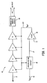
- an automatic gain control (AGC) amplifier of is generally identified by reference numeral 10.
- An input signal is provided at terminal 11 of AGC amplifier 10.
- Amplifier 10 which may be fabricated as a monolithic integrated circuit, comprises amplifier stages A, B, C, and D connected in cascade. Stage D is connected to a single-to-differential converter and buffer circuit 12 that provides an output signal at terminals 13.
- AGC amplifier 10 The gain of AGC amplifier 10 is controlled by a control voltage V agc provided at terminal 14. Control voltage V agc is applied to a linearization circuit 16 which provides an output on line 17 connected to an operational amplifier functioning as a voltage controlled voltage source (VCVS) 18. VCVS 18 provides a conditioned control voltage V agc ′ on line 20 that is fed back to the linearization circuit 16 and applied to each of the amplifier stages A, B, C, and D.
- AGC amplifier 10 is designed so that its overall gain in dB is a linear function of the control voltage V agc at terminal 14. Amplifier 10 has an AGC range of approximately 95 dB at a maximum input power of -4.0 dBm at 50 ohms and an output power of -4.0 dBm at 300 ohms.
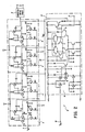
- AGC amplifier 10 is illustrated in a schematic circuit diagram.
- the input signal at terminal 11 is amplified by amplifier stages A, B, C, and D which are connected in a cascade configuration.
- Voltage supply transients are reduced by separating the supply buses for amplifier stages A and B from the buses for stages C and D as shown in FIGURE 2. Because amplifier stages A, B, C, and D are nearly identical, the following description of the operation of amplifier stage A applies similarly to amplifier stages B, C, and D.
- Amplifier stage A is designed around a basic cascode amplifier comprising transistors Q1 and Q2. Cascode amplifier stages are used in the design of linear AGC amplifier 10 because of their high power handling capability, high but stable gain, and gain response capability over a wide dynamic range.
- the input signal at terminal 11 is applied to the base of transistor Q1, which functions as part of a current source for amplifier stage A.
- the current source also includes a complementary transistor Q5, a complementary resistor R2 which equals resistor R1, complementary resistors R3 and R4 which are equal, and resistor R5 which sets the maximum current corresponding to zero automatic gain.
- the complementary components function to reduce current variations due to temperature changes, part tolerances, and manufacturing processes so that an absolute current can be established through the cascode amplifier.
- the corresponding resistors R11, R12, and R15 of stage B; R21, R22, and R25 of stage C; and R31, R32, and R35 of stage D perform similar functions for their respective amplifier stages but have values that are scaled to provide the desired overall gain of AGC amplifier 10.
- Automatic gain control of the cascode amplifier stage A is implemented by transistor Q3 connected in parallel with transistor Q2.
- a conditioned control voltage V agc ′ which is described below, is applied to the base of transistor Q3 through divider resistors R6 and R7, which help reduce interaction between the amplifier stages.
- the emitter of transistor Q4 provides the output of amplifier stage A to amplifier stage B, with inter-stage coupling capacitor C1 provided to limit potential feedback between stages.
- the maximum gain of amplifier stage A is achieved when the conditioned control voltage at the base of transistor Q3 is at a minimum. As the conditioned control voltage increases, transistor Q3 draws current away from transistor Q2, thus lowering the gain of amplifier stage A.
- Diode D1 prevents transistor Q4 from having zero base-collector voltage at minimum gain conditions and prevents collector-emitter breakdown of transistor Q3.
- Amplifier stages B, C, and D function similarly to stage A to control the overall gain of AGC amplifier 10.
- the output from stage D is applied to a single-to-differential converter and buffer circuit 12 which provides an output signal on terminals 13.
- Linearization of AGC amplifier 10 is implemented by providing the control voltage V agc at terminal 14 to the linearization circuit 16.
- the linearizer portion of linearization circuit 16 includes transistors Q11 and Q12, which are large bipolar NPN transistors. The large emitter areas of transistors Q11 and Q12 help to reduce non-linearities at high current densities because of their lower resistance.
- Control voltage V agc which ranges from zero to 4 volts, is applied to the base of transistor Q11.
- the voltage V agc is inverted at the collector of transistor Q11 and also at the base of transistor Q12.
- a rise in V agc results in a linear fall in the base-emitter voltage of transistor Q12.
- This linear change in the base-emitter voltage produces an exponential change in the collector current of transistor Q12.
- the purpose of the linearization circuit 16 is to keep this linear base-emitter voltage as linear as possible over a range of several decades to produce the desired collector current. This circuit forms the basis for the gain control of the entire AGC amplifier 10.
- the linearization circuit 16 includes a pseudo-cascode circuit that imitates the cascode amplifiers, such as described above in amplifier stage A.
- the lower portion of linearization circuit 16, which includes transistors Q13-17, is a psuedo-cascode stage.
- Transistors Q15 and Q17 function as a current source similar to transistors Q1 and Q5 of amplifier stage A.
- the current source circuit including transistors Q15 and Q17 is identical to the linearizer comprising transistors Q11 and Q12 so that both circuits will track together.
- the current source circuit must always be able to provide more current than the linearizer demands. If this were not true, there would be a flat spot in the AGC response curve.
- the pseudo-cascode circuit is provided with the conditioned control voltage V agc ′ as a feedback signal applied to the base of transistor Q14 so that the current source of the linearization circuit 16 imitates the cascode amplifier stages by maintaining a fixed current.
- VCVS 18 produces conditioned control voltage V agc ′, which is a non-linear function of the input control voltage V agc .
- Conditioned control voltage V agc ′ is output on line 20, fed back to linearization circuit 16, and provided to each of the cascode amplifier stages A, B, C, and D.
- Terminal 21 of VCVS 18 is connected to an external capacitor that sets a dominant pole to provide stability for VCVS 18.
- an increase in control voltage V agc at terminal 14 causes the voltage at the base of transistor Q12 to decrease.
- a small decrease in the voltage at the emitter of transistor Q12, which is functionally related to the increase in the control voltage V agc is provided to VCVS 18 on line 17.
- the voltage on line 17 is amplified, inverted, and level shifted by VCVS 18 and output on line 20 as conditioned voltage V agc ′.
- Conditioned voltage V agc ′ is fed back to linearization circuit 16 and provided to the base of transistor Q3 in each of the amplifier stages.
- AGC amplifier 10 provides a linear gain in dB in response to change in the control voltage.
- the output of amplifier stage D is applied to a single-to-differential converter and buffer circuit 12 to limit the output power to -4.0 dBm at 300 ohms.
- AGC amplifier 10 illustrated in FIGURE 2 produces a maximum gain of approximately 65 dB at a control voltage V agc of zero.
- Amplifier 10 has an AGC linear dynamic range of approximately 95 dB with a gain reduction per volt of approximately 30 dB/volt.
- the AGC amplifier of the present invention may also be configured as a differential amplifier.
- an additional cascode amplifier comprising transistors Q1, Q2, and Q3, is connected in each stage of amplifier 10 to form a differential amplifier as is well known in the art.
Landscapes
- Control Of Amplification And Gain Control (AREA)
- Amplifiers (AREA)
Applications Claiming Priority (2)
| Application Number | Priority Date | Filing Date | Title |
|---|---|---|---|
| US07/166,357 US4816772A (en) | 1988-03-09 | 1988-03-09 | Wide range linear automatic gain control amplifier |
| US166357 | 1988-03-09 |
Publications (3)
| Publication Number | Publication Date |
|---|---|
| EP0332367A2 true EP0332367A2 (de) | 1989-09-13 |
| EP0332367A3 EP0332367A3 (de) | 1991-01-30 |
| EP0332367B1 EP0332367B1 (de) | 1996-08-28 |
Family
ID=22602944
Family Applications (1)
| Application Number | Title | Priority Date | Filing Date |
|---|---|---|---|
| EP89302207A Expired - Lifetime EP0332367B1 (de) | 1988-03-09 | 1989-03-06 | Verstärker mit über einen grossen Bereich linearer selbsttätiger Verstärkungsregelung |
Country Status (3)
| Country | Link |
|---|---|
| US (1) | US4816772A (de) |
| EP (1) | EP0332367B1 (de) |
| JP (1) | JPH0720034B2 (de) |
Cited By (1)
| Publication number | Priority date | Publication date | Assignee | Title |
|---|---|---|---|---|
| WO2001048915A3 (en) * | 1999-12-24 | 2001-12-27 | Ericsson Telefon Ab L M | Electronic circuit |
Families Citing this family (43)
| Publication number | Priority date | Publication date | Assignee | Title |
|---|---|---|---|---|
| US5283536A (en) * | 1990-11-30 | 1994-02-01 | Qualcomm Incorporated | High dynamic range closed loop automatic gain control circuit |
| FR2672750B1 (fr) * | 1991-02-08 | 1996-12-20 | Thomson Composants Militaires | Circuit d'amplification a commande de gain exponentielle. |
| US5394113A (en) * | 1992-08-28 | 1995-02-28 | Harris Corporation | High impedance low-distortion linear amplifier |
| US5872481A (en) * | 1995-12-27 | 1999-02-16 | Qualcomm Incorporated | Efficient parallel-stage power amplifier |
| US5974041A (en) * | 1995-12-27 | 1999-10-26 | Qualcomm Incorporated | Efficient parallel-stage power amplifier |
| JP3479405B2 (ja) * | 1996-03-29 | 2003-12-15 | アルプス電気株式会社 | 送信機の増幅回路 |
| US6069525A (en) * | 1997-04-17 | 2000-05-30 | Qualcomm Incorporated | Dual-mode amplifier with high efficiency and high linearity |
| JP2000031763A (ja) * | 1998-07-14 | 2000-01-28 | Fujitsu Ltd | 可変利得回路 |
| US6069526A (en) * | 1998-08-04 | 2000-05-30 | Qualcomm Incorporated | Partial or complete amplifier bypass |
| US6265905B1 (en) | 1999-04-27 | 2001-07-24 | International Business Machines Corporation | Quasi-voltage sensing input impedance controlled preamplifier for magnetoresistive elements |
| JP2001144563A (ja) * | 1999-11-17 | 2001-05-25 | Nec Corp | 可変利得増幅装置 |
| KR100356022B1 (ko) * | 1999-11-23 | 2002-10-18 | 한국전자통신연구원 | 씨모스 가변이득 앰프 및 그 제어 방법 |
| US6684065B2 (en) * | 1999-12-20 | 2004-01-27 | Broadcom Corporation | Variable gain amplifier for low voltage applications |
| JP3748371B2 (ja) * | 2000-09-14 | 2006-02-22 | 株式会社東芝 | 指数変換回路及びこれを用いた可変利得回路 |
| US6559717B1 (en) | 2001-06-13 | 2003-05-06 | Lsi Logic Corporation | Method and/or architecture for implementing a variable gain amplifier control |
| US7171170B2 (en) | 2001-07-23 | 2007-01-30 | Sequoia Communications | Envelope limiting for polar modulators |
| US6985703B2 (en) | 2001-10-04 | 2006-01-10 | Sequoia Corporation | Direct synthesis transmitter |
| US6583667B1 (en) | 2001-12-20 | 2003-06-24 | Institute Of Microelectronics | High frequency CMOS differential amplifiers with fully compensated linear-in-dB variable gain characteristic |
| US6934520B2 (en) * | 2002-02-21 | 2005-08-23 | Semiconductor Components Industries, L.L.C. | CMOS current mode RF detector and method |
| US7489916B1 (en) | 2002-06-04 | 2009-02-10 | Sequoia Communications | Direct down-conversion mixer architecture |
| US6747516B2 (en) * | 2002-10-30 | 2004-06-08 | Analog Devices, Inc. | Power controller circuit for a power amplifier stage |
| US7450915B1 (en) * | 2003-12-27 | 2008-11-11 | Sequoia Communications | Smart transmitter system |
| US7496338B1 (en) * | 2003-12-29 | 2009-02-24 | Sequoia Communications | Multi-segment gain control system |
| US7609118B1 (en) | 2003-12-29 | 2009-10-27 | Sequoia Communications | Phase-locked loop calibration system |
| US7522017B1 (en) | 2004-04-21 | 2009-04-21 | Sequoia Communications | High-Q integrated RF filters |
| US7672648B1 (en) | 2004-06-26 | 2010-03-02 | Quintics Holdings | System for linear amplitude modulation |
| US7548122B1 (en) | 2005-03-01 | 2009-06-16 | Sequoia Communications | PLL with switched parameters |
| US7479815B1 (en) | 2005-03-01 | 2009-01-20 | Sequoia Communications | PLL with dual edge sensitivity |
| US7675379B1 (en) | 2005-03-05 | 2010-03-09 | Quintics Holdings | Linear wideband phase modulation system |
| US7595626B1 (en) | 2005-05-05 | 2009-09-29 | Sequoia Communications | System for matched and isolated references |
| JP2006332797A (ja) * | 2005-05-23 | 2006-12-07 | Niigata Seimitsu Kk | 自動利得制御回路 |
| US7342451B2 (en) * | 2005-08-05 | 2008-03-11 | Siemens Medical Soluitions Usa, Inc. | System for logarithmically controlling multiple variable gain amplifiers |
| US7477103B2 (en) * | 2005-08-05 | 2009-01-13 | Siemens Medical Solutions Usa, Inc. | Amplifier circuit |
| US20070205200A1 (en) * | 2006-03-02 | 2007-09-06 | Brain Box Concepts | Soap bar holder and method of supporting a soap bar |
| US7974374B2 (en) | 2006-05-16 | 2011-07-05 | Quintic Holdings | Multi-mode VCO for direct FM systems |
| US7679468B1 (en) | 2006-07-28 | 2010-03-16 | Quintic Holdings | KFM frequency tracking system using a digital correlator |
| US7522005B1 (en) | 2006-07-28 | 2009-04-21 | Sequoia Communications | KFM frequency tracking system using an analog correlator |
| US7894545B1 (en) | 2006-08-14 | 2011-02-22 | Quintic Holdings | Time alignment of polar transmitter |
| US7920033B1 (en) | 2006-09-28 | 2011-04-05 | Groe John B | Systems and methods for frequency modulation adjustment |
| US8536950B2 (en) * | 2009-08-03 | 2013-09-17 | Qualcomm Incorporated | Multi-stage impedance matching |
| US8102205B2 (en) | 2009-08-04 | 2012-01-24 | Qualcomm, Incorporated | Amplifier module with multiple operating modes |
| KR101862708B1 (ko) | 2011-12-28 | 2018-05-31 | 삼성전자주식회사 | 무선송신기에서 구동증폭기 이득을 지수적으로 제어하기 위한 장치 및 방법 |
| CN103475327A (zh) * | 2013-09-12 | 2013-12-25 | 贵州航天电子科技有限公司 | 一种宽带大动态范围agc中频放大器 |
Family Cites Families (17)
| Publication number | Priority date | Publication date | Assignee | Title |
|---|---|---|---|---|
| US3469195A (en) * | 1965-11-29 | 1969-09-23 | Rca Corp | Detector and agc circuit stabilization responsive to power supply changes |
| DE2060192C3 (de) * | 1970-12-08 | 1978-04-13 | Robert Bosch Gmbh, 7000 Stuttgart | Schaltungsanordnung zur verzögerungsfreien Verstärkungssteuerung |
| US3665507A (en) * | 1971-01-04 | 1972-05-23 | Gen Electric | Signal processor for reception of amplitude or frequency modulated signals |
| NL166162C (nl) * | 1971-05-14 | 1981-06-15 | Philips Nv | Versterkerschakeling met regelbare versterking. |
| JPS5549450B2 (de) * | 1973-01-12 | 1980-12-12 | ||
| GB1546672A (en) * | 1975-07-03 | 1979-05-31 | Sony Corp | Signal compression and expansion circuits |
| JPS5280767A (en) * | 1975-12-27 | 1977-07-06 | Pioneer Electronic Corp | Voltage controlled gain controller |
| JPS5321553A (en) * | 1976-08-11 | 1978-02-28 | Pioneer Electronic Corp | Voltage controlled amplifier |
| US4084187A (en) * | 1976-09-07 | 1978-04-11 | Tektronix, Inc. | Circuit for accurately extracting the synchronization information contained within a composite video waveform |
| DE2803204C2 (de) * | 1978-01-25 | 1983-04-07 | Siemens AG, 1000 Berlin und 8000 München | Verstärker für elektrische Signale |
| US4380711A (en) * | 1980-12-15 | 1983-04-19 | Rockwell International Corporation | Linearization circuit |
| US4426625A (en) * | 1981-08-27 | 1984-01-17 | Rca Corporation | Circuit for linearly gain controlling a differential amplifier |
| DE3204217A1 (de) * | 1982-02-08 | 1983-08-18 | Philips Patentverwaltung Gmbh, 2000 Hamburg | Schaltung zur elektronischen verstaerkungsstellung |
| JPH0744417B2 (ja) * | 1982-11-27 | 1995-05-15 | 株式会社東芝 | ノイズキャンセル回路 |
| NL8400495A (nl) * | 1984-02-16 | 1985-09-16 | Philips Nv | In versterking geregelde versterkerinrichting. |
| DE3540752A1 (de) * | 1985-11-16 | 1987-05-21 | Blaupunkt Werke Gmbh | Schaltungsanordnung mit steuerbarem verstaerkungsfaktor |
| DE3606702A1 (de) * | 1986-03-01 | 1987-09-10 | Ant Nachrichtentech | Regelbarer hf-verstaerker mit linearer stellkennlinie |
-
1988
- 1988-03-09 US US07/166,357 patent/US4816772A/en not_active Expired - Fee Related
-
1989
- 1989-03-06 EP EP89302207A patent/EP0332367B1/de not_active Expired - Lifetime
- 1989-03-08 JP JP1055978A patent/JPH0720034B2/ja not_active Expired - Lifetime
Cited By (1)
| Publication number | Priority date | Publication date | Assignee | Title |
|---|---|---|---|---|
| WO2001048915A3 (en) * | 1999-12-24 | 2001-12-27 | Ericsson Telefon Ab L M | Electronic circuit |
Also Published As
| Publication number | Publication date |
|---|---|
| US4816772A (en) | 1989-03-28 |
| EP0332367A3 (de) | 1991-01-30 |
| JPH0720034B2 (ja) | 1995-03-06 |
| EP0332367B1 (de) | 1996-08-28 |
| JPH01272308A (ja) | 1989-10-31 |
Similar Documents
| Publication | Publication Date | Title |
|---|---|---|
| US4816772A (en) | Wide range linear automatic gain control amplifier | |
| US6049251A (en) | Wide-dynamic-range variable-gain amplifier | |
| US6229374B1 (en) | Variable gain amplifiers and methods having a logarithmic gain control function | |
| US4263562A (en) | High input impedance transistor amplifier | |
| GB2149600A (en) | Improvements in or relating to transistor amplifying and mixing input stages for radio receivers | |
| US5844443A (en) | Linear high-frequency amplifier with high input impedance and high power efficiency | |
| US3786362A (en) | Balanced output operational amplifier | |
| US20040201421A1 (en) | Apparatus, methods and articles of manufacture for power amplifier control in a communication system | |
| EP1928087B1 (de) | Schaltung eines variablen Leistungsverstärkers | |
| US6480066B1 (en) | Amplifiers | |
| US5382919A (en) | Wideband constant impedance amplifiers | |
| JP2005101733A (ja) | バイアス回路 | |
| JPS63164604A (ja) | 増幅回路配置 | |
| EP0387951A1 (de) | Stromverstärker | |
| US3962650A (en) | Integrated circuit amplifier having controlled gain and stable quiescent output voltage level | |
| US5159288A (en) | Receiver circuit having first and second amplifiers | |
| US3541465A (en) | Transistor differential amplifier circuit | |
| US10826438B2 (en) | Bias circuit | |
| US20090140808A1 (en) | Gain control circuit | |
| US4366443A (en) | Television intermediate frequency amplifier | |
| US3427560A (en) | Direct current amplifier | |
| US3651420A (en) | Variable gain direct coupled amplifier | |
| US3733558A (en) | Stable low current amplifier | |
| US5218323A (en) | Transistor direct-coupled amplifier | |
| US4330755A (en) | Power-amplifying circuit |
Legal Events
| Date | Code | Title | Description |
|---|---|---|---|
| PUAI | Public reference made under article 153(3) epc to a published international application that has entered the european phase |
Free format text: ORIGINAL CODE: 0009012 |
|
| AK | Designated contracting states |
Kind code of ref document: A2 Designated state(s): FR GB |
|
| PUAL | Search report despatched |
Free format text: ORIGINAL CODE: 0009013 |
|
| AK | Designated contracting states |
Kind code of ref document: A3 Designated state(s): FR GB |
|
| 17P | Request for examination filed |
Effective date: 19910715 |
|
| 17Q | First examination report despatched |
Effective date: 19931102 |
|
| GRAH | Despatch of communication of intention to grant a patent |
Free format text: ORIGINAL CODE: EPIDOS IGRA |
|
| GRAH | Despatch of communication of intention to grant a patent |
Free format text: ORIGINAL CODE: EPIDOS IGRA |
|
| GRAA | (expected) grant |
Free format text: ORIGINAL CODE: 0009210 |
|
| AK | Designated contracting states |
Kind code of ref document: B1 Designated state(s): FR GB |
|
| ET | Fr: translation filed | ||
| PLBE | No opposition filed within time limit |
Free format text: ORIGINAL CODE: 0009261 |
|
| STAA | Information on the status of an ep patent application or granted ep patent |
Free format text: STATUS: NO OPPOSITION FILED WITHIN TIME LIMIT |
|
| 26N | No opposition filed | ||
| PGFP | Annual fee paid to national office [announced via postgrant information from national office to epo] |
Ref country code: GB Payment date: 20010307 Year of fee payment: 13 |
|
| PGFP | Annual fee paid to national office [announced via postgrant information from national office to epo] |
Ref country code: FR Payment date: 20010313 Year of fee payment: 13 |
|
| REG | Reference to a national code |
Ref country code: GB Ref legal event code: IF02 |
|
| PG25 | Lapsed in a contracting state [announced via postgrant information from national office to epo] |
Ref country code: GB Free format text: LAPSE BECAUSE OF NON-PAYMENT OF DUE FEES Effective date: 20020306 |
|
| GBPC | Gb: european patent ceased through non-payment of renewal fee |
Effective date: 20020306 |
|
| PG25 | Lapsed in a contracting state [announced via postgrant information from national office to epo] |
Ref country code: FR Free format text: LAPSE BECAUSE OF NON-PAYMENT OF DUE FEES Effective date: 20021129 |
|
| REG | Reference to a national code |
Ref country code: FR Ref legal event code: ST |