US7894545B1 - Time alignment of polar transmitter - Google Patents
Time alignment of polar transmitter Download PDFInfo
- Publication number
- US7894545B1 US7894545B1 US11/837,983 US83798307A US7894545B1 US 7894545 B1 US7894545 B1 US 7894545B1 US 83798307 A US83798307 A US 83798307A US 7894545 B1 US7894545 B1 US 7894545B1
- Authority
- US
- United States
- Prior art keywords
- signal
- phase
- polar transmitter
- alignment
- alignment module
- Prior art date
- Legal status (The legal status is an assumption and is not a legal conclusion. Google has not performed a legal analysis and makes no representation as to the accuracy of the status listed.)
- Active, expires
Links
Images


Classifications
-
- H—ELECTRICITY
- H04—ELECTRIC COMMUNICATION TECHNIQUE
- H04L—TRANSMISSION OF DIGITAL INFORMATION, e.g. TELEGRAPHIC COMMUNICATION
- H04L27/00—Modulated-carrier systems
- H04L27/32—Carrier systems characterised by combinations of two or more of the types covered by groups H04L27/02, H04L27/10, H04L27/18 or H04L27/26
- H04L27/34—Amplitude- and phase-modulated carrier systems, e.g. quadrature-amplitude modulated carrier systems
- H04L27/36—Modulator circuits; Transmitter circuits
- H04L27/361—Modulation using a single or unspecified number of carriers, e.g. with separate stages of phase and amplitude modulation
Definitions
- the present invention relates generally to radio transmitters using polar modulation.
- Phase modulation schemes are very effective and are therefore widely used in communication systems.
- a simple example of a phase modulation scheme is quaternary phase shift keying (QPSK).
- QPSK quaternary phase shift keying
- This modulation scheme maps two-bit digital data to one of four phase offsets as shown in FIG. 1 a .
- the trajectory of the complex signal intersects these symbols at periodic points in time.
- pulse-shaping filters needed to constrain the frequency spectrum of the signal—introduce some variations as illustrated by FIG. 1 b.
- FIG. 2 shows a typical QPSK (or I/Q) modulator used to generate the complex phase-modulated signal.
- This technique relies on orthogonal signal vectors to realize the phase offsets—an inherently linear technique, since it depends solely on the matching of these orthogonal signals.
- the I/Q modulator provides a straightforward approach to generating phase-modulated signals. But, it's also possible to generate the phase-modulated signals using a polar transmitter such as the one shown in FIG. 3 . This approach reduces circuitry, lowers power consumption, and potentially supports multiple modulation formats. It separately applies the phase and amplitude signals with precise alignment to realize the complex QPSK modulation. Unfortunately, several factors make this alignment very difficult. It would therefore be advantageous to be able to precisely align the phase and amplitude modulation signals.
- the invention relates to a system and method for effecting precise time alignment of modulation signals applied within a polar transmitter.
- a particular aspect of the invention is directed to a polar transmitter system including a direct synthesis modulator and a signal alignment module.
- the direct synthesis modulator is operative to generate an output signal based upon a reference signal.
- the direct synthesis modulator is responsive to an amplitude modulation control signal and a frequency modulation control signal.
- a signal alignment module is configured to apply the amplitude modulation control signal and the frequency modulation control signal to the direct synthesis modulator in accordance with a defined timing relationship.
- the amplitude modulation control signal and the frequency modulation control signal are based upon an input amplitude modulation signal and an input phase or frequency modulation signal, respectively.
- the invention in another aspect pertains to a signal alignment module for use with a polar transmitter.
- the alignment module includes a first latch arrangement which latches an input amplitude modulation signal and a second latch arrangement which latches an input phase or frequency modulation signal.
- a triggering network provides a first timing signal to the first latch arrangement and a second timing signal to the second latch arrangement. The triggering network also establishes a defined time offset between the first timing signal and the second timing signal.
- a further aspect of the invention may be embodied in an alignment apparatus for use with a polar transmitter system.
- the alignment apparatus includes a signal alignment module configured to apply an amplitude modulation control signal and a frequency modulation control signal to the polar transmitter in accordance with a defined timing relationship.
- a time alignment network operatively coupled between an output of the polar transmitter system and the signal alignment module, sets the defined timing relationship.
- the present invention is also directed to an apparatus for adjusting signal time alignment within a polar transmitter system.
- the apparatus includes a signal alignment module operative to apply control signals to the polar transmitter system.
- the apparatus further includes a time alignment network for setting a timing relationship imposed upon the control signals by the signal alignment module.
- the time alignment network includes: a signal source unit coupled to the signal alignment module, a receiver coupled to an output of the polar transmitter system, and a control network coupled between an output of the receiver and the signal alignment module.
- FIG. 1 a shows a constellation diagram that illustrates how QPSK maps two-bit digital data to one of four offsets
- FIG. 1 b illustrates the trajectory of the complex signal for QPSK modulation
- FIG. 2 shows a diagram of a typical I/Q modulator
- FIG. 3 shows a simplified diagram of a polar transmitter
- FIG. 4 shows a PLL that is used to synthesize a radio frequency carrier signal
- FIG. 5 shows a mathematical model of the PLL shown in FIG. 3 ;
- FIG. 6 shows an integration filter
- FIG. 7 a shows one embodiment of a fractional-N PLL using a ⁇ modulator
- FIG. 7 b illustrates the frequency response of the fractional-N PLL shown in FIG. 7 a
- FIG. 8 a illustrates one embodiment of a fractional-N PLL that supports direct frequency or phase modulation
- FIG. 8 b illustrates the frequency response of the direct phase/frequency modulator shown in FIG. 7 a
- FIG. 9 illustrates the envelope variation for filtered QPSK modulation
- FIG. 10 a shows a simplified diagram of an amplitude modulation system using a variable gain amplifier
- FIG. 10 b shows a simplified diagram of an amplitude modulation system using a switched power amplifier, controlled by a dc-dc regulator;
- FIG. 10 c shows a simplified diagram of an amplitude modulation system using feedback to linearize its response
- FIG. 11 a illustrates the spectral regrowth in an EDGE polar transmitter due to 10 nSec timing error
- FIG. 11 b illustrates the spectral regrowth in an WCDMA polar transmitter due to 2.5 nSec timing error
- FIG. 12 a illustrates the performance sensitivity of the EDGE polar transmitter to timing errors
- FIG. 12 b illustrates the performance sensitivity of the WCDMA polar transmitter to timing errors
- FIG. 13 a shows a polar transmitter with timing alignment of the AM and FM signals using a delay-locked loop, in accordance with the present invention
- FIG. 13 b shows a polar transmitter with timing alignment of the AM and FM signals using digital delay, in accordance with the present invention
- FIG. 14 a shows a diagram of a system for adjusting the time alignment of polar transmitters, in accordance with the present invention
- FIG. 14 b illustrates the symbol pattern used to enhance timing errors as part of the alignment system of FIG. 14 a , in accordance with the present invention
- FIG. 14 c illustrates the complex signal trajectory associated with the symbol pattern shown in FIG. 14 b and part of the alignment system of FIG. 14 a , in accordance with the present invention
- FIG. 14 d shows a diagram of the digital signal source that generates the test signal associated with the alignment system of FIG. 14 a , in accordance with the present invention
- FIG. 14 e shows a diagram of an alternate system for adjusting the time alignment of polar transmitters, in accordance with the present invention.
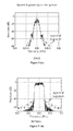
- FIG. 15 a illustrates the frequency spectrum of a polar transmitter driven by the signal source described by FIGS. 14 b - c and part of alignment system of FIG. 14 a , in accordance with the present invention
- FIG. 15 b illustrates the frequency spectrum of a polar transmitter driven by the signal source described by FIGS. 14 b - c and part of alignment system of FIG. 14 a , with a timing error of 2.5 nSec, in accordance with the present invention
- FIG. 16 illustrates the convergence of the alignment adjustment system of FIG. 14 a .
- FIG. 17 a - d illustrate other examples of symbol patterns, similar to FIG. 14 b , that also enhance the timing error as part of the alignment system of FIG. 14 a , in accordance with the present invention.
- a direct synthesis modulator or “polar transmitter” consists of a phase-locked loop (PLL) having a phase/frequency modulation capability followed by an amplitude modulation network.
- PLL phase-locked loop
- FIG. 4 shows a block diagram of a phase-locked loop (PLL), which is used to synthesize a radio frequency carrier. It consists of a voltage-controlled oscillator (VCO), feedback counter (counter), phase/frequency detector (P/FD), charge pump (CP), and integration filter (LPF). This feedback system is further described by the mathematical model shown in FIG. 5 .
- VCO voltage-controlled oscillator
- P/FD phase/frequency detector
- CP charge pump
- LPF integration filter
- the gain K vco describes the relationship between the excess phase of the carrier ⁇ out and the control voltage v ctrl with
- ⁇ out ⁇ ( s ) v ctrl ⁇ ( s ) K vco s
- K vco is in radians/V.
- the VCO drives the feedback counter, which simply divides the output phase ⁇ out by N.
- the phase detector and charge pump circuits generate an output signal i CP that is proportional to the phase difference ⁇ between the two signals applied to the phase detector.
- the output signal i CP can therefore be expressed as
- i CP ⁇ ( s ) K pd ⁇ ⁇ ⁇ ( s ) 2 ⁇ ⁇
- K pd is in A/radians
- ⁇ is in radians.
- a simple integration filter comprising resistor R 1 and capacitors C 1 -C 2 as shown in FIG. 6 , transforms the output signal i CP to the control voltage v ctrl as follows
- T 1 ⁇ ( s ) NK PD ⁇ K VCO ⁇ Z ⁇ ( s ) sN + K PD ⁇ K VCO ⁇ Z ⁇ ( s ) .
- the feedback counter value N effectively sets the output frequency.
- its digital structure restricts N to integer numbers.
- the frequency resolution (or frequency step size) of an integer-N PLL is nominally set by f REF .
- f REF the frequency resolution of an integer-N PLL.
- a fractional-N PLL that uses a ⁇ modulator to develop non-integer values of N is shown in FIG. 7 a .
- the ⁇ modulator advantageously pushes spurious energy (created by the changing values of the feedback counter) to higher frequencies where it can be more effectively attenuated by the PLL's integration filter. It can be shown that the effective value of N is simply the average value described by
- the ⁇ modulator generates the sequence n[x] that satisfies
- ⁇ ⁇ ⁇ f ⁇ ( t ) ( n ⁇ [ x ] - k M )
- ⁇ f REF FM ⁇ ⁇ f REF
- FM is the applied modulation signal.
- the modulation is shaped by the PLL response described by transfer function T 1 (s).
- the PLL's response generally limits the bandwidth of the system so as to attenuate the ⁇ modulator's quantization noise. This is illustrated in FIG. 7 b.
- T 2 ⁇ ( s ) sNK FM sN + K PD ⁇ K VCO ⁇ Z ⁇ ( s ) ⁇ v FM
- K FM is the gain of the VCO port at which the v FM modulating signal is applied.
- the modulation applied to the fractional-N PLL and VCO adjusts the frequency of the output signal of the VCO, not its phase.
- the phase modulation signal ⁇ (t) must be differentiated with
- f c the carrier frequency
- the fractional-N PLL and VCO generate a constant amplitude, phase/frequency-modulated signal centered at the carrier radio frequency. This allows the signal to be amplified using very efficient, compressed amplifiers. Unfortunately, the desired complex transmit signal typically shows envelop variations as illustrated by FIG. 9 . As such, it becomes necessary to modulate the envelope of the phase/frequency-modulated signal to faithfully form the transmit signal.
- VGA variable gain amplifier
- FIG. 10 b shows a second approach. It includes a buffer, driver amplifier, filter, and switched power amplifier supplied by a dc-dc regulator.
- the amplitude modulation is applied through a dc-dc regulator.
- the dc-dc regulator produces an output level V + that tracks the AM signal and consequently restricts the power amplifier's signal swing. It follows that the power amplifier switches between its saturation voltage V sat and 2V + with s(t) ⁇ A(t) ⁇ 1+sign(sin [2 ⁇ (f c +FM)t]) ⁇ +V sat
- a driver amplifier boosts the amplitude of the phase/frequency modulated signal to ensure the switched PA fully switches even at high AM and V + levels.
- the switching operation of the PA produces multiple harmonics that must be attenuated by the its output matching network.
- the dc-dc regulator typically uses large capacitors which unfortunately slow the response to the amplitude modulation input.
- the TXF filter is used to attenuate any wideband noise that could fold in band due to the amplifier's switching response.
- FIG. 10 c shows a third method for amplitude modulation. It consists of a buffer, variable gain amplifier, power amplifier, and feedback network to control the transmitter's output.
- the feedback network linearizes the response to the amplitude modulation signal A(t).
- A(t) the amplitude modulation signal
- the amplitude modulation precisely aligns to the phase/frequency modulation, avoiding spectral regrowth and EVM degradation. Even small timing errors affect the frequency spectrum of the complex transmit signal. This is illustrated in FIG. 11 a for an EDGE polar system with 10 nSec of timing error. The issue becomes more critical for WCDMA as shown in FIG. 11 b . Here, the timing error is only 2 nSec.
- Timing errors also distort the transmitted signal and thereby affect the ability of a receiver to properly detect the message data. This effect is measured by the error vector magnitude (EVM).
- EVM error vector magnitude
- the sensitivity of the modulation system to timing error varies with the symbol rate—making WCDMA systems (3.84 Mcps) much more sensitive than EDGE systems (270 ksps).
- FIG. 12 a shows the sensitivity of EDGE polar transmitters to timing error.
- FIG. 12 b shows the sensitivity of WCDMA polar transmitters to timing error.
- the system shown in FIG. 13 a can align the amplitude modulation to the phase/frequency modulation.
- the system of FIG. 13 a is shown as receiving input amplitude modulation (AM) and frequency modulation (FM) signals, it may also receive an input phase-modulated signal in lieu of an FM signal.
- a simple difference circuit (not shown) is used to compute the derivative of the input phase data.
- the system of FIG. 13( a ) includes a signal alignment module which independently adjusts the timing of the AM and FM input digital data using two latches and a delay locked loop, thereby producing time-aligned AM and FM modulation control data.
- the delay locked loop generates an output signal with selectable delay.
- FIG. 13 b shows another method to generate time-aligned AM and FM modulation control data based upon the input AM and FM digital data.
- the signal alignment module operates digitally to adjust the delay of the input AM signal through a delay equalizer or programmable filter.
- the delay is selected using the time alignment network shown in FIG. 14 a . It generates a test signal that reveals polar modulation timing errors using a simple receiver. The receiver monitors the received signal and adjusts the timing alignment until the signal energy is nulled. The result is near perfect alignment. It is noted that in WCDMA-based embodiments, the transmit signal connects directly to the receiver in the time alignment network through a duplex filter (not shown). In GSM/EDGE-based embodiments, the transmit signal is routed to the receiver using either a switch or RF coupler (not shown).
- test signal is applied and the AM/FM timing is aligned when the transmitter is first activated. In practice, this is sufficient since any delay changes should be small. If needed, the calibration can be repeated in any empty transmission slot.
- the alignment network exploits a special class of complex transmit signals that enhance timing errors.
- This special class of complex transmit signals simply isolates amplitude and phase changes.
- These sequences generate a signal that changes amplitude moving from odd symbols to even symbols and changes phase moving from even symbols to odd symbols.
- the digital signal source interpolates the special complex transmit signal to smooth the frequency and amplitude modulation signals. This results in the complex signal trajectory illustrated in FIG. 14 c .
- the interpolation operation is part of the signal source detailed in FIG. 14 d . This operation effectively up-samples the I/Q data and then filters these signals to limit their bandwidth.
- the resulting data streams are then converted to polar format, FM and AM. Ideally, this signal is unaffected by the low pass filters typically included in the polar transmitter to attenuate wideband noise and D/A converter image signals.
- FIG. 14 e shows an alternative approach to align the AM and FM signals. It is based on the digital delay concept of FIG. 13 b.
- FIG. 15 a The frequency spectrum produced by the polar transmitter operating at a carrier frequency of 825 MHz and with the complex pattern of FIG. 14 b is shown in FIG. 15 a . It generates several frequency tones separated by 1.5 MHz, equal one-half the symbol rate.
- FIG. 15 b shows the same polar transmitter with 2.5 nSec of timing error. The frequency tone at 821.5 MHz grew more than 30 dB. Furthermore, this tone rises as the timing error increases.
- the radio receiver configured to track the 821.5 MHz tone, easily detects the level. It in turn drives the controller to increase/decrease the offset of the delay from the delay-locked loop by selecting different output signals.
- the parabolic shape of FIG. 16 guarantees convergence to the optimal timing for the AM and FM signals.
- the signal source makes detection of the timing error easy. It relies on a newly-defined class of complex transmit signals that simply isolates amplitude and phase changes. Since this is a class of signals, multiple variations are possible, including, but not limited to, FIGS. 14 a and 17 a - d.
- the alignment network properly adjusts the polar transmitter to minimize spectral regrowth and EVM degradation due to timing errors.
Landscapes
- Engineering & Computer Science (AREA)
- Computer Networks & Wireless Communication (AREA)
- Signal Processing (AREA)
- Transmitters (AREA)
Abstract
Description
fVCO=NfREF
where fvco is the frequency of the VCO output signal, N is the value of the feedback counter, and fREF is the frequency of the reference signal.
v out(t)=A cos(ωo t+K vco ∫v ctrl(t)dt)
where ωo is the free-running frequency of the oscillator and Kvco is its associated gain. The gain Kvco describes the relationship between the excess phase of the carrier Φout and the control voltage vctrl with
where Kvco is in radians/V. The VCO drives the feedback counter, which simply divides the output phase Φout by N. When the phase-locked loop is stable, the phase detector and charge pump circuits generate an output signal iCP that is proportional to the phase difference Δθ between the two signals applied to the phase detector. The output signal iCP can therefore be expressed as
where Kpd is in A/radians and Δθ is in radians. A simple integration filter, comprising resistor R1 and capacitors C1-C2 as shown in
where a zero (at 1/R1C1) has been added to stabilize the second order system and the capacitor C2 has been included to reduce any ripple on the control voltage. Combining the above relations yields the closed-loop response of the system to an input signal
where M[x] is the sequence of feedback counter values. This expands to
N[x]=N int +n[x]
where Nint is the integer part and n[x] is the fractional part of N[x]. The ΔΣ modulator generates the sequence n[x] that satisfies
where k is the input to the ΔΣ modulator with resolution M.
f vco =f c +Δf(t)=(N int +n[x])f REF
where Δf(t) is the frequency modulation equal to
and FM is the applied modulation signal. In practice, the modulation is shaped by the PLL response described by transfer function T1(s). The PLL's response generally limits the bandwidth of the system so as to attenuate the ΔΣ modulator's quantization noise. This is illustrated in
where KFM is the gain of the VCO port at which the vFM modulating signal is applied. Ideally, the two expressions combine to yield a flat and uniform response as illustrated in
FMfREF=KFMvFM
where fc is the carrier frequency. Since the phase signal is formed digitally and then converted to analog form, a simple difference circuit is used to compute the derivative of the discrete phase data θ(x)
dθ(x+1)=θ(x+1)−dθ(x)
where x is the sample index and dθ(x) is the difference or derivative.
s(t)=A(t)sin [2π(f c +FM)t]
where A(t) is the amplitude modulation and is always positive. This approach—known as small-signal polar modulation or polar lite—eases design but requires a linear power amplifier. It also minimizes the time delay and associated alignment error between the phase/frequency modulator and the amplitude modulator. In most situations, the TXF filter is included to attenuate receive band noise.
s(t)□A(t){1+sign(sin [2π(fc+FM)t])}+Vsat
A driver amplifier boosts the amplitude of the phase/frequency modulated signal to ensure the switched PA fully switches even at high AM and V+ levels. In practice, the switching operation of the PA produces multiple harmonics that must be attenuated by the its output matching network. To minimize noise, the dc-dc regulator typically uses large capacitors which unfortunately slow the response to the amplitude modulation input. The TXF filter is used to attenuate any wideband noise that could fold in band due to the amplifier's switching response.
I=[r 1,0,0,−r 2 ,−r 1,0,0,r 2] and Q=[0,r 2 ,r 1,0,0,−r 2 ,−r 1,0]
where r1>r2. These sequences generate a signal that changes amplitude moving from odd symbols to even symbols and changes phase moving from even symbols to odd symbols.
Claims (22)
I=[r 1,0,0,−r 2 ,−r 1,0,0,r 2] and Q=[0,r 2 ,r 1,0,0,−r 2 ,−r 1,0]
I=[r 1,0,−r 1,0] and Q=[0,r 2,0,−r 2]
I=[r 1 ,−r 3 ,−r 2 ,−r 3 ,−r 2 ,r 3] and Q=[0,r 5 ,r 4 ,−r 5 ,−r 4,0]
I=[r 1 ,r 2,0,−r 2 ,−r 1 ,−r 2,0,r 2] and Q=[0,r 2 ,r 1 ,r 2,0,−r 2 ,−r 1 ,−r 2,]
I=[r 1 ,r 3 ,r 2 ,r 4,0,−r 4 ,−r 2 ,−r 3 ,−r 1 ,−r 3 ,−r 2 ,−r 4,0,r 4 ,r 2 ,r 3] and Q=[0,r 4 ,r 2 ,r 3 ,r 1 ,r 3 ,r 2 ,r 4,0,−r 4 ,−r 2 ,−r 3 ,−r 1 ,−r 3 ,−r 2 ,−r 4]
Priority Applications (1)
| Application Number | Priority Date | Filing Date | Title |
|---|---|---|---|
| US11/837,983 US7894545B1 (en) | 2006-08-14 | 2007-08-13 | Time alignment of polar transmitter |
Applications Claiming Priority (2)
| Application Number | Priority Date | Filing Date | Title |
|---|---|---|---|
| US82235706P | 2006-08-14 | 2006-08-14 | |
| US11/837,983 US7894545B1 (en) | 2006-08-14 | 2007-08-13 | Time alignment of polar transmitter |
Publications (1)
| Publication Number | Publication Date |
|---|---|
| US7894545B1 true US7894545B1 (en) | 2011-02-22 |
Family
ID=43597142
Family Applications (1)
| Application Number | Title | Priority Date | Filing Date |
|---|---|---|---|
| US11/837,983 Active 2029-06-14 US7894545B1 (en) | 2006-08-14 | 2007-08-13 | Time alignment of polar transmitter |
Country Status (1)
| Country | Link |
|---|---|
| US (1) | US7894545B1 (en) |
Cited By (4)
| Publication number | Priority date | Publication date | Assignee | Title |
|---|---|---|---|---|
| US20100027445A1 (en) * | 2008-08-01 | 2010-02-04 | Toru Matsuura | Transmission circuit, method for determining delay time used in the transmission circuit, and communication apparatus using the transmission circuit |
| US8773200B2 (en) | 2012-07-08 | 2014-07-08 | R2 Semiconductor, Inc. | Decoupling circuits for filtering a voltage supply of multiple power amplifiers |
| US20140354353A1 (en) * | 2011-12-15 | 2014-12-04 | IAD Gesellschaft für Informatik, Automatisierung und Datenverarbeitung mbH | Device having a delta-sigma modulator and a switching amplifier connected thereto |
| US9356609B1 (en) | 2014-12-19 | 2016-05-31 | Telefonaktiebolaget L M Ericsson (Publ) | Phase switching PLL and calibration method |
Citations (110)
| Publication number | Priority date | Publication date | Assignee | Title |
|---|---|---|---|---|
| US4263560A (en) | 1974-06-06 | 1981-04-21 | The United States Of America As Represented By The Secretary Of The Navy | Log-exponential AGC circuit |
| US4430627A (en) | 1978-12-05 | 1984-02-07 | Kenji Machida | Amplitude controlled sine wave oscillator |
| US4769588A (en) | 1987-09-04 | 1988-09-06 | Digital Equipment Corporation | Apparatus and method for providing a current exponentially proportional to voltage and directly proportional to temperature |
| US4816772A (en) | 1988-03-09 | 1989-03-28 | Rockwell International Corporation | Wide range linear automatic gain control amplifier |
| US4926135A (en) | 1988-06-08 | 1990-05-15 | U.S. Philips Corporation | Balanced integrator-filter arrangement |
| US4965531A (en) | 1989-11-22 | 1990-10-23 | Carleton University | Frequency synthesizers having dividing ratio controlled by sigma-delta modulator |
| US5006818A (en) | 1987-10-12 | 1991-04-09 | Kabushiki Kaisha Toshiba | Linear differential amplifier |
| US5015968A (en) | 1990-07-27 | 1991-05-14 | Pacific Monolithics | Feedback cascode amplifier |
| US5030923A (en) | 1988-11-18 | 1991-07-09 | Sanyo Electric Co., Ltd. | Variable gain amplifier |
| US5289136A (en) | 1991-06-04 | 1994-02-22 | Silicon Systems, Inc. | Bipolar differential pair based transconductance element with improved linearity and signal to noise ratio |
| US5331292A (en) | 1992-07-16 | 1994-07-19 | National Semiconductor Corporation | Autoranging phase-lock-loop circuit |
| US5399990A (en) | 1993-02-19 | 1995-03-21 | Mitsubishi Denki Kabushiki Kaisha | Differential amplifier circuit having reduced power supply voltage |
| US5491450A (en) | 1993-06-01 | 1996-02-13 | Martin Marietta Corporation | Low power consumption process-insensitive feedback amplifier |
| US5508660A (en) | 1993-10-05 | 1996-04-16 | International Business Machines Corporation | Charge pump circuit with symmetrical current output for phase-controlled loop system |
| US5548594A (en) | 1993-12-28 | 1996-08-20 | Nec Corporation | Compact AGC circuit with stable characteristics |
| US5561385A (en) | 1994-04-08 | 1996-10-01 | Lg Semicon Co., Ltd. | Internal voltage generator for semiconductor device |
| US5581216A (en) | 1995-01-24 | 1996-12-03 | Ic Works, Inc. | Low jitter voltage controlled oscillator (VCO) circuit |
| US5625325A (en) | 1995-12-22 | 1997-04-29 | Microtune, Inc. | System and method for phase lock loop gain stabilization |
| US5631587A (en) | 1994-05-03 | 1997-05-20 | Pericom Semiconductor Corporation | Frequency synthesizer with adaptive loop bandwidth |
| US5648744A (en) | 1995-12-22 | 1997-07-15 | Microtune, Inc. | System and method for voltage controlled oscillator automatic band selection |
| US5677646A (en) | 1995-12-27 | 1997-10-14 | Maxim Integrated Products, Inc. | Differential pair amplifier with improved linearity in low-voltage applications |
| US5739730A (en) | 1995-12-22 | 1998-04-14 | Microtune, Inc. | Voltage controlled oscillator band switching technique |
| US5767748A (en) | 1996-02-08 | 1998-06-16 | Kabushiki Kaisha Toshiba | Voltage controlled oscillator and voltage controlled delay circuit |
| US5818303A (en) | 1996-11-21 | 1998-10-06 | Fujitsu Limited | Fractional N-frequency synthesizer and spurious signal cancel circuit |
| US5834987A (en) | 1997-07-30 | 1998-11-10 | Ercisson Inc. | Frequency synthesizer systems and methods for three-point modulation with a DC response |
| US5862465A (en) | 1996-01-29 | 1999-01-19 | Oki Electric Industry Co., Ltd. | Hysteresis-free anti-saturation circuit |
| US5878101A (en) | 1996-01-29 | 1999-03-02 | Fujitsu Limited | Swallow counter with modulus signal output control |
| US5880631A (en) | 1996-02-28 | 1999-03-09 | Qualcomm Incorporated | High dynamic range variable gain amplifier |
| US5939922A (en) | 1995-09-13 | 1999-08-17 | Kabushiki Kaisha Toshiba | Input circuit device with low power consumption |
| US5945855A (en) | 1997-08-29 | 1999-08-31 | Adaptec, Inc. | High speed phase lock loop having high precision charge pump with error cancellation |
| US5949286A (en) | 1997-09-26 | 1999-09-07 | Ericsson Inc. | Linear high frequency variable gain amplifier |
| US5990740A (en) | 1997-12-02 | 1999-11-23 | Nokia Mobile Phones | Differential amplifier with adjustable linearity |
| US5994959A (en) | 1998-12-18 | 1999-11-30 | Maxim Integrated Products, Inc. | Linearized amplifier core |
| US5999056A (en) | 1998-06-30 | 1999-12-07 | Philips Electronics North Amercia Corporation | Variable gain amplifier using impedance network |
| US6011437A (en) | 1998-05-04 | 2000-01-04 | Marvell Technology Group, Ltd. | High precision, high bandwidth variable gain amplifier and method |
| US6018651A (en) | 1995-11-29 | 2000-01-25 | Motorola, Inc. | Radio subscriber unit having a switched antenna diversity apparatus and method therefor |
| US6031425A (en) | 1997-07-25 | 2000-02-29 | Fujitsu Limited | Low power prescaler for a PLL circuit |
| US6044124A (en) | 1997-08-22 | 2000-03-28 | Silicon Systems Design Ltd. | Delta sigma PLL with low jitter |
| US6052035A (en) | 1998-03-19 | 2000-04-18 | Microchip Technology Incorporated | Oscillator with clock output inhibition control |
| US6057739A (en) | 1997-09-26 | 2000-05-02 | Advanced Micro Devices, Inc. | Phase-locked loop with variable parameters |
| US6060935A (en) | 1997-10-10 | 2000-05-09 | Lucent Technologies Inc. | Continuous time capacitor-tuner integrator |
| US6091307A (en) | 1998-07-29 | 2000-07-18 | Lucent Techmologies Inc. | Rapid turn-on, controlled amplitude crystal oscillator |
| US6100767A (en) | 1997-09-29 | 2000-08-08 | Sanyo Electric Co., Ltd. | Phase-locked loop with improved trade-off between lock-up time and power dissipation |
| US6114920A (en) | 1997-10-14 | 2000-09-05 | Lucent Technologies Inc. | Self-calibrating voltage-controlled oscillator for asynchronous phase applications |
| US6163207A (en) | 1998-01-07 | 2000-12-19 | U.S. Philips Corporation | Integrator-filter circuit |
| US6173011B1 (en) | 1998-05-28 | 2001-01-09 | Glenayre Electronics, Inc. | Forward-backward channel interpolator |
| US6191956B1 (en) | 1999-09-24 | 2001-02-20 | Honeywell International Inc. | Circuit for generating high voltage to ignite oil or gas or operative neon tubes |
| US6204728B1 (en) | 1999-01-28 | 2001-03-20 | Maxim Integrated Products, Inc. | Radio frequency amplifier with reduced intermodulation distortion |
| US6211737B1 (en) | 1999-07-16 | 2001-04-03 | Philips Electronics North America Corporation | Variable gain amplifier with improved linearity |
| US6229374B1 (en) | 2000-03-23 | 2001-05-08 | International Business Machines Corporation | Variable gain amplifiers and methods having a logarithmic gain control function |
| US6246289B1 (en) | 1999-02-19 | 2001-06-12 | Stmicroelectronics S.R.L. | Variable-gain multistage amplifier with broad bandwidth and reduced phase variations |
| US6255889B1 (en) | 1999-11-09 | 2001-07-03 | Nokia Networks Oy | Mixer using four quadrant multiplier with reactive feedback elements |
| US6259321B1 (en) | 1999-11-23 | 2001-07-10 | Electronics And Telecommunications Research Institute | CMOS variable gain amplifier and control method therefor |
| US6288609B1 (en) | 2000-02-29 | 2001-09-11 | Motorola, Inc. | Gain controllable low noise amplifier with automatic linearity enhancement and method of doing same |
| US6298093B1 (en) | 1999-08-05 | 2001-10-02 | Raytheon Company | Apparatus and method for phase and frequency digital modulation |
| US6333675B1 (en) | 1999-07-22 | 2001-12-25 | Fujitsu Limited | Variable gain amplifier with gain control voltage branch circuit |
| US6370372B1 (en) | 2000-09-25 | 2002-04-09 | Conexant Systems, Inc. | Subharmonic mixer circuit and method |
| US6392487B1 (en) | 2000-08-02 | 2002-05-21 | Rf Micro Devices, Inc | Variable gain amplifier |
| US6404252B1 (en) | 2000-07-31 | 2002-06-11 | National Semiconductor Corporation | No standby current consuming start up circuit |
| US20020071497A1 (en) | 2000-10-31 | 2002-06-13 | Erik Bengtsson | IQ modulation systems and methods that use separate phase and amplitude signal paths and perform modulation within a phase locked loop |
| US20020135428A1 (en) | 2001-03-20 | 2002-09-26 | Broadcom Corporation | Apparatus and method for phase lock loop gain control using unit current sources |
| US6476660B1 (en) | 1998-07-29 | 2002-11-05 | Nortel Networks Limited | Fully integrated long time constant integrator circuit |
| US20020193009A1 (en) | 2000-07-31 | 2002-12-19 | Tensolite Company | Cable structure with improved termination connector |
| US6515553B1 (en) | 1999-09-10 | 2003-02-04 | Conexant Systems Inc. | Delta-sigma based dual-port modulation scheme and calibration techniques for similar modulation schemes |
| US20030078016A1 (en) | 2001-10-04 | 2003-04-24 | Groe John B. | Direct synthesis transmitter |
| US6560448B1 (en) | 2000-10-02 | 2003-05-06 | Intersil Americas Inc. | DC compensation system for a wireless communication device configured in a zero intermediate frequency architecture |
| US6559717B1 (en) | 2001-06-13 | 2003-05-06 | Lsi Logic Corporation | Method and/or architecture for implementing a variable gain amplifier control |
| US20030092405A1 (en) | 2001-07-23 | 2003-05-15 | Groe John B. | Envelope limiting for polar modulators |
| US6571083B1 (en) | 1999-05-05 | 2003-05-27 | Motorola, Inc. | Method and apparatus for automatic simulcast correction for a correlation detector |
| US6577190B2 (en) | 2000-10-31 | 2003-06-10 | Hynix Semiconductor, Inc. | Linear gain control amplifier |
| US6583671B2 (en) | 2000-12-01 | 2003-06-24 | Sony Corporation | Stable AGC transimpedance amplifier with expanded dynamic range |
| US20030118143A1 (en) | 2001-12-26 | 2003-06-26 | Texas Instruments Incorporated | Direct modulation architecture for amplitude and phase modulated signals in multi-mode signal transmission |
| US20030197564A1 (en) | 2002-04-22 | 2003-10-23 | Humphreys Scott Robert | Coarse tuning for fractional-n synthesizers |
| US6639474B2 (en) | 2000-12-22 | 2003-10-28 | Nokia Corporation | Adjustable oscillator |
| US6664865B2 (en) | 2001-05-11 | 2003-12-16 | Sequoia Communications | Amplitude-adjustable oscillator |
| US6683509B2 (en) | 2001-08-21 | 2004-01-27 | Zarlink Semiconductor Limited | Voltage controlled oscillators |
| US20040017852A1 (en) | 2002-05-29 | 2004-01-29 | Diego Garrido | Predictive interpolation of a video signal |
| US6693977B2 (en) | 1997-05-13 | 2004-02-17 | Matsushita Electric Industrial Co., Ltd. | Portable radio device with direct conversion receiver including mixer down-converting incoming signal, and demodulator operating on downconverted signal |
| US6703887B2 (en) | 2001-08-31 | 2004-03-09 | Sequoia Communications | Long time-constant integrator |
| US20040051590A1 (en) | 2000-07-10 | 2004-03-18 | Silicon Laboratories, Inc. | Digitally-synthesized loop filter circuit particularly useful for a phase locked loop |
| US6711391B1 (en) | 2000-10-10 | 2004-03-23 | Qualcomm, Incorporated | Gain linearizer for variable gain amplifiers |
| US6724235B2 (en) | 2001-07-23 | 2004-04-20 | Sequoia Communications | BiCMOS variable-gain transconductance amplifier |
| US6734736B2 (en) | 2001-12-28 | 2004-05-11 | Texas Instruments Incorporated | Low power variable gain amplifier |
| US6744319B2 (en) | 2001-12-13 | 2004-06-01 | Hynix Semiconductor Inc. | Exponential function generator embodied by using a CMOS process and variable gain amplifier employing the same |
| US6751272B1 (en) | 1998-02-11 | 2004-06-15 | 3Com Corporation | Dynamic adjustment to preserve signal-to-noise ratio in a quadrature detector system |
| US6753738B1 (en) | 2001-06-25 | 2004-06-22 | Silicon Laboratories, Inc. | Impedance tuning circuit |
| US6763228B2 (en) | 2001-01-02 | 2004-07-13 | Intersil Americas, Inc. | Precision automatic gain control circuit |
| US6774740B1 (en) | 2002-04-19 | 2004-08-10 | Sequoia Communications Corp. | System for highly linear phase modulation |
| US6777999B2 (en) | 2000-09-14 | 2004-08-17 | Kabushiki Kaisha Toshiba | Exponential conversion circuit and variable gain circuit |
| US6781425B2 (en) | 2001-09-04 | 2004-08-24 | Atheros Communications, Inc. | Current-steering charge pump circuit and method of switching |
| US6795843B1 (en) | 2000-11-08 | 2004-09-21 | Sequoia Communications | Low-distortion differential circuit |
| US6798290B2 (en) | 2001-08-31 | 2004-09-28 | Sequoia Communications | Translinear variable gain amplifier |
| US6801089B2 (en) | 2001-05-04 | 2004-10-05 | Sequoia Communications | Continuous variable-gain low-noise amplifier |
| US6845139B2 (en) | 2002-08-23 | 2005-01-18 | Dsp Group, Inc. | Co-prime division prescaler and frequency synthesizer |
| US6856205B1 (en) | 2002-04-17 | 2005-02-15 | Sequoia Communications | VCO with automatic calibration |
| US6870411B2 (en) | 2001-08-30 | 2005-03-22 | Renesas Technology Corp. | Phase synchronizing circuit |
| US6917719B2 (en) | 1998-06-26 | 2005-07-12 | Sarnoff Corporation | Method and apparatus for region-based allocation of processing resources and control of input image formation |
| US6940356B2 (en) | 2003-02-14 | 2005-09-06 | Fairchild Semiconductor Corporation | Circuitry to reduce PLL lock acquisition time |
| US6943600B2 (en) | 2002-12-23 | 2005-09-13 | Stmicroelectronics Belgium Nv | Delay-compensated fractional-N frequency synthesizer |
| US6975687B2 (en) | 2000-06-16 | 2005-12-13 | Hughes Electronics Corporation | Linearized offset QPSK modulation utilizing a sigma-delta based frequency modulator |
| US20060003720A1 (en) | 2004-02-20 | 2006-01-05 | Lee Kang Y | System and method for tuning a frequency generator using an LC oscillator |
| US6990327B2 (en) | 2003-04-30 | 2006-01-24 | Agency For Science Technology And Research | Wideband monolithic tunable high-Q notch filter for image rejection in RF application |
| US7062248B2 (en) | 2003-01-16 | 2006-06-13 | Nokia Corporation | Direct conversion receiver having a low pass pole implemented with an active low pass filter |
| US7065334B1 (en) | 2000-09-28 | 2006-06-20 | Kabushiki Kaisha Toshiba | Variable gain amplifier device |
| US7088979B1 (en) | 2001-06-13 | 2006-08-08 | Lsi Logic Corporation | Triple conversion RF tuner with synchronous local oscillators |
| US7123102B2 (en) | 2003-09-29 | 2006-10-17 | Renesas Technology Corporation | Wireless communication semiconductor integrated circuit device and mobile communication system |
| US7142062B2 (en) | 2004-12-30 | 2006-11-28 | Nokia Corporation | VCO center frequency tuning and limiting gain variation |
| US7148764B2 (en) | 2001-11-16 | 2006-12-12 | Renesas Technology Corp. | Communication semiconductor integrated circuit device and a wireless communication system |
| US7215215B2 (en) | 2004-03-15 | 2007-05-08 | Matsushita Electric Industrial Co., Ltd. | Phase modulation apparatus, polar modulation transmission apparatus, wireless transmission apparatus and wireless communication apparatus |
| US20070275676A1 (en) * | 2006-04-07 | 2007-11-29 | Broadcom Corporation, A California Corporation | DAC based switching power amplifier |
-
2007
- 2007-08-13 US US11/837,983 patent/US7894545B1/en active Active
Patent Citations (115)
| Publication number | Priority date | Publication date | Assignee | Title |
|---|---|---|---|---|
| US4263560A (en) | 1974-06-06 | 1981-04-21 | The United States Of America As Represented By The Secretary Of The Navy | Log-exponential AGC circuit |
| US4430627A (en) | 1978-12-05 | 1984-02-07 | Kenji Machida | Amplitude controlled sine wave oscillator |
| US4769588A (en) | 1987-09-04 | 1988-09-06 | Digital Equipment Corporation | Apparatus and method for providing a current exponentially proportional to voltage and directly proportional to temperature |
| US5006818A (en) | 1987-10-12 | 1991-04-09 | Kabushiki Kaisha Toshiba | Linear differential amplifier |
| US4816772A (en) | 1988-03-09 | 1989-03-28 | Rockwell International Corporation | Wide range linear automatic gain control amplifier |
| US4926135A (en) | 1988-06-08 | 1990-05-15 | U.S. Philips Corporation | Balanced integrator-filter arrangement |
| US5030923A (en) | 1988-11-18 | 1991-07-09 | Sanyo Electric Co., Ltd. | Variable gain amplifier |
| US4965531A (en) | 1989-11-22 | 1990-10-23 | Carleton University | Frequency synthesizers having dividing ratio controlled by sigma-delta modulator |
| US5015968A (en) | 1990-07-27 | 1991-05-14 | Pacific Monolithics | Feedback cascode amplifier |
| US5289136A (en) | 1991-06-04 | 1994-02-22 | Silicon Systems, Inc. | Bipolar differential pair based transconductance element with improved linearity and signal to noise ratio |
| US5331292A (en) | 1992-07-16 | 1994-07-19 | National Semiconductor Corporation | Autoranging phase-lock-loop circuit |
| US5399990A (en) | 1993-02-19 | 1995-03-21 | Mitsubishi Denki Kabushiki Kaisha | Differential amplifier circuit having reduced power supply voltage |
| US5491450A (en) | 1993-06-01 | 1996-02-13 | Martin Marietta Corporation | Low power consumption process-insensitive feedback amplifier |
| US5508660A (en) | 1993-10-05 | 1996-04-16 | International Business Machines Corporation | Charge pump circuit with symmetrical current output for phase-controlled loop system |
| US5548594A (en) | 1993-12-28 | 1996-08-20 | Nec Corporation | Compact AGC circuit with stable characteristics |
| US5561385A (en) | 1994-04-08 | 1996-10-01 | Lg Semicon Co., Ltd. | Internal voltage generator for semiconductor device |
| US5631587A (en) | 1994-05-03 | 1997-05-20 | Pericom Semiconductor Corporation | Frequency synthesizer with adaptive loop bandwidth |
| US5581216A (en) | 1995-01-24 | 1996-12-03 | Ic Works, Inc. | Low jitter voltage controlled oscillator (VCO) circuit |
| US5939922A (en) | 1995-09-13 | 1999-08-17 | Kabushiki Kaisha Toshiba | Input circuit device with low power consumption |
| US6018651A (en) | 1995-11-29 | 2000-01-25 | Motorola, Inc. | Radio subscriber unit having a switched antenna diversity apparatus and method therefor |
| US5648744A (en) | 1995-12-22 | 1997-07-15 | Microtune, Inc. | System and method for voltage controlled oscillator automatic band selection |
| US5739730A (en) | 1995-12-22 | 1998-04-14 | Microtune, Inc. | Voltage controlled oscillator band switching technique |
| US5625325A (en) | 1995-12-22 | 1997-04-29 | Microtune, Inc. | System and method for phase lock loop gain stabilization |
| US5677646A (en) | 1995-12-27 | 1997-10-14 | Maxim Integrated Products, Inc. | Differential pair amplifier with improved linearity in low-voltage applications |
| US5878101A (en) | 1996-01-29 | 1999-03-02 | Fujitsu Limited | Swallow counter with modulus signal output control |
| US5862465A (en) | 1996-01-29 | 1999-01-19 | Oki Electric Industry Co., Ltd. | Hysteresis-free anti-saturation circuit |
| US5767748A (en) | 1996-02-08 | 1998-06-16 | Kabushiki Kaisha Toshiba | Voltage controlled oscillator and voltage controlled delay circuit |
| US5880631A (en) | 1996-02-28 | 1999-03-09 | Qualcomm Incorporated | High dynamic range variable gain amplifier |
| US5818303A (en) | 1996-11-21 | 1998-10-06 | Fujitsu Limited | Fractional N-frequency synthesizer and spurious signal cancel circuit |
| US6693977B2 (en) | 1997-05-13 | 2004-02-17 | Matsushita Electric Industrial Co., Ltd. | Portable radio device with direct conversion receiver including mixer down-converting incoming signal, and demodulator operating on downconverted signal |
| US6031425A (en) | 1997-07-25 | 2000-02-29 | Fujitsu Limited | Low power prescaler for a PLL circuit |
| US5834987A (en) | 1997-07-30 | 1998-11-10 | Ercisson Inc. | Frequency synthesizer systems and methods for three-point modulation with a DC response |
| US6044124A (en) | 1997-08-22 | 2000-03-28 | Silicon Systems Design Ltd. | Delta sigma PLL with low jitter |
| US5945855A (en) | 1997-08-29 | 1999-08-31 | Adaptec, Inc. | High speed phase lock loop having high precision charge pump with error cancellation |
| US6057739A (en) | 1997-09-26 | 2000-05-02 | Advanced Micro Devices, Inc. | Phase-locked loop with variable parameters |
| US5949286A (en) | 1997-09-26 | 1999-09-07 | Ericsson Inc. | Linear high frequency variable gain amplifier |
| US6100767A (en) | 1997-09-29 | 2000-08-08 | Sanyo Electric Co., Ltd. | Phase-locked loop with improved trade-off between lock-up time and power dissipation |
| US6060935A (en) | 1997-10-10 | 2000-05-09 | Lucent Technologies Inc. | Continuous time capacitor-tuner integrator |
| US6114920A (en) | 1997-10-14 | 2000-09-05 | Lucent Technologies Inc. | Self-calibrating voltage-controlled oscillator for asynchronous phase applications |
| US5990740A (en) | 1997-12-02 | 1999-11-23 | Nokia Mobile Phones | Differential amplifier with adjustable linearity |
| US6163207A (en) | 1998-01-07 | 2000-12-19 | U.S. Philips Corporation | Integrator-filter circuit |
| US6751272B1 (en) | 1998-02-11 | 2004-06-15 | 3Com Corporation | Dynamic adjustment to preserve signal-to-noise ratio in a quadrature detector system |
| US6052035A (en) | 1998-03-19 | 2000-04-18 | Microchip Technology Incorporated | Oscillator with clock output inhibition control |
| US6011437A (en) | 1998-05-04 | 2000-01-04 | Marvell Technology Group, Ltd. | High precision, high bandwidth variable gain amplifier and method |
| US6173011B1 (en) | 1998-05-28 | 2001-01-09 | Glenayre Electronics, Inc. | Forward-backward channel interpolator |
| US6917719B2 (en) | 1998-06-26 | 2005-07-12 | Sarnoff Corporation | Method and apparatus for region-based allocation of processing resources and control of input image formation |
| US5999056A (en) | 1998-06-30 | 1999-12-07 | Philips Electronics North Amercia Corporation | Variable gain amplifier using impedance network |
| US6476660B1 (en) | 1998-07-29 | 2002-11-05 | Nortel Networks Limited | Fully integrated long time constant integrator circuit |
| US6091307A (en) | 1998-07-29 | 2000-07-18 | Lucent Techmologies Inc. | Rapid turn-on, controlled amplitude crystal oscillator |
| US5994959A (en) | 1998-12-18 | 1999-11-30 | Maxim Integrated Products, Inc. | Linearized amplifier core |
| US6204728B1 (en) | 1999-01-28 | 2001-03-20 | Maxim Integrated Products, Inc. | Radio frequency amplifier with reduced intermodulation distortion |
| US6246289B1 (en) | 1999-02-19 | 2001-06-12 | Stmicroelectronics S.R.L. | Variable-gain multistage amplifier with broad bandwidth and reduced phase variations |
| US6571083B1 (en) | 1999-05-05 | 2003-05-27 | Motorola, Inc. | Method and apparatus for automatic simulcast correction for a correlation detector |
| US6211737B1 (en) | 1999-07-16 | 2001-04-03 | Philips Electronics North America Corporation | Variable gain amplifier with improved linearity |
| US6333675B1 (en) | 1999-07-22 | 2001-12-25 | Fujitsu Limited | Variable gain amplifier with gain control voltage branch circuit |
| US6298093B1 (en) | 1999-08-05 | 2001-10-02 | Raytheon Company | Apparatus and method for phase and frequency digital modulation |
| US6515553B1 (en) | 1999-09-10 | 2003-02-04 | Conexant Systems Inc. | Delta-sigma based dual-port modulation scheme and calibration techniques for similar modulation schemes |
| US6191956B1 (en) | 1999-09-24 | 2001-02-20 | Honeywell International Inc. | Circuit for generating high voltage to ignite oil or gas or operative neon tubes |
| US6255889B1 (en) | 1999-11-09 | 2001-07-03 | Nokia Networks Oy | Mixer using four quadrant multiplier with reactive feedback elements |
| US6259321B1 (en) | 1999-11-23 | 2001-07-10 | Electronics And Telecommunications Research Institute | CMOS variable gain amplifier and control method therefor |
| US6288609B1 (en) | 2000-02-29 | 2001-09-11 | Motorola, Inc. | Gain controllable low noise amplifier with automatic linearity enhancement and method of doing same |
| US6229374B1 (en) | 2000-03-23 | 2001-05-08 | International Business Machines Corporation | Variable gain amplifiers and methods having a logarithmic gain control function |
| US6975687B2 (en) | 2000-06-16 | 2005-12-13 | Hughes Electronics Corporation | Linearized offset QPSK modulation utilizing a sigma-delta based frequency modulator |
| US20040051590A1 (en) | 2000-07-10 | 2004-03-18 | Silicon Laboratories, Inc. | Digitally-synthesized loop filter circuit particularly useful for a phase locked loop |
| US6404252B1 (en) | 2000-07-31 | 2002-06-11 | National Semiconductor Corporation | No standby current consuming start up circuit |
| US20020193009A1 (en) | 2000-07-31 | 2002-12-19 | Tensolite Company | Cable structure with improved termination connector |
| US6392487B1 (en) | 2000-08-02 | 2002-05-21 | Rf Micro Devices, Inc | Variable gain amplifier |
| US6777999B2 (en) | 2000-09-14 | 2004-08-17 | Kabushiki Kaisha Toshiba | Exponential conversion circuit and variable gain circuit |
| US6370372B1 (en) | 2000-09-25 | 2002-04-09 | Conexant Systems, Inc. | Subharmonic mixer circuit and method |
| US7065334B1 (en) | 2000-09-28 | 2006-06-20 | Kabushiki Kaisha Toshiba | Variable gain amplifier device |
| US6560448B1 (en) | 2000-10-02 | 2003-05-06 | Intersil Americas Inc. | DC compensation system for a wireless communication device configured in a zero intermediate frequency architecture |
| US6711391B1 (en) | 2000-10-10 | 2004-03-23 | Qualcomm, Incorporated | Gain linearizer for variable gain amplifiers |
| US20020071497A1 (en) | 2000-10-31 | 2002-06-13 | Erik Bengtsson | IQ modulation systems and methods that use separate phase and amplitude signal paths and perform modulation within a phase locked loop |
| US6577190B2 (en) | 2000-10-31 | 2003-06-10 | Hynix Semiconductor, Inc. | Linear gain control amplifier |
| US20050093631A1 (en) | 2000-11-08 | 2005-05-05 | Groe John B. | Low-distortion differential circuit |
| US6795843B1 (en) | 2000-11-08 | 2004-09-21 | Sequoia Communications | Low-distortion differential circuit |
| US6583671B2 (en) | 2000-12-01 | 2003-06-24 | Sony Corporation | Stable AGC transimpedance amplifier with expanded dynamic range |
| US6639474B2 (en) | 2000-12-22 | 2003-10-28 | Nokia Corporation | Adjustable oscillator |
| US6763228B2 (en) | 2001-01-02 | 2004-07-13 | Intersil Americas, Inc. | Precision automatic gain control circuit |
| US20020135428A1 (en) | 2001-03-20 | 2002-09-26 | Broadcom Corporation | Apparatus and method for phase lock loop gain control using unit current sources |
| US6583675B2 (en) | 2001-03-20 | 2003-06-24 | Broadcom Corporation | Apparatus and method for phase lock loop gain control using unit current sources |
| US6801089B2 (en) | 2001-05-04 | 2004-10-05 | Sequoia Communications | Continuous variable-gain low-noise amplifier |
| US6664865B2 (en) | 2001-05-11 | 2003-12-16 | Sequoia Communications | Amplitude-adjustable oscillator |
| US7088979B1 (en) | 2001-06-13 | 2006-08-08 | Lsi Logic Corporation | Triple conversion RF tuner with synchronous local oscillators |
| US6559717B1 (en) | 2001-06-13 | 2003-05-06 | Lsi Logic Corporation | Method and/or architecture for implementing a variable gain amplifier control |
| US6753738B1 (en) | 2001-06-25 | 2004-06-22 | Silicon Laboratories, Inc. | Impedance tuning circuit |
| US6724235B2 (en) | 2001-07-23 | 2004-04-20 | Sequoia Communications | BiCMOS variable-gain transconductance amplifier |
| US20030092405A1 (en) | 2001-07-23 | 2003-05-15 | Groe John B. | Envelope limiting for polar modulators |
| US7171170B2 (en) | 2001-07-23 | 2007-01-30 | Sequoia Communications | Envelope limiting for polar modulators |
| US6683509B2 (en) | 2001-08-21 | 2004-01-27 | Zarlink Semiconductor Limited | Voltage controlled oscillators |
| US6870411B2 (en) | 2001-08-30 | 2005-03-22 | Renesas Technology Corp. | Phase synchronizing circuit |
| US6703887B2 (en) | 2001-08-31 | 2004-03-09 | Sequoia Communications | Long time-constant integrator |
| US20050099232A1 (en) | 2001-08-31 | 2005-05-12 | Groe John B. | Translinear variable gain amplifier |
| US6798290B2 (en) | 2001-08-31 | 2004-09-28 | Sequoia Communications | Translinear variable gain amplifier |
| US6781425B2 (en) | 2001-09-04 | 2004-08-24 | Atheros Communications, Inc. | Current-steering charge pump circuit and method of switching |
| US6985703B2 (en) | 2001-10-04 | 2006-01-10 | Sequoia Corporation | Direct synthesis transmitter |
| US20030078016A1 (en) | 2001-10-04 | 2003-04-24 | Groe John B. | Direct synthesis transmitter |
| US7148764B2 (en) | 2001-11-16 | 2006-12-12 | Renesas Technology Corp. | Communication semiconductor integrated circuit device and a wireless communication system |
| US6744319B2 (en) | 2001-12-13 | 2004-06-01 | Hynix Semiconductor Inc. | Exponential function generator embodied by using a CMOS process and variable gain amplifier employing the same |
| US20030118143A1 (en) | 2001-12-26 | 2003-06-26 | Texas Instruments Incorporated | Direct modulation architecture for amplitude and phase modulated signals in multi-mode signal transmission |
| US6734736B2 (en) | 2001-12-28 | 2004-05-11 | Texas Instruments Incorporated | Low power variable gain amplifier |
| US6856205B1 (en) | 2002-04-17 | 2005-02-15 | Sequoia Communications | VCO with automatic calibration |
| US6774740B1 (en) | 2002-04-19 | 2004-08-10 | Sequoia Communications Corp. | System for highly linear phase modulation |
| US20030197564A1 (en) | 2002-04-22 | 2003-10-23 | Humphreys Scott Robert | Coarse tuning for fractional-n synthesizers |
| US20040017852A1 (en) | 2002-05-29 | 2004-01-29 | Diego Garrido | Predictive interpolation of a video signal |
| US6845139B2 (en) | 2002-08-23 | 2005-01-18 | Dsp Group, Inc. | Co-prime division prescaler and frequency synthesizer |
| US6943600B2 (en) | 2002-12-23 | 2005-09-13 | Stmicroelectronics Belgium Nv | Delay-compensated fractional-N frequency synthesizer |
| US7062248B2 (en) | 2003-01-16 | 2006-06-13 | Nokia Corporation | Direct conversion receiver having a low pass pole implemented with an active low pass filter |
| US6940356B2 (en) | 2003-02-14 | 2005-09-06 | Fairchild Semiconductor Corporation | Circuitry to reduce PLL lock acquisition time |
| US6990327B2 (en) | 2003-04-30 | 2006-01-24 | Agency For Science Technology And Research | Wideband monolithic tunable high-Q notch filter for image rejection in RF application |
| US7123102B2 (en) | 2003-09-29 | 2006-10-17 | Renesas Technology Corporation | Wireless communication semiconductor integrated circuit device and mobile communication system |
| US20060003720A1 (en) | 2004-02-20 | 2006-01-05 | Lee Kang Y | System and method for tuning a frequency generator using an LC oscillator |
| US7215215B2 (en) | 2004-03-15 | 2007-05-08 | Matsushita Electric Industrial Co., Ltd. | Phase modulation apparatus, polar modulation transmission apparatus, wireless transmission apparatus and wireless communication apparatus |
| US7142062B2 (en) | 2004-12-30 | 2006-11-28 | Nokia Corporation | VCO center frequency tuning and limiting gain variation |
| US20070275676A1 (en) * | 2006-04-07 | 2007-11-29 | Broadcom Corporation, A California Corporation | DAC based switching power amplifier |
Cited By (8)
| Publication number | Priority date | Publication date | Assignee | Title |
|---|---|---|---|---|
| US20100027445A1 (en) * | 2008-08-01 | 2010-02-04 | Toru Matsuura | Transmission circuit, method for determining delay time used in the transmission circuit, and communication apparatus using the transmission circuit |
| US8223883B2 (en) * | 2008-08-01 | 2012-07-17 | Panasonic Corporation | Transmission circuit, method for determining delay time used in the transmission circuit, and communication apparatus using the transmission circuit |
| US20140354353A1 (en) * | 2011-12-15 | 2014-12-04 | IAD Gesellschaft für Informatik, Automatisierung und Datenverarbeitung mbH | Device having a delta-sigma modulator and a switching amplifier connected thereto |
| US9344108B2 (en) * | 2011-12-15 | 2016-05-17 | IAD Gesellschaft für Informatik, Automatisierung und Datenverarbeitung mbH | Device having a delta-sigma modulator and a switching amplifier connected thereto |
| US8773200B2 (en) | 2012-07-08 | 2014-07-08 | R2 Semiconductor, Inc. | Decoupling circuits for filtering a voltage supply of multiple power amplifiers |
| US9356609B1 (en) | 2014-12-19 | 2016-05-31 | Telefonaktiebolaget L M Ericsson (Publ) | Phase switching PLL and calibration method |
| WO2016096853A1 (en) * | 2014-12-19 | 2016-06-23 | Telefonaktiebolaget Lm Ericsson (Publ) | Phase switching pll and calibration method |
| US9583832B2 (en) | 2014-12-19 | 2017-02-28 | Telefonaktiebolaget Lm Ericsson (Publ) | Phase switching PLL and calibration method |
Similar Documents
| Publication | Publication Date | Title |
|---|---|---|
| US8315559B2 (en) | Transmitter and control method for transmitting and calibrating a phase signal and an amplitude signal | |
| US6937668B2 (en) | Method of and apparatus for performing modulation | |
| US7120396B2 (en) | Radio transmitter architecture comprising a PLL and a delta-sigma modulator | |
| US7224237B2 (en) | Modulator and correction method thereof | |
| EP1048110B1 (en) | A post-filtered sigma-delta for controlling a phase locked loop modulator | |
| US5313173A (en) | Quadrature modulated phase-locked loop | |
| US7035341B2 (en) | Quadrature gain and phase imbalance correction in a receiver | |
| US7215215B2 (en) | Phase modulation apparatus, polar modulation transmission apparatus, wireless transmission apparatus and wireless communication apparatus | |
| US8750441B2 (en) | Signal cancellation to reduce phase noise, period jitter, and other contamination in local oscillator, frequency timing, or other timing generators or signal sources | |
| US7535311B2 (en) | Direct wideband modulation of a frequency synthesizer | |
| SE1651512A1 (en) | Apparatus and methods for transceiver calibration | |
| US7109816B2 (en) | Dual port modulator comprising a frequency synthesiser | |
| JP2000286915A (en) | Signal modulation circuit and method | |
| US7714666B2 (en) | Phase locked loop frequency synthesizer and method for modulating the same | |
| US7894545B1 (en) | Time alignment of polar transmitter | |
| EP1952529B1 (en) | Polar modulation apparatus and method using fm modulation | |
| US7548593B2 (en) | Baseband compensation of an offset phase locked loop | |
| US20090253398A1 (en) | Modulation and upconversion techniques | |
| US7764139B1 (en) | Polar modulation with extended AM | |
| US9917686B2 (en) | Two point polar modulator | |
| CN111490782B (en) | Up-converter of direct up-conversion transmitter and up-conversion method | |
| US6526262B1 (en) | Phase-locked tracking filters for cellular transmit paths | |
| JP2004513551A (en) | IQ modulation system and method of using separate phase and signal paths | |
| US8095087B1 (en) | Polar modulation with coarse and fine FM signals | |
| US8412116B1 (en) | Wireless transceiver |
Legal Events
| Date | Code | Title | Description |
|---|---|---|---|
| AS | Assignment |
Owner name: QUINTIC HOLDINGS, CALIFORNIA Free format text: ASSIGNMENT OF ASSIGNORS INTEREST;ASSIGNOR:SEQUOIA COMMUNICATIONS CORPORATION;REEL/FRAME:023639/0014 Effective date: 20091204 |
|
| STCF | Information on status: patent grant |
Free format text: PATENTED CASE |
|
| FPAY | Fee payment |
Year of fee payment: 4 |
|
| AS | Assignment |
Owner name: QUINTIC MICROELECTRONICS (WUXI) CO., LTD., CHINA Free format text: ASSIGNMENT OF ASSIGNORS INTEREST;ASSIGNOR:QUINTIC HOLDINGS;REEL/FRAME:034037/0541 Effective date: 20141015 |
|
| FEPP | Fee payment procedure |
Free format text: PAT HOLDER NO LONGER CLAIMS SMALL ENTITY STATUS, ENTITY STATUS SET TO UNDISCOUNTED (ORIGINAL EVENT CODE: STOL); ENTITY STATUS OF PATENT OWNER: LARGE ENTITY |
|
| AS | Assignment |
Owner name: QUINTIC MICROELECTRONICS (WUXI) CO., LTD., CHINA Free format text: ASSIGNMENT OF ASSIGNORS INTEREST;ASSIGNOR:NXP B.V.;REEL/FRAME:034747/0893 Effective date: 20150105 |
|
| AS | Assignment |
Owner name: QUINTIC MICROELECTRONICS (WUXI) CO., LTD., CHINA Free format text: ASSIGNMENT OF ASSIGNORS INTEREST;ASSIGNOR:NXP B.V.;REEL/FRAME:034752/0761 Effective date: 20150105 |
|
| AS | Assignment |
Owner name: NXP B.V., NETHERLANDS Free format text: ASSIGNMENT OF ASSIGNORS INTEREST;ASSIGNOR:QUINTIC MICROELECTRONICS (WUXI) CO., LTD.;REEL/FRAME:034854/0262 Effective date: 20150128 |
|
| MAFP | Maintenance fee payment |
Free format text: PAYMENT OF MAINTENANCE FEE, 8TH YEAR, LARGE ENTITY (ORIGINAL EVENT CODE: M1552) Year of fee payment: 8 |
|
| MAFP | Maintenance fee payment |
Free format text: PAYMENT OF MAINTENANCE FEE, 12TH YEAR, LARGE ENTITY (ORIGINAL EVENT CODE: M1553); ENTITY STATUS OF PATENT OWNER: LARGE ENTITY Year of fee payment: 12 |