US20030197564A1 - Coarse tuning for fractional-n synthesizers - Google Patents
Coarse tuning for fractional-n synthesizers Download PDFInfo
- Publication number
- US20030197564A1 US20030197564A1 US10/127,289 US12728902A US2003197564A1 US 20030197564 A1 US20030197564 A1 US 20030197564A1 US 12728902 A US12728902 A US 12728902A US 2003197564 A1 US2003197564 A1 US 2003197564A1
- Authority
- US
- United States
- Prior art keywords
- signal
- tuning
- average
- frequency
- circuit
- Prior art date
- Legal status (The legal status is an assumption and is not a legal conclusion. Google has not performed a legal analysis and makes no representation as to the accuracy of the status listed.)
- Granted
Links
Images


Classifications
-
- H—ELECTRICITY
- H03—ELECTRONIC CIRCUITRY
- H03L—AUTOMATIC CONTROL, STARTING, SYNCHRONISATION OR STABILISATION OF GENERATORS OF ELECTRONIC OSCILLATIONS OR PULSES
- H03L7/00—Automatic control of frequency or phase; Synchronisation
- H03L7/06—Automatic control of frequency or phase; Synchronisation using a reference signal applied to a frequency- or phase-locked loop
- H03L7/08—Details of the phase-locked loop
- H03L7/10—Details of the phase-locked loop for assuring initial synchronisation or for broadening the capture range
- H03L7/113—Details of the phase-locked loop for assuring initial synchronisation or for broadening the capture range using frequency discriminator
-
- H—ELECTRICITY
- H03—ELECTRONIC CIRCUITRY
- H03L—AUTOMATIC CONTROL, STARTING, SYNCHRONISATION OR STABILISATION OF GENERATORS OF ELECTRONIC OSCILLATIONS OR PULSES
- H03L7/00—Automatic control of frequency or phase; Synchronisation
- H03L7/06—Automatic control of frequency or phase; Synchronisation using a reference signal applied to a frequency- or phase-locked loop
- H03L7/08—Details of the phase-locked loop
- H03L7/085—Details of the phase-locked loop concerning mainly the frequency- or phase-detection arrangement including the filtering or amplification of its output signal
- H03L7/087—Details of the phase-locked loop concerning mainly the frequency- or phase-detection arrangement including the filtering or amplification of its output signal using at least two phase detectors or a frequency and phase detector in the loop
-
- H—ELECTRICITY
- H03—ELECTRONIC CIRCUITRY
- H03L—AUTOMATIC CONTROL, STARTING, SYNCHRONISATION OR STABILISATION OF GENERATORS OF ELECTRONIC OSCILLATIONS OR PULSES
- H03L7/00—Automatic control of frequency or phase; Synchronisation
- H03L7/06—Automatic control of frequency or phase; Synchronisation using a reference signal applied to a frequency- or phase-locked loop
- H03L7/16—Indirect frequency synthesis, i.e. generating a desired one of a number of predetermined frequencies using a frequency- or phase-locked loop
- H03L7/18—Indirect frequency synthesis, i.e. generating a desired one of a number of predetermined frequencies using a frequency- or phase-locked loop using a frequency divider or counter in the loop
- H03L7/197—Indirect frequency synthesis, i.e. generating a desired one of a number of predetermined frequencies using a frequency- or phase-locked loop using a frequency divider or counter in the loop a time difference being used for locking the loop, the counter counting between numbers which are variable in time or the frequency divider dividing by a factor variable in time, e.g. for obtaining fractional frequency division
- H03L7/1974—Indirect frequency synthesis, i.e. generating a desired one of a number of predetermined frequencies using a frequency- or phase-locked loop using a frequency divider or counter in the loop a time difference being used for locking the loop, the counter counting between numbers which are variable in time or the frequency divider dividing by a factor variable in time, e.g. for obtaining fractional frequency division for fractional frequency division
- H03L7/1976—Indirect frequency synthesis, i.e. generating a desired one of a number of predetermined frequencies using a frequency- or phase-locked loop using a frequency divider or counter in the loop a time difference being used for locking the loop, the counter counting between numbers which are variable in time or the frequency divider dividing by a factor variable in time, e.g. for obtaining fractional frequency division for fractional frequency division using a phase accumulator for controlling the counter or frequency divider
Definitions
- the present invention relates in general to fractional-N synthesizers, and, in particular, to a technique to provide coarse tuning of an oscillator in a fractional-N synthesizer.
- Frequency synthesizers are used in many systems, including microprocessors and radio frequency (RF) communication systems.
- Frequency synthesizers of the phase locked loop (PLL) type contain controlled oscillators (CO) that are typically current controlled oscillators (ICO) or voltage controlled oscillators (VCO).
- CO controlled oscillators
- ICO current controlled oscillators
- VCO voltage controlled oscillators
- the output of the CO is often used as an injection signal for an RF mixer or in a microprocessor clock system.
- the frequency synthesizer controls the CO such that its frequency or period is approximately equal to that of a stable frequency reference multiplied by a predetermined ratio. In many applications, there is a need to compensate for process and environmental variations that affect synthesizer performance.
- the prior art contains many systems that compensate for variations in the CO's frequency tuning range or center frequency by performing a coarse tuning of the tunable elements in the CO. These systems have been developed for integer-N synthesizers where the divided CO signal used for feedback to the phase detector has a steady period when the CO's output frequency is not changing.
- fractional-N synthesizers provides reduced lock times for the synthesizer's phase lock loop (PLL) and improves noise performance, but introduces significant jitter on the divided CO signal.
- PLL phase lock loop
- the divider modulus is constantly changing to provide a desired average fractional modulus over a period of time.
- the jitter on the divided CO signal significantly reduces the accuracy of existing techniques for calibrating and tuning the CO. Accordingly, there is a need for a technique to reduce the impact of jitter on the divided CO signal and provide accurate calibration or coarse tuning of a CO in a fractional-N synthesizer in a cost-effective and efficient manner.
- the present invention provides an efficient coarse tuning process for fractional-N synthesizers.
- a reference signal and a divided controllable oscillator (CO) signal from the phase lock loop (PLL) of a synthesizer are each further divided by a common factor M to provide an average reference signal and an average CO signal, respectively.
- Frequency division by a factor M is an efficient method of adding the durations of M successive periods of the divided CO signal.
- the period of the average CO signal is approximately equal to M times the average period of the divided CO signal.
- the synthesizer is in lock, the average period of the divided CO signal is approximately equal to the period of the reference signal.
- the period of the average CO signal is approximately equal to the period of the average reference signal.
- Averaging the divided CO signal reduces jitter caused by fractional-N division of the CO signal.
- the frequencies of the average CO signal and the average reference signal are compared and the result is used to select an appropriate tuning curve for operating the CO.
- the capacitance value of a switched capacitance in the resonant tank or analogous frequency control circuit of the CO is selected based on comparing the frequencies of the average CO and average reference signals. These frequencies may be compared by measuring the periods for the respective signals. Preferably, the process repeats for each tuning curve by progressively incrementing or decrementing the capacitance value of the switched capacitance until an acceptable tuning curve is selected.
- a first divider circuit divides the divided reference signal by a factor of M to create an average reference signal.
- a second divider circuit divides the divided CO signal by a factor of M to create an average CO signal.
- Tuning logic processes the average reference signal and average CO signal to provide a CO control signal, which controls calibration of the CO.
- the tuning logic is a state machine configured to compare the periods of the average CO signal and average reference signal and provide a pulse for the CO control signal to control a coarse tune counter.
- the output of the coarse tune counter provides a CO tank capacitance select signal to select a capacitance value of the CO's resonant tank circuit.
- the CO fine tuning signal is forced to a desired initialization value under the control of the tuning logic.
- the tuning logic will typically provide a loop filter control signal to cause a switch to apply the initialization value to the fine tuning signal of the CO.
- the capacitance of the tank capacitance circuit is incremented or decremented throughout a desired operating range until the average CO signal and average reference signal are substantially the same. At this point, the initialization value is removed from the fine tuning signal and the PLL is allowed to lock in traditional fashion.
- FIG. 1 is a block representation of a fractional-N synthesizer according to one embodiment of the present invention.
- FIG. 2A is a schematic representation of a resonant tank circuit of a voltage controlled oscillator according to one embodiment of the present invention.
- FIG. 2B is an expanded schematic representation of the resonant tank circuit of FIG. 2A.
- FIG. 3 is a graphic representation of the tuning curves for an exemplary voltage controlled oscillator.
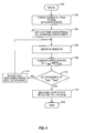
- FIG. 4 is a flow diagram outlining a coarse tuning process according to one embodiment of the present invention.
- the synthesizer 10 includes a fractional-N phase lock loop (PLL) 12 and coarse tuning circuitry 14 .
- the PLL 12 generates a desired frequency for the output signal, F VCO , 16 , of a voltage controlled oscillator (VCO) 18 .
- VCO voltage controlled oscillator
- the output signal F VCO 16 is also provided to divider circuitry 20 to divide the output signal F VCO by a factor N to produce a divided VCO signal F V , which is fed to one of two inputs of a phase detector 22 .
- a reference signal, F REF , 24 is divided by a factor R by divider circuitry 26 to produce a divided reference signal, F R , which is provided to the other input of the phase detector 22 .
- the N and R factors are selected so that the frequencies of the divided reference signal, F R , and the divided VCO signal, F v are equal when the desired output signal, F VCO , 16 , is at a desired frequency.
- the phase detector 22 compares the relative phases of the divided reference signal, F R , and the divided VCO signal, F V , and provides an output relative to the difference in phase to control the VCO 18 .
- the output of the phase detector is preferably provided by a charge pump and filtered by a loop filter 28 to provide a stable voltage for a VCO fine tuning signal, V T , to adjust the desired output frequency F VCO of the VCO 18 based on the difference in phase of the divided reference signal, F R , and the divided VCO signal, F V .
- the dividing factor N is generated by varying the divide value 30 of the divider circuitry 20 in order to provide, on average, a fractional (non-integer) value.
- an integer value, N INT , 34 is combined with a fractional component.
- NUM 32 representing a numerator of the fractional component, is processed by a fractional sequence generator 36 to create a sequence of integer values, which have an average value equal to the desired fraction.
- the fractional sequence generator 36 employs a third order MASH style delta-sigma modulator.
- Each value of the sequence of integer values is summed with the integer value N INT 34 using summing circuitry 38 to create an integer sequence for the divide value 30 .
- the integer sequence will have an average equal to the desired divide value N. Accordingly, the divider circuitry 20 is loaded with a divide value 30 that may vary from one divide cycle to the next in order to achieve the desired fractional division. The result is significant jitter on the divided VCO signal, F V , which reduces the accuracy of traditional techniques for calibrating the VCO 18 .
- the coarse tuning circuitry 14 of the present invention effectively calibrates the frequency range of the VCO 18 for improved fractional-N performance, such as reduced lock time, or improved robustness over environmental variations.
- a divider circuit 40 divides the divided reference signal, F R , by a factor of M to create an average reference signal, F RM .
- Divider circuit 42 divides the divided VCO signal, F V , by a factor of M to create an average VCO signal, F VM .
- the fractional sequence generator 36 employs a third order MASH style delta-sigma modulator
- Tuning logic 44 processes the average reference signal F RM and average VCO signal F VM to provide a VCO control signal VTC CON , which controls calibration of the VCO 18 .
- the tuning logic 44 is a state machine configured to compare the periods of the average VCO signal F VM and average reference signal F RM and provide a pulse for the control signal VTC CON to control a coarse tune counter 46 .
- the output of the coarse tune counter 46 provides select signal VTC SEL to select a capacitance value of the VCO's resonant circuit.
- the tuning logic 44 may generate the VCO select signal VTC SEL directly, for example, as the output of a state machine.
- the VCO fine tuning signal V T is forced to a desired initialization value (voltage or current) under the control of the tuning logic 44 .
- the initialization value, V INIT is coupled to the output of the loop filter 28 to force the VCO fine tuning signal V T to the initialization value, V INIT .
- the switch 48 may take many forms, including a transistor biased to provide a switching function.
- the initialization value, V INIT may be provided using a variety of techniques.
- control logic 50 provides a digital value to a digital-to-analog converter (DAC) 52 , which provides a corresponding analog voltage for the initialization value, V INIT .
- the tuning logic 44 will typically provide a loop filter control signal, LF CON , to cause switch 48 to apply the initialization voltage, V INIT , to the input of the loop filter 28 . Detail on coarse tuning is provided later in the specification.
- the VCO 18 has a tank circuit 54 including parallel inductance 56 (L), fixed or parasitic capacitance 58 (C P ), variable capacitance 60 (C V ) and switched capacitance 62 (C SW ).
- variable capacitance 60 may be a varactor or other continuously variable capacitance.
- the variable capacitance 60 is typically used for fine tuning under the control of the fine tuning signal V T provided by the PLL 12 .
- the switched capacitance 62 is preferably a network of capacitors 64 , 66 , 68 , which can be selectively switched into or out of the VCO tank circuit 54 via switches 70 , 72 , 74 , respectively, for coarse tuning.
- the switches 70 , 72 , 74 can take many forms, including transistors biased to operate as switches.
- the capacitors 64 , 66 , 68 are preferably binary weighted and switched into the VCO tank circuit 54 under the control of the VCO tank capacitance select signal VTC SEL from the coarse tune counter 46 .
- the VCO tank capacitance select signal VTC SEL is a three bit digital signal, where the bits correspond to the respective capacitance values C, 2C, 4C for the capacitors 64 , 66 , 68 , respectively. Accordingly, VTC signal values 000 (binary) through 111 will correlate to capacitance values 0 through 7C for the switched capacitance 62 of the VCO tank circuit 54 .
- the capacitors may be unit weighted, for example to allow an interdigitated layout for better matching, as is well known in the art.
- a translation circuit may be needed between the output of the coarse tune counter 46 and the VCO 18 .
- a shift register constructed to start with its outputs at logical zero (or one) and shift in a series of logical ones (or zeros) in response to each pulse on the control signal VTC CON may be used.
- the operating characteristics for an exemplary VCO 18 having the above-configured VCO tank circuit 54 are shown in FIG. 3. Since the switched capacitance 62 can be configured to have one of eight capacitance values, the VCO 18 will have eight tuning curves corresponding to the respective capacitance values.
- the bottom tuning curve corresponds to having all three capacitors 64 , 66 , 68 switched into the network when the select signal VTC SEL is 111.
- the top tuning curve corresponds to having all three capacitors 64 , 66 , 68 switched out of the network when the select signal VTC SEL is 000.
- V T there are multiple tuning curves capable of providing a selected frequency.
- the voltage of the fine tuning signal, V T should be kept within an acceptable range.
- the Q of the varactor 60 tends to fall off at higher capacitance and lower frequency values.
- the preferred operating range for the VCO 18 corresponds to a fine tuning signal voltage V T between 0.4 and 1.6 volts.
- a coarse tuning process is carried out each time the PLL 12 is enabled.
- the tuning process selects an appropriate capacitance setting for the switched capacitance 62 within a period of time sufficiently short that it does not significantly impact the lock time for the PLL 12 .
- the process operates by comparing the periods of the average VCO signal F VM and the average reference signal F RM and selecting an appropriate capacitance for the switched capacitance 62 to set the frequency of the VCO's output signal F VCO 16 .
- the process repeats for each tuning curve by progressively incrementing or decrementing different capacitance 62 values until an acceptable tuning curve is selected. Further details for the tuning process according to one embodiment of the present invention are provided in association with the flow diagram of FIG. 4.
- the coarse tuning process begins (step 100 ) by forcing the tuning voltage of the VCO fine tuning signal V T to one end of the acceptable range (step 102 ).
- the VCO fine tuning signal V T is forced to 0.4 volts.
- the control logic 50 sends a digital value to the DAC 52 to set the initialization voltage, V INIT , to 0.4 volts.
- the tuning logic 44 will then activate the loop filter control signal LF CON to close switch 48 and apply the initialization voltage, V INIT , to the input of the loop filter 28 .
- Applying a constant voltage to the loop filter 28 which is typically a low pass filter, forces the VCO fine tuning signal V T to 0.4 volts.
- the capacitance of the tank circuit 54 for the VCO 18 is set to select a tuning curve corresponding to a minimum frequency range (step 104 ). Accordingly, the coarse tune counter 46 generates a select signal VTC SEL to switch each of the capacitors 64 , 66 , and 68 into the switched capacitance 62 to set the VCO 18 to operate at the minimum frequency range.
- the select signal VTC SEL is initialized to 111. In alternative embodiments, the VCO 18 may be initialized for the maximum frequency range.
- the switched capacitance 62 is initialized and the VCO fine tuning signal V T is forced to 0.4 volts.
- the tuning logic 44 then compares the frequencies for the average reference signal F RM and the average VCO signal F VM (step 108 ).
- the frequencies of these signals may be determined in a variety of ways.
- the divider 40 receives the divided reference signal F R and provides an output pulse every M cycles to generate the average reference signal F RM .
- the divider 42 receives the divided VCO signal F V and provides an output pulse every M cycles to generate the average VCO signal F VM .
- the tuning logic 44 receives both the average reference signal F RM and the average VCO signal F VM .
- the tuning logic 44 resets each of the divider circuits 40 and 42 with the R ST signal (step 106 ), and then senses whether the first output pulse of the average VCO signal F VM occurs before the first output pulse of the average reference signal F RM , indicating that the frequency of the average VCO signal F VM is higher than that of the average reference signal F RM . Because the frequency of the average reference signal F RM and the frequency of average VCO signal F VM are simply equal to the frequency of the divided reference signal F R and the divided VCO signal F V , respectively, divided by M, this condition also indicates that the frequency of the VCO is higher than the desired operating frequency.
- the tuning logic 44 preferably provides a control signal VTC CON to decrement the coarse tune counter 46 . Decrementing the coarse tune counter 46 results in a VCO select signal VTC SEL decrementing the capacitance value of the switched capacitance 62 to select the next higher tuning curve, which corresponds to the next higher frequency range (step 112 ).
- the periods for the average VCO signal F VM and the average reference signal F RM are again compared, and the switched capacitance 62 is decremented until the frequency of the average VCO signal F VM is greater than the frequency of the average reference signal F RM (step 110 ).
- the tuning logic 44 releases the initialization voltage V INIT from the input of the loop filter 28 via the LP CON signal to allow the PLL 12 to lock (step 114 ) and the process ends (step 116 ).
- the tuning logic 44 will maintain the switched capacitance 62 at the appropriate capacitance via the VCO select signal VTC SEL to ensure that the VCO 18 operates at the appropriate tuning curve.
- the VCO 18 may be initialized for the maximum frequency range wherein the select signal VTC SEL is 000. During coarse tuning, the VCO fine tuning signal V T is forced to 1.6 volts and the switched capacitance 62 is incremented until the frequency of the average VCO signal F VM is less than the frequency of the average reference signal F RM .
- the maximum duration of the coarse tuning process is approximately the period of the average reference frequency, F RM (M*R/F REF ), times the number of capacitance settings for the switched capacitance 62 of the VCO tank circuit 54 .
- F REF the average reference frequency
- an R value of 1 an M value of 64, and eight capacitance settings
- the coarse tuning operation would take at most 20 microseconds before the phase locking in the PLL 12 can begin. Accordingly, the impact of coarse tuning on locking time of the PLL 12 is minimal.
- a binary search algorithm may be employed, in which only one frequency comparison is required for each bit of the VCO control signal VTC CON . In this example, only three comparisons would be needed instead of eight, further reducing the duration of the coarse tuning operation.
- the invention is implemented in a manner minimizing the number of interconnections between the coarse tuning circuitry 14 and the PLL 12 , especially in embodiments where the two circuits are on separate packages or semiconductor die.
- the coarse tune counter 46 and VCO 18 may be placed on a common die, and the coarse tune counter 46 will only require one input to receive the VCO control signal VTC CON to control the value of the switched capacitance 62 of the VCO tank circuit 54 .
- This arrangement reduces the number of pins required on the associated semiconductor packages, or the number of bond pads on the associated die, reducing cost and area.
- ring oscillators can be constructed with coarse and fine tuning control signals provided by switched capacitive loads or switched transistor amplifier stages, and supply voltage or current tuning, respectively. Accordingly, elements, such as gain stages or impedance devices, may be selectively switched into or out of the current or voltage controlled oscillator circuitry to select a tuning curve.
- the counters described herein may be implemented using registers to hold value, or state machines. As such, a counter is deemed to cover and include these configurations.
Landscapes
- Stabilization Of Oscillater, Synchronisation, Frequency Synthesizers (AREA)
Abstract
Description
- The present invention relates in general to fractional-N synthesizers, and, in particular, to a technique to provide coarse tuning of an oscillator in a fractional-N synthesizer.
- Frequency synthesizers are used in many systems, including microprocessors and radio frequency (RF) communication systems. Frequency synthesizers of the phase locked loop (PLL) type contain controlled oscillators (CO) that are typically current controlled oscillators (ICO) or voltage controlled oscillators (VCO). The output of the CO is often used as an injection signal for an RF mixer or in a microprocessor clock system. The frequency synthesizer controls the CO such that its frequency or period is approximately equal to that of a stable frequency reference multiplied by a predetermined ratio. In many applications, there is a need to compensate for process and environmental variations that affect synthesizer performance. The prior art contains many systems that compensate for variations in the CO's frequency tuning range or center frequency by performing a coarse tuning of the tunable elements in the CO. These systems have been developed for integer-N synthesizers where the divided CO signal used for feedback to the phase detector has a steady period when the CO's output frequency is not changing.
- The use of fractional-N synthesizers provides reduced lock times for the synthesizer's phase lock loop (PLL) and improves noise performance, but introduces significant jitter on the divided CO signal. Even with a constant CO output frequency, the divider modulus is constantly changing to provide a desired average fractional modulus over a period of time. The jitter on the divided CO signal significantly reduces the accuracy of existing techniques for calibrating and tuning the CO. Accordingly, there is a need for a technique to reduce the impact of jitter on the divided CO signal and provide accurate calibration or coarse tuning of a CO in a fractional-N synthesizer in a cost-effective and efficient manner.
- The present invention provides an efficient coarse tuning process for fractional-N synthesizers. In general, a reference signal and a divided controllable oscillator (CO) signal from the phase lock loop (PLL) of a synthesizer are each further divided by a common factor M to provide an average reference signal and an average CO signal, respectively. Frequency division by a factor M is an efficient method of adding the durations of M successive periods of the divided CO signal. The period of the average CO signal is approximately equal to M times the average period of the divided CO signal. When the synthesizer is in lock, the average period of the divided CO signal is approximately equal to the period of the reference signal. Hence, the period of the average CO signal is approximately equal to the period of the average reference signal. Averaging the divided CO signal reduces jitter caused by fractional-N division of the CO signal. The frequencies of the average CO signal and the average reference signal are compared and the result is used to select an appropriate tuning curve for operating the CO.
- In one embodiment, the capacitance value of a switched capacitance in the resonant tank or analogous frequency control circuit of the CO is selected based on comparing the frequencies of the average CO and average reference signals. These frequencies may be compared by measuring the periods for the respective signals. Preferably, the process repeats for each tuning curve by progressively incrementing or decrementing the capacitance value of the switched capacitance until an acceptable tuning curve is selected.
- Accordingly, a first divider circuit divides the divided reference signal by a factor of M to create an average reference signal. A second divider circuit divides the divided CO signal by a factor of M to create an average CO signal. Tuning logic processes the average reference signal and average CO signal to provide a CO control signal, which controls calibration of the CO. In the preferred embodiment, the tuning logic is a state machine configured to compare the periods of the average CO signal and average reference signal and provide a pulse for the CO control signal to control a coarse tune counter. The output of the coarse tune counter provides a CO tank capacitance select signal to select a capacitance value of the CO's resonant tank circuit.
- During coarse tuning, the CO fine tuning signal is forced to a desired initialization value under the control of the tuning logic. The tuning logic will typically provide a loop filter control signal to cause a switch to apply the initialization value to the fine tuning signal of the CO. The capacitance of the tank capacitance circuit is incremented or decremented throughout a desired operating range until the average CO signal and average reference signal are substantially the same. At this point, the initialization value is removed from the fine tuning signal and the PLL is allowed to lock in traditional fashion.
- Those skilled in the art will appreciate the scope of the present invention and realize additional aspects thereof after reading the following detailed description of the preferred embodiments in association with the accompanying drawing figures.
- The accompanying drawing figures incorporated in and forming a part of this specification illustrate several aspects of the invention, and together with the description serve to explain the principles of the invention.
- FIG. 1 is a block representation of a fractional-N synthesizer according to one embodiment of the present invention.
- FIG. 2A is a schematic representation of a resonant tank circuit of a voltage controlled oscillator according to one embodiment of the present invention.
- FIG. 2B is an expanded schematic representation of the resonant tank circuit of FIG. 2A.
- FIG. 3 is a graphic representation of the tuning curves for an exemplary voltage controlled oscillator.
- FIG. 4 is a flow diagram outlining a coarse tuning process according to one embodiment of the present invention.
- The embodiments set forth below represent the necessary information to enable those skilled in the art to practice the invention and illustrate the best mode of practicing the invention. Upon reading the following description in light of the accompanying drawing figures, those skilled in the art will understand the concepts of the invention and will recognize applications of these concepts not particularly addressed herein. It should be understood that these concepts and applications fall within the scope of the disclosure and the accompanying claims.
- With reference to FIG. 1, a fractional-
N frequency synthesizer 10 is illustrated according to one embodiment of the present invention. Thesynthesizer 10 includes a fractional-N phase lock loop (PLL) 12 andcoarse tuning circuitry 14. ThePLL 12 generates a desired frequency for the output signal, FVCO, 16, of a voltage controlled oscillator (VCO) 18. In traditional fashion, theoutput signal F VCO 16 is also provided to dividercircuitry 20 to divide the output signal FVCO by a factor N to produce a divided VCO signal FV, which is fed to one of two inputs of aphase detector 22. - A reference signal, F REF, 24, is divided by a factor R by
divider circuitry 26 to produce a divided reference signal, FR, which is provided to the other input of thephase detector 22. The N and R factors are selected so that the frequencies of the divided reference signal, FR, and the divided VCO signal, Fv are equal when the desired output signal, FVCO, 16, is at a desired frequency. Thephase detector 22 compares the relative phases of the divided reference signal, FR, and the divided VCO signal, FV, and provides an output relative to the difference in phase to control theVCO 18. The output of the phase detector is preferably provided by a charge pump and filtered by aloop filter 28 to provide a stable voltage for a VCO fine tuning signal, VT, to adjust the desired output frequency FVCO of theVCO 18 based on the difference in phase of the divided reference signal, FR, and the divided VCO signal, FV. - For the fractional-
N frequency synthesizer 10, the dividing factor N is generated by varying thedivide value 30 of thedivider circuitry 20 in order to provide, on average, a fractional (non-integer) value. To create thedivide value 30, an integer value, NINT, 34, is combined with a fractional component. Traditionally, a number,NUM 32, representing a numerator of the fractional component, is processed by afractional sequence generator 36 to create a sequence of integer values, which have an average value equal to the desired fraction. In one embodiment, thefractional sequence generator 36 employs a third order MASH style delta-sigma modulator. - Each value of the sequence of integer values is summed with the
integer value N INT 34 usingsumming circuitry 38 to create an integer sequence for thedivide value 30. The integer sequence will have an average equal to the desired divide value N. Accordingly, thedivider circuitry 20 is loaded with adivide value 30 that may vary from one divide cycle to the next in order to achieve the desired fractional division. The result is significant jitter on the divided VCO signal, FV, which reduces the accuracy of traditional techniques for calibrating theVCO 18. - The
coarse tuning circuitry 14 of the present invention effectively calibrates the frequency range of theVCO 18 for improved fractional-N performance, such as reduced lock time, or improved robustness over environmental variations. In general, adivider circuit 40 divides the divided reference signal, FR, by a factor of M to create an average reference signal, FRM. Divider circuit 42 divides the divided VCO signal, FV, by a factor of M to create an average VCO signal, FVM. Dividing the divided reference frequency, FR, and the divided VCO frequency, FV, by the factor M effectively averages the divided reference frequency, FR, and the divided VCO frequency, FV, over M periods and significantly reduces the jitter appearing on the divided VCO frequency, FV. In one embodiment, where thefractional sequence generator 36 employs a third order MASH style delta-sigma modulator, sufficient smoothing of the divided VCO frequency, FV, is provided when thedivider circuits -
Tuning logic 44 processes the average reference signal FRM and average VCO signal FVM to provide a VCO control signal VTCCON, which controls calibration of theVCO 18. In the preferred embodiment, the tuninglogic 44 is a state machine configured to compare the periods of the average VCO signal FVM and average reference signal FRM and provide a pulse for the control signal VTCCON to control acoarse tune counter 46. The output of thecoarse tune counter 46 provides select signal VTCSEL to select a capacitance value of the VCO's resonant circuit. Alternatively, the tuninglogic 44 may generate the VCO select signal VTCSEL directly, for example, as the output of a state machine. - During coarse tuning, the VCO fine tuning signal V T is forced to a desired initialization value (voltage or current) under the control of the
tuning logic 44. Using aswitch 48, the initialization value, VINIT, is coupled to the output of theloop filter 28 to force the VCO fine tuning signal VT to the initialization value, VINIT. Theswitch 48 may take many forms, including a transistor biased to provide a switching function. The initialization value, VINIT, may be provided using a variety of techniques. In one embodiment,control logic 50 provides a digital value to a digital-to-analog converter (DAC) 52, which provides a corresponding analog voltage for the initialization value, VINIT. The tuninglogic 44 will typically provide a loop filter control signal, LFCON, to causeswitch 48 to apply the initialization voltage, VINIT, to the input of theloop filter 28. Detail on coarse tuning is provided later in the specification. - With reference to FIG. 2A, the
VCO 18 has atank circuit 54 including parallel inductance 56 (L), fixed or parasitic capacitance 58 (CP), variable capacitance 60 (CV) and switched capacitance 62 (CSW). The resonant frequency of the tank circuits is defined by:
- The
variable capacitance 60 may be a varactor or other continuously variable capacitance. Thevariable capacitance 60 is typically used for fine tuning under the control of the fine tuning signal VT provided by thePLL 12. - As shown in FIG. 2B, the switched
capacitance 62 is preferably a network ofcapacitors VCO tank circuit 54 viaswitches switches capacitors VCO tank circuit 54 under the control of the VCO tank capacitance select signal VTCSEL from thecoarse tune counter 46. The VCO tank capacitance select signal VTCSEL is a three bit digital signal, where the bits correspond to the respective capacitance values C, 2C, 4C for thecapacitors capacitance values 0 through 7C for the switchedcapacitance 62 of theVCO tank circuit 54. Alternatively, the capacitors may be unit weighted, for example to allow an interdigitated layout for better matching, as is well known in the art. In this case, a translation circuit may be needed between the output of thecoarse tune counter 46 and theVCO 18. Those skilled in the art will recognize that a variety of simpler techniques may be used to achieve this same translation. For example, in place of thecoarse tune counter 46, a shift register constructed to start with its outputs at logical zero (or one) and shift in a series of logical ones (or zeros) in response to each pulse on the control signal VTCCON may be used. - The operating characteristics for an
exemplary VCO 18 having the above-configuredVCO tank circuit 54 are shown in FIG. 3. Since the switchedcapacitance 62 can be configured to have one of eight capacitance values, theVCO 18 will have eight tuning curves corresponding to the respective capacitance values. The bottom tuning curve corresponds to having all threecapacitors capacitors VCO 18, the voltage of the fine tuning signal, VT, should be kept within an acceptable range. Typically, the Q of thevaractor 60 tends to fall off at higher capacitance and lower frequency values. For this example, assume the preferred operating range for theVCO 18 corresponds to a fine tuning signal voltage VT between 0.4 and 1.6 volts. - In operation, a coarse tuning process is carried out each time the
PLL 12 is enabled. The tuning process selects an appropriate capacitance setting for the switchedcapacitance 62 within a period of time sufficiently short that it does not significantly impact the lock time for thePLL 12. In general, the process operates by comparing the periods of the average VCO signal FVM and the average reference signal FRM and selecting an appropriate capacitance for the switchedcapacitance 62 to set the frequency of the VCO'soutput signal F VCO 16. Preferably, the process repeats for each tuning curve by progressively incrementing or decrementingdifferent capacitance 62 values until an acceptable tuning curve is selected. Further details for the tuning process according to one embodiment of the present invention are provided in association with the flow diagram of FIG. 4. - The coarse tuning process begins (step 100) by forcing the tuning voltage of the VCO fine tuning signal VT to one end of the acceptable range (step 102). For the illustrated example, the VCO fine tuning signal VT is forced to 0.4 volts. Assume the
control logic 50 sends a digital value to theDAC 52 to set the initialization voltage, VINIT, to 0.4 volts. The tuninglogic 44 will then activate the loop filter control signal LFCON to closeswitch 48 and apply the initialization voltage, VINIT, to the input of theloop filter 28. Applying a constant voltage to theloop filter 28, which is typically a low pass filter, forces the VCO fine tuning signal VT to 0.4 volts. - Next, the capacitance of the
tank circuit 54 for theVCO 18 is set to select a tuning curve corresponding to a minimum frequency range (step 104). Accordingly, thecoarse tune counter 46 generates a select signal VTCSEL to switch each of thecapacitors capacitance 62 to set theVCO 18 to operate at the minimum frequency range. In this example, the select signal VTCSEL is initialized to 111. In alternative embodiments, theVCO 18 may be initialized for the maximum frequency range. - At the start of the coarse tuning operation, the switched
capacitance 62 is initialized and the VCO fine tuning signal VT is forced to 0.4 volts. The tuninglogic 44 then compares the frequencies for the average reference signal FRM and the average VCO signal FVM (step 108). - The frequencies of these signals may be determined in a variety of ways. In the preferred embodiment, the
divider 40 receives the divided reference signal FR and provides an output pulse every M cycles to generate the average reference signal FRM. Similarly, thedivider 42 receives the divided VCO signal FV and provides an output pulse every M cycles to generate the average VCO signal FVM. The tuninglogic 44 receives both the average reference signal FRM and the average VCO signal FVM. Preferably, the tuninglogic 44 resets each of thedivider circuits - With the voltage of the tuning signal at 0.4 volts, the frequency of the output signal F VCO is higher than that desired when the appropriate tuning curve is selected. By comparing the respective periods, if the frequency of the average VCO signal FVM is determined to be less than that of the average reference FRM signal (i.e. the period for FVM is greater than FRM) (step 110), the tuning
logic 44 preferably provides a control signal VTCCON to decrement thecoarse tune counter 46. Decrementing thecoarse tune counter 46 results in a VCO select signal VTCSEL decrementing the capacitance value of the switchedcapacitance 62 to select the next higher tuning curve, which corresponds to the next higher frequency range (step 112). - The periods for the average VCO signal F VM and the average reference signal FRM are again compared, and the switched
capacitance 62 is decremented until the frequency of the average VCO signal FVM is greater than the frequency of the average reference signal FRM (step 110). Once the frequency of the average VCO signal FVM is greater than the frequency of the average reference signal FRM, the tuninglogic 44 releases the initialization voltage VINIT from the input of theloop filter 28 via the LPCON signal to allow thePLL 12 to lock (step 114) and the process ends (step 116). The tuninglogic 44 will maintain the switchedcapacitance 62 at the appropriate capacitance via the VCO select signal VTCSEL to ensure that theVCO 18 operates at the appropriate tuning curve. - Alternatively, the
VCO 18 may be initialized for the maximum frequency range wherein the select signal VTCSEL is 000. During coarse tuning, the VCO fine tuning signal VT is forced to 1.6 volts and the switchedcapacitance 62 is incremented until the frequency of the average VCO signal FVM is less than the frequency of the average reference signal FRM. - The maximum duration of the coarse tuning process is approximately the period of the average reference frequency, F RM (M*R/FREF), times the number of capacitance settings for the switched
capacitance 62 of theVCO tank circuit 54. For a 26 MHz reference frequency FREF, an R value of 1, an M value of 64, and eight capacitance settings, the coarse tuning operation would take at most 20 microseconds before the phase locking in thePLL 12 can begin. Accordingly, the impact of coarse tuning on locking time of thePLL 12 is minimal. Alternatively, a binary search algorithm may be employed, in which only one frequency comparison is required for each bit of the VCO control signal VTCCON. In this example, only three comparisons would be needed instead of eight, further reducing the duration of the coarse tuning operation. - Preferably, the invention is implemented in a manner minimizing the number of interconnections between the
coarse tuning circuitry 14 and thePLL 12, especially in embodiments where the two circuits are on separate packages or semiconductor die. For example, thecoarse tune counter 46 andVCO 18 may be placed on a common die, and thecoarse tune counter 46 will only require one input to receive the VCO control signal VTCCON to control the value of the switchedcapacitance 62 of theVCO tank circuit 54. This arrangement reduces the number of pins required on the associated semiconductor packages, or the number of bond pads on the associated die, reducing cost and area. - It will be recognized that the above discussion applies equally well to other types of oscillators that may be used with fractional-N frequency synthesizers. For example, ring oscillators can be constructed with coarse and fine tuning control signals provided by switched capacitive loads or switched transistor amplifier stages, and supply voltage or current tuning, respectively. Accordingly, elements, such as gain stages or impedance devices, may be selectively switched into or out of the current or voltage controlled oscillator circuitry to select a tuning curve. Further, the counters described herein may be implemented using registers to hold value, or state machines. As such, a counter is deemed to cover and include these configurations.
- Additional detail pertaining to ring oscillators is found in, “An all-digital phase-locked loop with 50-cycle lock time suitable for high-performance microprocessors,” by J. Dunning et al., IEEE Journal of Solid-State Circuits,
Volume 30, Issue 4, April 1995, pages 412-422. - Those skilled in the art will recognize improvements and modifications to the preferred embodiments of the present invention. All such improvements and modifications are considered within the scope of the concepts disclosed herein and the claims that follow.
Claims (40)
Priority Applications (1)
| Application Number | Priority Date | Filing Date | Title |
|---|---|---|---|
| US10/127,289 US6710664B2 (en) | 2002-04-22 | 2002-04-22 | Coarse tuning for fractional-N synthesizers |
Applications Claiming Priority (1)
| Application Number | Priority Date | Filing Date | Title |
|---|---|---|---|
| US10/127,289 US6710664B2 (en) | 2002-04-22 | 2002-04-22 | Coarse tuning for fractional-N synthesizers |
Publications (2)
| Publication Number | Publication Date |
|---|---|
| US20030197564A1 true US20030197564A1 (en) | 2003-10-23 |
| US6710664B2 US6710664B2 (en) | 2004-03-23 |
Family
ID=29215227
Family Applications (1)
| Application Number | Title | Priority Date | Filing Date |
|---|---|---|---|
| US10/127,289 Expired - Lifetime US6710664B2 (en) | 2002-04-22 | 2002-04-22 | Coarse tuning for fractional-N synthesizers |
Country Status (1)
| Country | Link |
|---|---|
| US (1) | US6710664B2 (en) |
Cited By (30)
| Publication number | Priority date | Publication date | Assignee | Title |
|---|---|---|---|---|
| US20030224748A1 (en) * | 2002-05-31 | 2003-12-04 | Broadcom Corporation | Double-conversion television tuner using a delta-sigma fractional-N PLL |
| US6809597B2 (en) * | 2002-03-28 | 2004-10-26 | Nec Electronics Corporation | Phase comparison method, phase comparison circuit, and phase locked loop (PLL) type circuit |
| EP1551102A1 (en) * | 2003-12-29 | 2005-07-06 | STMicroelectronics S.r.l. | Device for calibrating the frequency of an oscillator, phase looked loop circuit comprising said calibration device and related frequency calibration method. |
| US20050258906A1 (en) * | 2004-05-24 | 2005-11-24 | Chih-Chin Su | Self-calibrating, fast-locking frequency synthesizer |
| US20060094374A1 (en) * | 2003-03-05 | 2006-05-04 | Olip John A P | Frequency synthesizer and synthesis method for generating a multiband local oscillator signal |
| US20060226916A1 (en) * | 2005-04-11 | 2006-10-12 | Octavian Florescu | PLL lock management system |
| FR2896641A1 (en) * | 2006-01-24 | 2007-07-27 | St Microelectronics Sa | Voltage controller oscillator calibrating method for frequency synthesizer, involves determining impedance value for modifying output frequency of oscillator so as to correspond to reference frequency, and connecting impedance to oscillator |
| US7412213B1 (en) | 2001-07-23 | 2008-08-12 | Sequoia Communications | Envelope limiting for polar modulators |
| US7479815B1 (en) | 2005-03-01 | 2009-01-20 | Sequoia Communications | PLL with dual edge sensitivity |
| US7489916B1 (en) | 2002-06-04 | 2009-02-10 | Sequoia Communications | Direct down-conversion mixer architecture |
| US7496338B1 (en) | 2003-12-29 | 2009-02-24 | Sequoia Communications | Multi-segment gain control system |
| US7522005B1 (en) | 2006-07-28 | 2009-04-21 | Sequoia Communications | KFM frequency tracking system using an analog correlator |
| US7522017B1 (en) | 2004-04-21 | 2009-04-21 | Sequoia Communications | High-Q integrated RF filters |
| US7548122B1 (en) | 2005-03-01 | 2009-06-16 | Sequoia Communications | PLL with switched parameters |
| US7587179B1 (en) | 2001-10-04 | 2009-09-08 | Sequoia Communications | Direct synthesis transmitter |
| US7595626B1 (en) | 2005-05-05 | 2009-09-29 | Sequoia Communications | System for matched and isolated references |
| US7609118B1 (en) | 2003-12-29 | 2009-10-27 | Sequoia Communications | Phase-locked loop calibration system |
| US7672648B1 (en) | 2004-06-26 | 2010-03-02 | Quintics Holdings | System for linear amplitude modulation |
| US7675379B1 (en) | 2005-03-05 | 2010-03-09 | Quintics Holdings | Linear wideband phase modulation system |
| US7679468B1 (en) | 2006-07-28 | 2010-03-16 | Quintic Holdings | KFM frequency tracking system using a digital correlator |
| US20100213984A1 (en) * | 2009-02-24 | 2010-08-26 | Kwangwoon University Industry-Academic Collaboration Foundation | Automatic frequency calibration apparatus and method for a phase-locked loop based frequency synthesizer |
| US7894545B1 (en) | 2006-08-14 | 2011-02-22 | Quintic Holdings | Time alignment of polar transmitter |
| US20110057696A1 (en) * | 2009-09-04 | 2011-03-10 | Mstar Semiconductor, Inc. | Frequency Calibration Apparatus of Phase Locked Loop and Method Thereof |
| US7920033B1 (en) | 2006-09-28 | 2011-04-05 | Groe John B | Systems and methods for frequency modulation adjustment |
| US7974374B2 (en) | 2006-05-16 | 2011-07-05 | Quintic Holdings | Multi-mode VCO for direct FM systems |
| US20130278303A1 (en) * | 2012-04-20 | 2013-10-24 | Taiwan Semiconductor Manufacturing Company, Ltd. | Auto frequency calibration for a phase locked loop and method of use |
| US8912857B2 (en) | 2008-04-18 | 2014-12-16 | Freescale Semiconductor, Inc. | PLL system and method for controlling a gain of a VCO circuit |
| US20160079988A1 (en) * | 2014-09-12 | 2016-03-17 | Seiko Epson Corporation | Fractional n-pll circuit, oscillator, electronic device, and moving object |
| US9503017B1 (en) | 2009-09-29 | 2016-11-22 | Qorvo Us, Inc. | Infrastructure-grade integrated voltage controlled oscillator (VCO) with linear tuning characteristics and low phase noise |
| US20170324418A1 (en) * | 2016-05-06 | 2017-11-09 | Raydium Semiconductor Corporation | Frequency Synthesizing Device and Automatic Calibration Method Thereof |
Families Citing this family (30)
| Publication number | Priority date | Publication date | Assignee | Title |
|---|---|---|---|---|
| US7027796B1 (en) | 2001-06-22 | 2006-04-11 | Rfmd Wpan, Inc. | Method and apparatus for automatic fast locking power conserving synthesizer |
| US7019595B1 (en) * | 2002-10-25 | 2006-03-28 | Ralink Technology, Inc. | Frequency synthesizer with automatic tuning control to increase tuning range |
| US6831506B1 (en) | 2003-09-17 | 2004-12-14 | Rf Micro Devices, Inc. | Reconfigurable filter architecture |
| KR100532476B1 (en) * | 2003-10-18 | 2005-12-01 | 삼성전자주식회사 | Frequency synthesizer using a wide-band voltage controlled oscillator and fast adaptive frequency calibration technique |
| DE10354522B4 (en) * | 2003-11-14 | 2006-10-26 | Atmel Germany Gmbh | Method and circuit for generating a control voltage for a voltage-controlled oscillator |
| US6980039B1 (en) | 2004-03-03 | 2005-12-27 | Rf Micro Devices, Inc. | DC-DC converter with noise spreading to meet spectral mask requirements |
| US6891414B1 (en) | 2004-03-05 | 2005-05-10 | Rf Micro Devices, Inc. | Digital calibration for capacitor voltage non-linearity |
| US7023282B1 (en) | 2004-05-11 | 2006-04-04 | Rf Micro Devices, Inc. | Coarse tuning for fractional-N synthesizers having reduced period comparison error |
| US7064591B1 (en) | 2004-05-11 | 2006-06-20 | Rf Micro Devices, Inc. | Coarse tuning for fractional-N synthesizers |
| US7151363B1 (en) | 2004-06-08 | 2006-12-19 | Rf Micro Devices, Inc. | High PSRR, fast settle time voltage regulator |
| US7336134B1 (en) | 2004-06-25 | 2008-02-26 | Rf Micro Devices, Inc. | Digitally controlled oscillator |
| US7098754B2 (en) * | 2005-01-31 | 2006-08-29 | Rf Micro Devices, Inc. | Fractional-N offset phase locked loop |
| US7474878B1 (en) | 2005-03-02 | 2009-01-06 | Rf Micro Devices, Inc. | Closed loop polar modulation system with open loop option at low power levels |
| US7279988B1 (en) | 2005-03-17 | 2007-10-09 | Rf Micro Devices, Inc. | Digital frequency locked loop and phase locked loop frequency synthesizer |
| US7932784B1 (en) | 2005-03-17 | 2011-04-26 | Rf Micro Devices, Inc. | Frequency and phase locked loop synthesizer |
| WO2006125473A1 (en) * | 2005-05-26 | 2006-11-30 | Freescale Semiconductor, Inc | Frequency generation in a wireless communication unit |
| US8224265B1 (en) * | 2005-06-13 | 2012-07-17 | Rf Micro Devices, Inc. | Method for optimizing AM/AM and AM/PM predistortion in a mobile terminal |
| TWI296464B (en) * | 2005-06-20 | 2008-05-01 | Airoha Tech Corp | Phase lock loop and operating method thereof |
| KR100682279B1 (en) * | 2005-07-14 | 2007-02-15 | (주)에프씨아이 | Adaptive frequency regulator of frequency synthesizer |
| US7482885B2 (en) * | 2005-12-29 | 2009-01-27 | Orca Systems, Inc. | Method of frequency synthesis for fast switching |
| US7519349B2 (en) * | 2006-02-17 | 2009-04-14 | Orca Systems, Inc. | Transceiver development in VHF/UHF/GSM/GPS/bluetooth/cordless telephones |
| KR100847687B1 (en) * | 2006-10-20 | 2008-07-23 | (주)에프씨아이 | Frequency Synthesizer and Frequency Control Method |
| KR101316890B1 (en) * | 2007-11-08 | 2013-10-11 | 삼성전자주식회사 | Frequency calibration apparatus and method in frequency synthesizer |
| KR100925156B1 (en) | 2007-11-26 | 2009-11-05 | (주)카이로넷 | Adaptive frequency correction device and wideband frequency synthesizer including same |
| US7898343B1 (en) | 2007-12-21 | 2011-03-01 | Rf Micro Devices, Inc. | Frequency-locked loop calibration of a phase-locked loop gain |
| US7956696B2 (en) * | 2008-09-19 | 2011-06-07 | Altera Corporation | Techniques for generating fractional clock signals |
| WO2010141330A1 (en) | 2009-06-02 | 2010-12-09 | Boehringer Ingelheim International Gmbh | DERIVATIVES OF 6,7-DIHYDRO-5H-IMIDAZO[1,2-a]IMIDAZOLE-3-CARBOXYLIC ACID AMIDES |
| TWI362835B (en) * | 2010-03-11 | 2012-04-21 | Ind Tech Res Inst | Automatic frequency calibration circuit and method for frequency synthesizer |
| JP5659104B2 (en) * | 2011-08-24 | 2015-01-28 | 株式会社東芝 | Frequency adjustment circuit, phase synchronization circuit, communication device, and storage device |
| US8618840B1 (en) * | 2012-07-11 | 2013-12-31 | Fujitsu Limited | Frequency synthesizer tuning |
Citations (6)
| Publication number | Priority date | Publication date | Assignee | Title |
|---|---|---|---|---|
| US3538450A (en) * | 1968-11-04 | 1970-11-03 | Collins Radio Co | Phase locked loop with digital capacitor and varactor tuned oscillator |
| US4875046A (en) * | 1986-07-11 | 1989-10-17 | Brooktree Corporation | Centroiding algorithm for networks used in A/D and D/A converters |
| US5117206A (en) * | 1989-12-05 | 1992-05-26 | Seiko Epson Corporation | Variable capacitance integrated circuit usable in temperature compensated oscillators |
| US5235335A (en) * | 1992-06-02 | 1993-08-10 | Texas Instruments Incorporated | Circuit and method for tuning capacitor arrays |
| US5493715A (en) * | 1994-08-01 | 1996-02-20 | Motorola, Inc. | Multi-range voltage controlled resonant circuit |
| US5973633A (en) * | 1996-12-20 | 1999-10-26 | Texas Instruments Incorporated | Weighted capacitor array with selective grouping to form array elements |
Family Cites Families (2)
| Publication number | Priority date | Publication date | Assignee | Title |
|---|---|---|---|---|
| JPH0677820A (en) * | 1992-08-27 | 1994-03-18 | Fujitsu Ltd | Pll circuit and fault detection method for pll circuit |
| JPH0799446A (en) * | 1993-03-02 | 1995-04-11 | Mitsubishi Electric Corp | PLL circuit |
-
2002
- 2002-04-22 US US10/127,289 patent/US6710664B2/en not_active Expired - Lifetime
Patent Citations (6)
| Publication number | Priority date | Publication date | Assignee | Title |
|---|---|---|---|---|
| US3538450A (en) * | 1968-11-04 | 1970-11-03 | Collins Radio Co | Phase locked loop with digital capacitor and varactor tuned oscillator |
| US4875046A (en) * | 1986-07-11 | 1989-10-17 | Brooktree Corporation | Centroiding algorithm for networks used in A/D and D/A converters |
| US5117206A (en) * | 1989-12-05 | 1992-05-26 | Seiko Epson Corporation | Variable capacitance integrated circuit usable in temperature compensated oscillators |
| US5235335A (en) * | 1992-06-02 | 1993-08-10 | Texas Instruments Incorporated | Circuit and method for tuning capacitor arrays |
| US5493715A (en) * | 1994-08-01 | 1996-02-20 | Motorola, Inc. | Multi-range voltage controlled resonant circuit |
| US5973633A (en) * | 1996-12-20 | 1999-10-26 | Texas Instruments Incorporated | Weighted capacitor array with selective grouping to form array elements |
Cited By (47)
| Publication number | Priority date | Publication date | Assignee | Title |
|---|---|---|---|---|
| US7412213B1 (en) | 2001-07-23 | 2008-08-12 | Sequoia Communications | Envelope limiting for polar modulators |
| US7587179B1 (en) | 2001-10-04 | 2009-09-08 | Sequoia Communications | Direct synthesis transmitter |
| US6809597B2 (en) * | 2002-03-28 | 2004-10-26 | Nec Electronics Corporation | Phase comparison method, phase comparison circuit, and phase locked loop (PLL) type circuit |
| US20030224748A1 (en) * | 2002-05-31 | 2003-12-04 | Broadcom Corporation | Double-conversion television tuner using a delta-sigma fractional-N PLL |
| US7072633B2 (en) * | 2002-05-31 | 2006-07-04 | Broadcom Corporation | Double-conversion television tuner using a Delta-Sigma Fractional-N PLL |
| US7489916B1 (en) | 2002-06-04 | 2009-02-10 | Sequoia Communications | Direct down-conversion mixer architecture |
| US7515931B2 (en) * | 2003-03-05 | 2009-04-07 | Cisco Technology, Inc. | Frequency synthesizer and synthesis method for generating a multiband local oscillator signal |
| US20060094374A1 (en) * | 2003-03-05 | 2006-05-04 | Olip John A P | Frequency synthesizer and synthesis method for generating a multiband local oscillator signal |
| US7609118B1 (en) | 2003-12-29 | 2009-10-27 | Sequoia Communications | Phase-locked loop calibration system |
| US7129793B2 (en) | 2003-12-29 | 2006-10-31 | Stmicroelectronics S.R.L. | Device for calibrating the frequency of an oscillator, phase looked loop circuit comprising said calibration device and related frequency calibration method |
| US20050156677A1 (en) * | 2003-12-29 | 2005-07-21 | Stmicroelectronics S.R.I. | Device for calibrating the frequency of an oscillator, phase looked loop circuit comprising said calibration device and related frequency calibration method |
| US7496338B1 (en) | 2003-12-29 | 2009-02-24 | Sequoia Communications | Multi-segment gain control system |
| EP1551102A1 (en) * | 2003-12-29 | 2005-07-06 | STMicroelectronics S.r.l. | Device for calibrating the frequency of an oscillator, phase looked loop circuit comprising said calibration device and related frequency calibration method. |
| US7522017B1 (en) | 2004-04-21 | 2009-04-21 | Sequoia Communications | High-Q integrated RF filters |
| US7042253B2 (en) * | 2004-05-24 | 2006-05-09 | Industrial Technology Research Institute (Itri) | Self-calibrating, fast-locking frequency synthesizer |
| US20050258906A1 (en) * | 2004-05-24 | 2005-11-24 | Chih-Chin Su | Self-calibrating, fast-locking frequency synthesizer |
| US7672648B1 (en) | 2004-06-26 | 2010-03-02 | Quintics Holdings | System for linear amplitude modulation |
| US7479815B1 (en) | 2005-03-01 | 2009-01-20 | Sequoia Communications | PLL with dual edge sensitivity |
| US7548122B1 (en) | 2005-03-01 | 2009-06-16 | Sequoia Communications | PLL with switched parameters |
| US7675379B1 (en) | 2005-03-05 | 2010-03-09 | Quintics Holdings | Linear wideband phase modulation system |
| US7323944B2 (en) | 2005-04-11 | 2008-01-29 | Qualcomm Incorporated | PLL lock management system |
| WO2006110907A3 (en) * | 2005-04-11 | 2007-03-08 | Qualcomm Inc | Pll lock management system |
| US20060226916A1 (en) * | 2005-04-11 | 2006-10-12 | Octavian Florescu | PLL lock management system |
| US7595626B1 (en) | 2005-05-05 | 2009-09-29 | Sequoia Communications | System for matched and isolated references |
| FR2896641A1 (en) * | 2006-01-24 | 2007-07-27 | St Microelectronics Sa | Voltage controller oscillator calibrating method for frequency synthesizer, involves determining impedance value for modifying output frequency of oscillator so as to correspond to reference frequency, and connecting impedance to oscillator |
| US20070188245A1 (en) * | 2006-01-24 | 2007-08-16 | Stmicroelectronics Sa | Calibrating an oscillator and corresponding calibration device |
| US7821345B2 (en) | 2006-01-24 | 2010-10-26 | Stmicroelectronics Sa | Calibrating an oscillator and corresponding calibration device |
| US7974374B2 (en) | 2006-05-16 | 2011-07-05 | Quintic Holdings | Multi-mode VCO for direct FM systems |
| US7679468B1 (en) | 2006-07-28 | 2010-03-16 | Quintic Holdings | KFM frequency tracking system using a digital correlator |
| US7522005B1 (en) | 2006-07-28 | 2009-04-21 | Sequoia Communications | KFM frequency tracking system using an analog correlator |
| US7894545B1 (en) | 2006-08-14 | 2011-02-22 | Quintic Holdings | Time alignment of polar transmitter |
| US7920033B1 (en) | 2006-09-28 | 2011-04-05 | Groe John B | Systems and methods for frequency modulation adjustment |
| US8912857B2 (en) | 2008-04-18 | 2014-12-16 | Freescale Semiconductor, Inc. | PLL system and method for controlling a gain of a VCO circuit |
| US20100213984A1 (en) * | 2009-02-24 | 2010-08-26 | Kwangwoon University Industry-Academic Collaboration Foundation | Automatic frequency calibration apparatus and method for a phase-locked loop based frequency synthesizer |
| US7982552B2 (en) * | 2009-02-24 | 2011-07-19 | Kwangwoon University Industry-Academic Collaboration Foundation | Automatic frequency calibration apparatus and method for a phase-locked loop based frequency synthesizer |
| US9479184B2 (en) * | 2009-09-04 | 2016-10-25 | Mstar Semiconductor, Inc. | Frequency calibration apparatus of phase locked loop and method thereof |
| US20110057696A1 (en) * | 2009-09-04 | 2011-03-10 | Mstar Semiconductor, Inc. | Frequency Calibration Apparatus of Phase Locked Loop and Method Thereof |
| US9503017B1 (en) | 2009-09-29 | 2016-11-22 | Qorvo Us, Inc. | Infrastructure-grade integrated voltage controlled oscillator (VCO) with linear tuning characteristics and low phase noise |
| US20130278303A1 (en) * | 2012-04-20 | 2013-10-24 | Taiwan Semiconductor Manufacturing Company, Ltd. | Auto frequency calibration for a phase locked loop and method of use |
| US8953730B2 (en) * | 2012-04-20 | 2015-02-10 | Taiwan Semiconductor Manufacturing Company, Ltd. | Auto frequency calibration for a phase locked loop and method of use |
| US20150130518A1 (en) * | 2012-04-20 | 2015-05-14 | Taiwan Semiconductor Manufacturing Company, Ltd. | Auto frequency calibration for a phase locked loop and method of use |
| US9490819B2 (en) * | 2012-04-20 | 2016-11-08 | Taiwan Semiconductor Manufacturing Company, Ltd. | Auto frequency calibration for a phase locked loop and method of use |
| US9838024B2 (en) | 2012-04-20 | 2017-12-05 | Taiwan Semiconductor Manufacturing Company, Ltd. | Auto frequency calibration method |
| US20160079988A1 (en) * | 2014-09-12 | 2016-03-17 | Seiko Epson Corporation | Fractional n-pll circuit, oscillator, electronic device, and moving object |
| US9490820B2 (en) * | 2014-09-12 | 2016-11-08 | Seiko Epson Corporation | Fractional N-PLL circuit, oscillator, electronic device, and moving object |
| US20170324418A1 (en) * | 2016-05-06 | 2017-11-09 | Raydium Semiconductor Corporation | Frequency Synthesizing Device and Automatic Calibration Method Thereof |
| US10218367B2 (en) * | 2016-05-06 | 2019-02-26 | Raydium Semiconductor Corporation | Frequency synthesizing device and automatic calibration method thereof |
Also Published As
| Publication number | Publication date |
|---|---|
| US6710664B2 (en) | 2004-03-23 |
Similar Documents
| Publication | Publication Date | Title |
|---|---|---|
| US6710664B2 (en) | Coarse tuning for fractional-N synthesizers | |
| US7064591B1 (en) | Coarse tuning for fractional-N synthesizers | |
| US6838951B1 (en) | Frequency synthesizer having VCO bias current compensation | |
| US6229399B1 (en) | Multiple frequency band synthesizer using a single voltage control oscillator | |
| US9042854B2 (en) | Apparatus and methods for tuning a voltage controlled oscillator | |
| KR100847687B1 (en) | Frequency Synthesizer and Frequency Control Method | |
| US6744323B1 (en) | Method for phase locking in a phase lock loop | |
| CN100574092C (en) | Voltage Controlled Digital Analog Oscillator and Frequency Synthesizer Using the Oscillator | |
| US7019569B2 (en) | Method of implementing multi-transfer curve phase lock loop | |
| US7443254B2 (en) | Relaxation oscillator with propagation delay compensation for improving the linearity and maximum frequency | |
| US20070247200A1 (en) | Frequency Independent Control | |
| US20090128241A1 (en) | Analogue self-calibration method and apparatus for low noise, fast and wide-locking range phase locked loop | |
| KR100880422B1 (en) | Fractional Frequency Synthesizer with Fractional Compensation Method | |
| US7327820B2 (en) | Method and apparatus for reducing quantization noise in fractional-N frequency synthesizers | |
| US7023283B2 (en) | Wide lock range phase locked loop and method of operation | |
| US7023282B1 (en) | Coarse tuning for fractional-N synthesizers having reduced period comparison error | |
| CN101622788A (en) | PLL frequency synthesizer | |
| US6597250B2 (en) | Low-noise and rapid response frequency synthesizer, and corresponding frequency synthesizing method | |
| US10340902B1 (en) | Multiplying delay locked loops with compensation for realignment error | |
| KR0149126B1 (en) | Hybrid Frequency Synthesizer | |
| JP2004080624A (en) | Frequency synthesizer | |
| JP2001060870A (en) | Frequency synthesizer device, frequency generation method, and mobile wireless device | |
| JP3110318B2 (en) | Phase locked loop / frequency synthesizer | |
| US20050266816A1 (en) | PLL synthesizer | |
| JPH11239056A (en) | Pll oscillation circuit |
Legal Events
| Date | Code | Title | Description |
|---|---|---|---|
| AS | Assignment |
Owner name: RF MICRO DEVICES, INC., NORTH CAROLINA Free format text: ASSIGNMENT OF ASSIGNORS INTEREST;ASSIGNORS:HUMPHREYS, SCOTT ROBERT;NIERI, RALPH CHRISTOPHER;REEL/FRAME:012826/0001 Effective date: 20020419 |
|
| STCF | Information on status: patent grant |
Free format text: PATENTED CASE |
|
| FPAY | Fee payment |
Year of fee payment: 4 |
|
| FPAY | Fee payment |
Year of fee payment: 8 |
|
| AS | Assignment |
Owner name: BANK OF AMERICA, N.A., AS ADMINISTRATIVE AGENT, TE Free format text: NOTICE OF GRANT OF SECURITY INTEREST IN PATENTS;ASSIGNOR:RF MICRO DEVICES, INC.;REEL/FRAME:030045/0831 Effective date: 20130319 |
|
| AS | Assignment |
Owner name: RF MICRO DEVICES, INC., NORTH CAROLINA Free format text: TERMINATION AND RELEASE OF SECURITY INTEREST IN PATENTS (RECORDED 3/19/13 AT REEL/FRAME 030045/0831);ASSIGNOR:BANK OF AMERICA, N.A., AS ADMINISTRATIVE AGENT;REEL/FRAME:035334/0363 Effective date: 20150326 |
|
| FPAY | Fee payment |
Year of fee payment: 12 |
|
| AS | Assignment |
Owner name: QORVO US, INC., NORTH CAROLINA Free format text: MERGER;ASSIGNOR:RF MICRO DEVICES, INC.;REEL/FRAME:039196/0941 Effective date: 20160330 |