EP0331418A2 - EPROM-Programmierungselemente - Google Patents
EPROM-Programmierungselemente Download PDFInfo
- Publication number
- EP0331418A2 EP0331418A2 EP89301957A EP89301957A EP0331418A2 EP 0331418 A2 EP0331418 A2 EP 0331418A2 EP 89301957 A EP89301957 A EP 89301957A EP 89301957 A EP89301957 A EP 89301957A EP 0331418 A2 EP0331418 A2 EP 0331418A2
- Authority
- EP
- European Patent Office
- Prior art keywords
- layer
- gate
- oxide
- polysilicon
- source
- Prior art date
- Legal status (The legal status is an assumption and is not a legal conclusion. Google has not performed a legal analysis and makes no representation as to the accuracy of the status listed.)
- Ceased
Links
Images


Classifications
-
- H10W20/069—
-
- H—ELECTRICITY
- H10—SEMICONDUCTOR DEVICES; ELECTRIC SOLID-STATE DEVICES NOT OTHERWISE PROVIDED FOR
- H10D—INORGANIC ELECTRIC SEMICONDUCTOR DEVICES
- H10D30/00—Field-effect transistors [FET]
- H10D30/60—Insulated-gate field-effect transistors [IGFET]
- H10D30/68—Floating-gate IGFETs
- H10D30/681—Floating-gate IGFETs having only two programming levels
- H10D30/684—Floating-gate IGFETs having only two programming levels programmed by hot carrier injection
- H10D30/686—Floating-gate IGFETs having only two programming levels programmed by hot carrier injection using hot carriers produced by avalanche breakdown of PN junctions, e.g. floating gate avalanche injection MOS [FAMOS]
-
- H—ELECTRICITY
- H10—SEMICONDUCTOR DEVICES; ELECTRIC SOLID-STATE DEVICES NOT OTHERWISE PROVIDED FOR
- H10D—INORGANIC ELECTRIC SEMICONDUCTOR DEVICES
- H10D64/00—Electrodes of devices having potential barriers
- H10D64/01—Manufacture or treatment
- H10D64/031—Manufacture or treatment of data-storage electrodes
- H10D64/035—Manufacture or treatment of data-storage electrodes comprising conductor-insulator-conductor-insulator-semiconductor structures
-
- H10W10/014—
-
- H10W10/17—
Definitions
- the present invention relates to EPROM programming elements, and, more particularly, to a new device structure and process for preparing such elements, resulting in a completely self-aligned structure.
- CMOS complementary MOS
- the depth of focus of the lithography step per becomes smaller.
- the different heights of different features generate a depth of field problem.
- the spacing of contacts to the polysilicon gate and to the field oxide becomes critical at smaller dimensions. It will be appreciated that due to the use of separate alignment steps, the margin of error in aligning the contact can, if not adequate, result in either (a) etching through the field oxide, with consequent shorting of the silicon substrate to the diffusion source or drain region by the contact, or (b) contacting the polysilicon gate, with consequent shorting of the gate to the source or drain contact.
- Such misalignments are accommodated by allowing a substantial space between source, drain and gate and between source, drain and field edge. As a result, high packing density is sacrificed.
- Another requirement of the present processing scheme is that the gate contact is made to an interconnect which extends at right angle to the source-gate-drain line. Such a contact requires considerably more area than a contact directly down to the gate. However, the use of separate alignments dictate the present processing scheme, in order to avoid potential misalignment problems.
- EPROM erasable programmable read only memory
- EPROM elements which are formed by a process which avoids most, if not all, the problems associated with prior art processes.
- a new process is disclosed which is intended to supplant the LOCOS process, for fabricating EPROM elements.
- the process employs planarization processes and total self-alignment to avoid most, if not all, the disadvantages associated with the prior art process. As a result, high packing densities may be achieved.
- Planarization avoids the depth of field problem. Self-alignment easily permits various components of the devices to be interconnected in any manner selected by the engineer, without the misalignment area penalties discussed earlier.
- the disclosed process permits the use of plugs of polysilicon, the tops of which can be contacted to reduce gate contact area requirements. Feature distances of 0.5 ⁇ m and less may be achieved.
- Polysilicon plug contacts through slots in the multi-structure layer permit vertical contact to be made to the various elements.
- the disclosed EPROM element comprises a MOS transistor comprising source and drain regions contacted by source and drain contacts, respectively, separated by a gate region formed on a substrate and is characterized by the gate region comprising two separate gates, a floating gate and a control gate, capacitively coupled together.
- the floating gate is formed on a gate oxide over the substrate and the gates are separated from each other and from the source and drain contacts by a dielectric.
- the process also enables efficient coupling of the floating gate to the control gate by employing "peripheral overlap" of the electrodes.
- the structure enables the control gate to be efficiently decoupled from the source and drain areas by employing a thick intervening dielectric between the areas.
- the disclosed EPROM element has two threshold voltages, one related to the operation of a "normal” MOS transistor and the other related to a “programmed” threshold, following programming of the transistor.
- the voltage on the floating gate is about the same as that of the drain, with the source at ground potential.
- the control gate is made more positive with respect to the drain. This control gate couples to the floating gate, raising its potential. This in turn injects electrons into the gate oxide under the float ing gate, thereby lowering the threshold of the device.
- Sensing the threshold voltage of the device permits a determination to be made whether the device is programmed. UV radiation erases the programming and restores the threshold voltage of the device to its pre-programmed level.
- the disclosed process requires fewer steps than the conventional LOCOS process and provides an EPROM element having both a higher coupling between electrodes and a smaller size.
- the process of the invention in its preferred form, is totally non-LOCOS. However, it will be appreciated by those skilled in the art that portions of the process may be incorporated in the present LOCOS process to realize the benefits disclosed herein. Further, while the process of the invention is directed specifically to employing silicon as the semiconductor, it will be clear to those skilled in the art that the teachings of the invention may be extended to other semiconductors, with suitable modifications in etch-stop layers and the like.
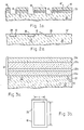
- the process of the invention begins with the formation of an isolation trench 10 surrounding the area in which a device (here, an MOS transistor 14, seen in Fig. 11a), is to be fabricated in a P-well region 12 in a semiconductor substrate 16.
- a device here, an MOS transistor 14, seen in Fig. 11a
- LOCOS oxide could be used, which would permit omission of oxide layer 28a, discussed below.
- transistors 14 comprise source 18 and drain 20 elements, with a gate area 22 therebetween to regulate the extent of a connector 24 therebetween (seen in FIG. 10a).
- the formation of P-wells is known, and hence does not form a part of this invention.
- a plurality of trenches 10 surrounding well regions 12 in a semiconductor substrate 16 are etched through a resist mask 23 formed on top of a nitride mask 25 formed on the surface 16′ of the substrate.
- the resist 23 and the nitride 25 are then stripped and the trenches 10 are filled with an oxide 26, as shown in FIG. 2a.
- the etching of the trench is done employing well-known processes, such as an RIE (reactive ion etch) process followed by suitable wet silicon damage removal etches.
- the oxide 26 used to fill the trenches 10 may be a low temperature oxide or a preferred 750°C TEOS ( tetra -ethyl ortho silicate).
- the oxide is etched back to be planar with the surface 16′ of the silicon substrate 16.
- the planarizing is done by a combination of chemical and reactive ion etching processes commonly used in the art for oxide planarization.
- the isolation trench 10 is created by etching a four-walled trench to outline an active region of the appropriate length (X) and width (Y).
- the trench 10 has a rectangular configuration, when viewed in top plan view (FIG. 3b), defining an active area (X x Y) of about 5 ⁇ m by 2 ⁇ m (for 1 ⁇ m design rules).
- the isolation trench is typically about 0.5 to 1 ⁇ m wide and about 0.4 to 0.6 ⁇ m deep.
- the size is governed by lithography alignment constraints and filling of the trenches by subsequently deposited oxide.
- This multi-layer structure includes a buried stop-etch layer, essential in the practice of the invention.
- a field oxide 28a having a thickness of about 2,500 ⁇ ⁇ 5%, is formed on the surface of the substrate 16.
- the thickness of the field oxide 28a can be targeted consistent with the field threshold voltage required and subsequent implant energy available for forming N ⁇ connectors, described below.
- the formation of the field oxide 28a in itself is not novel, and is formed by a conventional deposition process to the required thicknesses.
- the thickness selected depends upon the implant energy needed to implant therethrough versus the polysilicon left to block the implant, as discussed below in connection with FIG. 10a.
- the field oxide 28a should be as thin as possible consistent with the required field inversion voltages. Also importantly, the thickness of this layer 28a should be substantially uniform across the surface of the wafer, in order to best realize the benefits of the invention.
- the field oxide comprises silicon dioxide.
- the field oxide layer 28a doubles as a decoupling layer between the control gate electrode 58 (see FIG. 12a and the discussion associated therewith) and the extensions to the source and drain junctions (18′ and 20′) formed by the connector implants (delineated 24 in FIG. 12a).
- the floating gate 40g shown in FIG. 9a and subsequent Figures
- the field oxide layer 28a therefore serves a dual purpose of a conventional field oxide in the non-EPROM circuitry and as a decoupling dielectric between the control gate 56 and the source/drain areas.
- a typical thickness that satisfies these constraints is about 2,500 ⁇ ⁇ 5%, as described above.
- a thin layer 28b of an etch-stop material is formed on the field oxide 28a.
- the etch-stop material 28b comprises a material having a significantly different etch rate from silicon dioxide and is important in the practice of the invention, as will be seen below.
- a suitable etch-stop material comprises silicon nitride, having a thickness of about 800 ⁇ ⁇ 5%.
- the nitride can be deposited by LPCVD (low pressure chemical vapor deposition) or PECVD (plasma-enhanced CVD). The minimum and maximum thickness depend on the etch uniformity of the process and apparatus.
- nitride layer 28b Over the nitride layer 28b is formed another layer 28c of oxide, ranging in thickness from about 5,500 to 6,500 ⁇ .
- This oxide layer is conveniently formed in the same manner as the field oxide.
- This oxide layer 28c governs the depth of polysilicon plugs to be formed as discussed below and governs what remains of the polysilicon layer (interconnect polysilicon) following etch-back at the anti-contact mask, also discussed below, in connection with FIG. 8b.
- the thickness of the oxide layer 28c must be greater than the sum of about 4,000 ⁇ of polysilicon removed and the residual interconnect thickness needed (about 2,000 ⁇ ) at that stage.
- a layer 28d of polysilicon is formed on the oxide layer 28c to a thickness ranging from about 2,000 to 2,500 ⁇ .
- This layer 28d has a dual purpose: it serves both as an etch mask and as a lithography "enhancement" layer, as explained in connection with FIG. 5b. While materials other than polysilicon may be used that have a good etch ratio to silicon dioxide, such as silicon nitride, polysilicon has several advantages. First, it has uniform reflectivity so that lithography is easier to control. Second, it has a better than 20:1 etch ratio to silicon dioxide so that it doubles as an etch mask even if overlying resist gets eroded away during the subsequent etching, thereby preventing dimension control losses.
- the foregoing layers 28a-d may be sequentially deposited in one pump-down to reduce defect density.
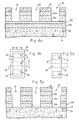
- a layer of resist 30 is next formed on the top polysilicon layer 28d and is exposed to a "slot" mask (dashed lines 32 in FIG. 4b), which simultaneously provides for mutual self-alignment between source 18, gate 22 and drain 20 regions.
- the slot mask 32 may also include provision for contact to other devices via extension 33 and for contact to the gate 22 via extension 35 and any other combinations thereof.
- It is a total level of interconnect, compared to conventional polysilicon, which is a half level. (The conventional half-level requires another level of interconnect to complete the connections.) In this manner, packing density of devices may be increased by nearly 50% over that of the prior art LOCOS process without critical alignment requirements. Further increases in density may be achieved as the technology of finer resist definition develops.
- the slot mask defines the polysilicon interconnect areas in the field and the source/gate/drain areas of all the devices.
- the slot masks can be at minimum feature and minimum feature spaces that may be defined lithographically. As can be seen, the source/gate/drain areas are self-aligned with each other so far.
- the resist 30 can be exposed by electromagnetic radiation (visible, UV, X-ray, as appropriate), as is conventional, and the undesired portions of the underlying four layers 28 are removed, such as by etching, to expose portions of the semiconductor substrate 16 corresponding to the source 18, gate 22 and drain 20 regions.
- the four layers 28 are etched as follows: First, the exposed portions of the polysilicon layer 28d are etched using an RIE etcher, followed by etching the exposed portions of the oxide layer 28c, again, using an RIE etcher. This latter etch stops at the nitride layer 28b, since the etch rate of the oxide can be adjusted with etch parameters to be about five times that of the nitride. This method of etching allows controlled manufacturability of the etch, since the nitride layer 28b acts as a built-in "buried" etch stop.
- the two etchings may be performed in one pump-down.
- the nitride layer 28b may be etched to the field oxide also, if it is desired to remove nitride from underneath the polysilicon layer 28d eventually.
- the RIE etch process employs a mixture of oxygen and fluorinated gas, such as CHF3, CF4, NF3, and the like. Controlled etch ratios between oxide and nitride are achieved by varying the ratio of the gases and, in some instances, the power of the etcher.
- the RIE etch process is well-known and thus does not per se form a part of this invention.
- the resist 30 is stripped and the wafer is remasked, using an "active" mask (denoted by solid lines 34 in FIG. 5b, the trench 10 being omitted for clarity) in conjunction with a new resist layer 36.
- an "active" mask denoted by solid lines 34 in FIG. 5b, the trench 10 being omitted for clarity
- the purpose of this mask is two-fold. First, in the source 18/gate 22/drain 20 areas, the etch is completed to silicon or to the exposed oxide in the slots. Some of this exposed oxide in the trenches 10 will be etched ( ⁇ 500 ⁇ ), corresponding to the required over-etch needed to clear the field oxide areas in the source 18, gate 22, and drain 20 openings down to the silicon substrate 16.
- the mask covers this with resist and prevents etching.
- the oxide 28a in the field region is ultimately retained under the polysilicon extensions 33, 35 in the field region, which is outside the area enclosed by the isolation trench 10 (including the trench oxide 26). This forms the polysilicon interconnections.
- the exposed portions of the nitride layer 28b are then etched, stopping on the field oxide layer 28a, again using RIE.
- the etch ratio is adjusted to greater than about 3:1 nitride to oxide.
- the exposed portions of the field oxide layer 28a are then etched, to expose portions of the underlying silicon 16. Again, as indicated above, the etching of the nitride layer 28b and oxide layer 28a can be done sequentially in one pump- down in the same etcher, merely changing chemistry to accommodate the nature of the respective layers.
- the use of the "buried etch stop" nitride layer 28b is seen to provide a unique solution to yet another etch sequence that enhances the process of the invention.
- a second etch then removes the nitride layer 28b, stopping on the field oxide 28a.
- the length of the channel (geometric), denoted L, has already been defined in the first etch, using the slot mask 32.
- the source 18, gate 22 and drain 20 regions have been defined geometrically, together with the device length L of the channel under the gate and the width W under the gate.
- the resist layer 36 is removed in a conventional manner and a thin oxide film 38 (the gate oxide) is grown in the exposed portions of the semiconductor substrate 16 (FIG. 6a).
- the gate oxide 38 as is conventional, is formed to a thickness of about 150 ⁇ 10 ⁇ , or less, depending on the scaling of the devices.
- a source/drain etch-out mask (denoted by solid lines 44 in FIG. 7b) is used to cover and protect the n-MOS gate areas, as shown at 42 in FIG. 7a.
- those portions of the gate oxide layer in the source 18, drain 20 areas are removed such as by a wet etch dip or by RIE etching or a combination thereof.
- the resist is then stripped off the wafer.
- a polysilicon layer is blanket-deposited to a thickness of about 7,000 ⁇ ⁇ 5% (for 1 ⁇ m feature widths) and then etched or polished (chemical/mechanical) back to stop on the upper oxide layer 28c.
- the polysiliccn fills all the source 18, gate 22 and drain 20 slots, as well as all the interconnect slots 32.
- the polysilicon filling the gate 22 slot is denoted 40g in FIG. 7a, and in connection with EPROM structures, is referred to as the floating gate).
- the polysilicon layer is polished back (chemical/mechanical), using the same apparatus as in silicon wafer polish, to planarize the polysilicon.
- the polysilicon gates 40g are not doped until the end of the process.
- an oxide layer 48 is formed everywhere, for example, thermally grown at about 900°C, typically to a thickness of about 125 ⁇ ⁇ 10%. This doubles as an ion implantation screen and a nitride etch stop, and accordingly, the thickness is governed by these considerations B11 ions are implanted to give P+ doping into the N+ areas that are open.
- a nitride layer 42 about 600 to 800 ⁇ thick (sufficient to mask POCl3) is deposited, masked using the N+ mask, and etched away together with the 125 ⁇ oxide layer 48 underneath to stop on polysilicon to expose N+ regions, which are then counter-doped with POCl3 (these regions were previously doped with boron).
- the N+ 44 mask (shown in FIG. 7b) employs nitride as the mask for N-MOS devices. As seen in FIG. 7a, the mask 42 protects the gate area 22 against doping. This is different compared to conventional N+ masks, wherein the source, gate and drain are all of the same doping; that is, the NMOS areas are completely opened and the gates are not protected.
- the N wells 12 are already in place prior to trench formation.
- the source and drain polysilicon plugs of each isolated region or device 14 are doped to a conductivity opposite that of the well 12 of that region, except where contacts to these are needed, they are then the same conductivity.
- the assembly is heated to about 900°C for about 60 min., to drive the dopants to form N+ junctions/regions for both sources 18 and drains 20 in the semiconductor.
- doped regions 18′, 20′ are formed by the drive.
- the temperature and time may be varied, depending on the plug depth and junction depth needed. Alternatively, a rapid thermal anneal may be used to drive the junctions.
- the gate is still undoped, since doping the gate polysilicon 40g would result in the dopant species penetrating the thin gate oxide 38 to the underlying semiconductor 16, and causing potential reliability problems.
- the masking nitride cap 42 is next removed over the gate areas 22.
- the three layers are planarized, with planarized polysilicon plugs 46s, 40g, 46d to sources 18, gates 22, and drains 20, respectively, on the semiconductor substrate 16. All sources, gates, drains and interconnects are mutually self-aligned.
- a novel contact scheme as described in detail below, can be implemented.
- the thickness of the polysilicon over the gate areas has to be scaled down to present reasonably planar or small step heights, as the aspect ratios get worse. A contact cannot be made directly on this gate over the gate oxide without degrading the gate breakdown.
- another aspect of the novel approach of this invention is that it allows a planar surface to be present at the contact-making step and at the metal deposition step immediately following it, which affords a manufacturing advantage at small geometries.
- the inventive approach also makes refill technologies and methods less demanding than conventional methods.
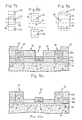
- An "anti-contact” resist mask (denoted by the crossed areas 50 in FIG. 8b) is formed as a layer 52 on the polysilicon layers 40g, 46s, 46d and patterned to cover the source 46s and drain 46d polysilicon and other desired regions of connectors.
- resist is left where the contacts are required, as distinct from a conventional contact mask where these contact areas are normally opened.
- the exposed portions of the polysilicon layer 46 are etched with a timed etch to remove a specific amount of polysilicon, using an etchant that has good selectivity to the underlying oxide is non-preferential with respect to N+ or undoped polysilicon.
- an etchant is chlorine-based plasma chemistry.
- about 4,000 ⁇ ⁇ 5% of polysilicon is removed. This amount will be the programming dielectric layer plus the control gate, the formation and purpose of which are discussed below.
- the contacts can overlap the oxide because the RIE polysilicon/oxide ratio evidences >20:1 selectivity.
- the contacts that are being defined are features in the resist and not openings in the resist as in conventional contact schemes, making lithography easier.
- FIG. 8a The resulting structure is shown in FIG. 8a. It will be seen that the polysilicon gate 40g is recessed by the etching, since it is an area that is not to be contacted. Other areas recessed by the etching (not shown) also will not be contacted.
- All the etched back areas at this stage have a similar width in one direction.
- the polysilicon in the gate is the width of the slot in which it resides (parallel to the plane of FIG. 8a). It is thus easy to fill these areas with spin-on glass to obtain a very flat topology as shown in FIG. 11a and as discussed in further detail below.
- the patterned resist 52 is removed, leaving contact to source 46s and drain 46d "buttons".
- a connector mask (denoted in FIG. 9b by solid lines 54) is employed to define portions 55 of the oxide layer 28c by use of a resist layer 57. These portions 55 are removed by etching, using the underlying nitride layer 28b as an etch stop. The exposed portions of the nitride layer 28b are then removed by etching, stopping on the field oxide layer 28a.
- this etch is identical to that discussed above in forming the interconnects and has all the advantages referred to therein.
- Implantations of appropriate ions are then done through the exposed portions of the field oxide 28a to connect and form the transistors (N-type). It will be noted that the oxide to be implanted through is the field oxide 28a, which has been deposited to a well-controlled thickness, as described above.
- the wafer is now implanted, using the N-mask, with phosphorus for the n-channels ( ⁇ 250 keV at 5x1014 cm ⁇ 2).
- the operation is done using the sequence of N-mask and etch, N-implant, and resist strip.
- the source 18′/drain 20′ junctions are now connected to the gate region 22′ (seen in FIG. 10a), completing the MOS FET device 14.
- the exrensions 24 are denoted "+".
- the gate polysilicon plugs 40g are also lightly doped with the same implant.
- the doping is driven slightly, such as at about 800° to 1,000°C for 15 to 30 seconds, by a rapid thermal anneal. This process activates the implants in the extensions 24 but does not cause excess diffusion of the implants, thereby avoiding penetration of the gate oxide 38. (The faster diffusion rates in polysilicon, however, allow substantially uniform doping of the gate polysilicon with this short cycle.) In this manner, N polysilicon plugs over the gates are formed.
- a layer 56 of inter-polysilicon dielectric is next grown over the exposed areas of polysilicon (46s, 46d, 40g) and oxide 28a therebetween, to form the programming dielectric.
- the dielectric layer may comprise (a) an oxide, such as silicon dioxide, ranging in thickness from about 100 to 200 ⁇ , (b) an oxy-nitride about 100 ⁇ thick formed by rapid thermal annealing of an oxide in ammonia, or (c) an oxide about 80 ⁇ thick over which is deposited a LPCVD layer ( ⁇ 800°C) of a nitride about 100 ⁇ thick, which oxide layer can be slightly oxidized (e.g., 50 ⁇ SiO2) to give an oxide/nitride/oxide structure to seal any pinholes in the nitride and give better dielectric integrity.
- the latter dielectric layers improve the break-down voltage of the inter poly layer 56 while improving the coupling between the poly layers 40g and 58 (discussed below) because of the higher dielectric constant.
- the structure is as shown in FIG. 11a. This dielectric layer 56 is used as an etch-stop in the step described below.
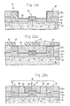
- a layer 58 of polysilicon is deposited everywhere and is polished back to be planar with the top of the sources 46s and drains 46d.
- the dielectric layer 56 also doubles as an etch-stop over the source 46s and drain 46d areas during the polish back.
- Layer 58 is termed the second poly level, and will comprise the control gate.
- a resist layer 60 is deposited and patterned to provide openings 62 to expose portions of the poly layer 58, as shown in FIG. 12a.
- the exposed portions of polysilicon 58 are etched back to stop on the dielectric layer 56, forming openings 62. All exposed portions of the dielectric layer 56 are then etched away, the resist layer 60 is stripped, and the openings 62 are filled with oxide 64 to form an EPROM element 66, shown in FIG. 13a.
- control gate 58 in this manner, together with the overlap of the floating gate 40g enables coupling between the two electrodes to take place both in the horizontal interface between the two and in the vertical sidewall areas of the interfaces.
- Contacts may be made to the source 46s, drain 46d, and control gate 58 by means well-known in the art.
- tungsten may be used in place of polysilicon, such as for the source/drain contacts. If tungsten is employed, then the process should be modified to implant the substrate first, then deposit tungsten. In this modification, any polysilicon used, such as in the gates, would also be deposited after implant of the substrate, and any subsequent implant would be to dope the polysilicon, not to form any junctions. The intersection of the polysilicon gates and tungsten interconnect will be ohmic, due to the formation of tungsten polysilicide at this intersection.
- FIG. 13a The structure shown in FIG. 13a is an N-channel transistor with the floating gate 40g and control gate 58 capacitively coupled (as distinct from electrically coupled) through the dielectric 56.
- the basic premise is that the device 66 has two threshold voltages: one related to the operation of a "normal” N-channel transistor and the other related to a "programmed” threshold, following programming of the transistor.
- the source 46s is at 0 V (ground), the drain 46d is at least 5 V and the voltage on the control gate 58 (V GS ) is equal to or less than that on the drain. Due to the capacitive coupling between the floating gate 40g and the control gate 58, the potential on the floating gate is substantially the same as that on the control gate.
- the current characteristics of the device diagrammatically shown in FIG. 14, are considered "normal" for a transistor. The electrons flow from the source 46s to the drain 46d, as illustrated in FIG. 15a.
- control gate voltage is made more positive (for example, at least twice the drain voltage, or about 11 to 13 V)
- the electrons are drawn into the gate oxide 38, as illustrated in FIG. 15b.
- the trapped electrons invert the p-type silicon at the surface so that an n-type surface layer is formed, having the characteristics diagrammatically shown in FIG. 14b. Consequently, the threshold voltage of the device is lowered.
- a determination of whether the device is programmed may be made.
- the EPROM element 66 may be erased by shining UV radiation thereon. Electrons trapped in the gate oxide 38 are made to recombine with holes generated by the UV radiation. This restores the threshold voltage of the device to its pre-programmed level.
Landscapes
- Non-Volatile Memory (AREA)
- Insulated Gate Type Field-Effect Transistor (AREA)
- For Increasing The Reliability Of Semiconductor Memories (AREA)
Applications Claiming Priority (4)
| Application Number | Priority Date | Filing Date | Title |
|---|---|---|---|
| US16282288A | 1988-03-02 | 1988-03-02 | |
| US162822 | 1988-03-02 | ||
| US07/276,278 US4964143A (en) | 1988-03-02 | 1988-11-23 | EPROM element employing self-aligning process |
| US276278 | 1988-11-23 |
Publications (2)
| Publication Number | Publication Date |
|---|---|
| EP0331418A2 true EP0331418A2 (de) | 1989-09-06 |
| EP0331418A3 EP0331418A3 (de) | 1990-08-08 |
Family
ID=26859088
Family Applications (1)
| Application Number | Title | Priority Date | Filing Date |
|---|---|---|---|
| EP89301957A Ceased EP0331418A3 (de) | 1988-03-02 | 1989-02-28 | EPROM-Programmierungselemente |
Country Status (3)
| Country | Link |
|---|---|
| US (1) | US4964143A (de) |
| EP (1) | EP0331418A3 (de) |
| JP (1) | JPH0277168A (de) |
Cited By (4)
| Publication number | Priority date | Publication date | Assignee | Title |
|---|---|---|---|---|
| EP0473129A3 (en) * | 1990-08-29 | 1993-02-03 | Texas Instruments Incorporated | Asymmetrical non-volatile memory cell, arrays and methods for fabricating same |
| EP0597124A4 (de) * | 1992-05-29 | 1995-02-15 | Citizen Watch Co Ltd | Nichtflüchtige halbleiterspeicheranordnung, halbleiteranordnung und verfahren zur herstellung. |
| US5612914A (en) * | 1991-06-25 | 1997-03-18 | Texas Instruments Incorporated | Asymmetrical non-volatile memory cell, arrays and methods for fabricating same |
| CN101621030B (zh) * | 2008-07-02 | 2011-01-12 | 中芯国际集成电路制造(上海)有限公司 | 具有多晶硅接触的自对准mos结构 |
Families Citing this family (16)
| Publication number | Priority date | Publication date | Assignee | Title |
|---|---|---|---|---|
| GB8907898D0 (en) | 1989-04-07 | 1989-05-24 | Inmos Ltd | Semiconductor devices and fabrication thereof |
| US5172200A (en) * | 1990-01-12 | 1992-12-15 | Mitsubishi Denki Kabushiki Kaisha | MOS memory device having a LDD structure and a visor-like insulating layer |
| US5202850A (en) * | 1990-01-22 | 1993-04-13 | Silicon Storage Technology, Inc. | Single transistor non-volatile electrically alterable semiconductor memory device with a re-crystallized floating gate |
| EP0464196B1 (de) * | 1990-01-22 | 2002-05-08 | Silicon Storage Technology, Inc. | Nichtflüchtige elektrisch veränderbare eintransistor-halbleiterspeicheranordnung mit rekristallisiertem schwebendem gate |
| US5067108A (en) * | 1990-01-22 | 1991-11-19 | Silicon Storage Technology, Inc. | Single transistor non-volatile electrically alterable semiconductor memory device with a re-crystallized floating gate |
| US5162884A (en) * | 1991-03-27 | 1992-11-10 | Sgs-Thomson Microelectronics, Inc. | Insulated gate field-effect transistor with gate-drain overlap and method of making the same |
| US5281548A (en) * | 1992-07-28 | 1994-01-25 | Micron Technology, Inc. | Plug-based floating gate memory |
| US5640031A (en) * | 1993-09-30 | 1997-06-17 | Keshtbod; Parviz | Spacer flash cell process |
| US5479368A (en) * | 1993-09-30 | 1995-12-26 | Cirrus Logic, Inc. | Spacer flash cell device with vertically oriented floating gate |
| KR100211072B1 (ko) * | 1996-12-28 | 1999-07-15 | 구본준 | 플래쉬 메모리 셀의 제조방법 |
| US6121088A (en) | 1998-09-17 | 2000-09-19 | Taiwan Semiconductor Manufacturing Company | Method of manufacture of undoped polysilicon as the floating-gate of a split-gate flash cell |
| US7642566B2 (en) * | 2006-06-12 | 2010-01-05 | Dsm Solutions, Inc. | Scalable process and structure of JFET for small and decreasing line widths |
| US6686247B1 (en) | 2002-08-22 | 2004-02-03 | Intel Corporation | Self-aligned contacts to gates |
| US7247907B2 (en) * | 2005-05-20 | 2007-07-24 | Silicon Storage Technology, Inc. | Bidirectional split gate NAND flash memory structure and array, method of programming, erasing and reading thereof, and method of manufacturing |
| DE102013214214A1 (de) * | 2013-07-19 | 2015-01-22 | Fraunhofer-Gesellschaft zur Förderung der angewandten Forschung e.V. | Verfahren zum Löschen von Informationen und Vorrichtung zur Durchführung desselben |
| KR102300122B1 (ko) * | 2015-02-17 | 2021-09-09 | 에스케이하이닉스 주식회사 | 전하 트랩 불휘발성 메모리소자 및 그 제조방법과, 전하 트랩 불휘발성 메모리소자의 동작방법 |
Family Cites Families (7)
| Publication number | Priority date | Publication date | Assignee | Title |
|---|---|---|---|---|
| US3984822A (en) * | 1974-12-30 | 1976-10-05 | Intel Corporation | Double polycrystalline silicon gate memory device |
| US4288256A (en) * | 1977-12-23 | 1981-09-08 | International Business Machines Corporation | Method of making FET containing stacked gates |
| US4231051A (en) * | 1978-06-06 | 1980-10-28 | Rockwell International Corporation | Process for producing minimal geometry devices for VSLI applications utilizing self-aligned gates and self-aligned contacts, and resultant structures |
| US4355455A (en) * | 1979-07-19 | 1982-10-26 | National Semiconductor Corporation | Method of manufacture for self-aligned floating gate memory cell |
| JPS60189971A (ja) * | 1984-03-09 | 1985-09-27 | Toshiba Corp | 半導体装置の製造方法 |
| JPS61105862A (ja) * | 1984-10-30 | 1986-05-23 | Toshiba Corp | 半導体装置 |
| JPS61136274A (ja) * | 1984-12-07 | 1986-06-24 | Toshiba Corp | 半導体装置 |
-
1988
- 1988-11-23 US US07/276,278 patent/US4964143A/en not_active Expired - Lifetime
-
1989
- 1989-02-28 EP EP89301957A patent/EP0331418A3/de not_active Ceased
- 1989-03-01 JP JP1049766A patent/JPH0277168A/ja active Pending
Cited By (5)
| Publication number | Priority date | Publication date | Assignee | Title |
|---|---|---|---|---|
| EP0473129A3 (en) * | 1990-08-29 | 1993-02-03 | Texas Instruments Incorporated | Asymmetrical non-volatile memory cell, arrays and methods for fabricating same |
| US5674764A (en) * | 1990-08-29 | 1997-10-07 | Texas Instruments Incorporated | Method of making asymmetric non-volatile memory cell |
| US5612914A (en) * | 1991-06-25 | 1997-03-18 | Texas Instruments Incorporated | Asymmetrical non-volatile memory cell, arrays and methods for fabricating same |
| EP0597124A4 (de) * | 1992-05-29 | 1995-02-15 | Citizen Watch Co Ltd | Nichtflüchtige halbleiterspeicheranordnung, halbleiteranordnung und verfahren zur herstellung. |
| CN101621030B (zh) * | 2008-07-02 | 2011-01-12 | 中芯国际集成电路制造(上海)有限公司 | 具有多晶硅接触的自对准mos结构 |
Also Published As
| Publication number | Publication date |
|---|---|
| JPH0277168A (ja) | 1990-03-16 |
| EP0331418A3 (de) | 1990-08-08 |
| US4964143A (en) | 1990-10-16 |
Similar Documents
| Publication | Publication Date | Title |
|---|---|---|
| US4964143A (en) | EPROM element employing self-aligning process | |
| US7045413B2 (en) | Method of manufacturing a semiconductor integrated circuit using a selective disposable spacer technique and semiconductor integrated circuit manufactured thereby | |
| JP3623804B2 (ja) | イオンが注入された構造体および形成方法 | |
| JP4065414B2 (ja) | 埋設ソースライン及びフローティングゲートを伴うフローティングゲートメモリセルの半導体メモリアレーを形成する自己整列型方法及びそれにより作られたメモリアレー | |
| JP4388266B2 (ja) | ストラップ領域及び周辺論理デバイス領域を有するフローティングゲートメモリセルの半導体アレーを形成する方法 | |
| US6750090B2 (en) | Self aligned method of forming a semiconductor memory array of floating gate memory cells with floating gates having multiple sharp edges, and a memory array made thereby | |
| US6271087B1 (en) | Method for forming self-aligned contacts and local interconnects using self-aligned local interconnects | |
| US6562681B2 (en) | Nonvolatile memories with floating gate spacers, and methods of fabrication | |
| US4977108A (en) | Method of making self-aligned, planarized contacts for semiconductor devices | |
| US5081516A (en) | Self-aligned, planarized contacts for semiconductor devices | |
| US5091326A (en) | EPROM element employing self-aligning process | |
| US5028555A (en) | Self-aligned semiconductor devices | |
| JPH10511510A (ja) | 側壁スペーサを使用するメモリアレーのための自己整列型トレンチアイソレーション | |
| US20020151141A1 (en) | Dummy structures that protect circuit elements during polishing | |
| US4974055A (en) | Self-aligned interconnects for semiconductor devices | |
| US6967372B2 (en) | Semiconductor memory array of floating gate memory cells with vertical control gate sidewalls and insulation spacers | |
| EP0344292B1 (de) | Ein verfahren zur herstellung selbstausrichtender halbleiteranordnungen | |
| US5055427A (en) | Process of forming self-aligned interconnects for semiconductor devices | |
| US5057902A (en) | Self-aligned semiconductor devices | |
| US7384845B2 (en) | Methods of fabricating flash memory devices including word lines with parallel sidewalls | |
| US6482699B1 (en) | Method for forming self-aligned contacts and local interconnects using decoupled local interconnect process | |
| US6495853B1 (en) | Self-aligned gate semiconductor | |
| US6878622B1 (en) | Method for forming SAC using a dielectric as a BARC and FICD enlarger | |
| US6228716B1 (en) | Method of making damascene flash memory transistor | |
| US20040079984A1 (en) | Polysilicon self-aligned contact and a polysilicon common source line and method of forming the same |
Legal Events
| Date | Code | Title | Description |
|---|---|---|---|
| PUAI | Public reference made under article 153(3) epc to a published international application that has entered the european phase |
Free format text: ORIGINAL CODE: 0009012 |
|
| AK | Designated contracting states |
Kind code of ref document: A2 Designated state(s): AT BE CH DE ES FR GB GR IT LI LU NL SE |
|
| PUAL | Search report despatched |
Free format text: ORIGINAL CODE: 0009013 |
|
| AK | Designated contracting states |
Kind code of ref document: A3 Designated state(s): AT BE CH DE ES FR GB GR IT LI LU NL SE |
|
| 17P | Request for examination filed |
Effective date: 19901217 |
|
| 17Q | First examination report despatched |
Effective date: 19920421 |
|
| STAA | Information on the status of an ep patent application or granted ep patent |
Free format text: STATUS: THE APPLICATION HAS BEEN REFUSED |
|
| 18R | Application refused |
Effective date: 19930603 |