EP0329101B1 - Three-dimensional graphic processing apparatus - Google Patents
Three-dimensional graphic processing apparatus Download PDFInfo
- Publication number
- EP0329101B1 EP0329101B1 EP89102578A EP89102578A EP0329101B1 EP 0329101 B1 EP0329101 B1 EP 0329101B1 EP 89102578 A EP89102578 A EP 89102578A EP 89102578 A EP89102578 A EP 89102578A EP 0329101 B1 EP0329101 B1 EP 0329101B1
- Authority
- EP
- European Patent Office
- Prior art keywords
- values
- value
- intensity
- depth coordinate
- coordinate
- Prior art date
- Legal status (The legal status is an assumption and is not a legal conclusion. Google has not performed a legal analysis and makes no representation as to the accuracy of the status listed.)
- Expired - Lifetime
Links
Images


Classifications
-
- G—PHYSICS
- G06—COMPUTING; CALCULATING OR COUNTING
- G06F—ELECTRIC DIGITAL DATA PROCESSING
- G06F7/00—Methods or arrangements for processing data by operating upon the order or content of the data handled
- G06F7/38—Methods or arrangements for performing computations using exclusively denominational number representation, e.g. using binary, ternary, decimal representation
- G06F7/48—Methods or arrangements for performing computations using exclusively denominational number representation, e.g. using binary, ternary, decimal representation using non-contact-making devices, e.g. tube, solid state device; using unspecified devices
- G06F7/544—Methods or arrangements for performing computations using exclusively denominational number representation, e.g. using binary, ternary, decimal representation using non-contact-making devices, e.g. tube, solid state device; using unspecified devices for evaluating functions by calculation
- G06F7/548—Trigonometric functions; Co-ordinate transformations
-
- G—PHYSICS
- G06—COMPUTING; CALCULATING OR COUNTING
- G06T—IMAGE DATA PROCESSING OR GENERATION, IN GENERAL
- G06T15/00—3D [Three Dimensional] image rendering
- G06T15/50—Lighting effects
- G06T15/80—Shading
- G06T15/87—Gouraud shading
Definitions
- the present invention relates to a three-dimensional graphic processing apparatus for performing shading of a graphic pattern constituted by a plurality of polygons.
- Gouraud shading is well known as an algorithm for performing three-dimensional display by processing called shading.
- the three-dimensional shading display obtained by the Gouraud shading will be described below.
- information of a polygon is given.
- the contents of the information are three-dimensional coordinate values and a intensity value of each vertex of the polygon.
- information (x,y,z,I) containing three-dimensional coordinate values and a intensity value about a vertex A is (x1,y1,z1,I1)
- that about a vertex B is (x2,y2,z2,I2)
- that about a vertex C is (x3,y3,z3,I3).
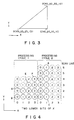
- reference numeral 40 denotes a scan line parallel to the X coordinate axis
- intensity values, X and Y coordinate values, and Z coordinate values representing the depths must be calculated for pixels along the scan line 40.
- An intensity value I and the Z coordinate value can be calculated by interpolation calculations.
- an intensity value I4 of a pixel D at a three-dimensional coordinate point (x4,y4,z4) as an intersection point of the line 40 and a side BC of the triangle polygon can be obtained by an interpolation calculation of vertexes B and C
- a intensity value I5 of a pixel E at a three-dimensional coordinate point (x5,y5,z5) as an intersection point of the line 40 and a side AC can be obtained by an interpolation calculation of vertexes A and C.
- I4 I2( y4 - y3 y2 - y3 ) + I3( y2 - y4 y2 - y3 )
- I5 I1( y5 - y3 y1 - y3 ) + I3( y1 - y5 y1 - y3 )
- An intensity value at an arbitrary pixel F on the line 40 can be obtained by an interpolation calculation of the intensity values I4 and I5.
- Z coordinate values and intensity values of pixels on each scan line are sequentially calculated by a single arithmetic IC per pixel. Calculation results are then written in a display memory to perform painting of a graphic pattern.
- An access speed of the memory is lower than a calculation speed of the calculation IC, and a throughput of the entire apparatus is therefore determined by the access speed. Since the number of pixels constituting a three-dimensional graphic pattern is very large, shading requires a very long time in the conventional apparatus because an access speed of a memory is generally low.
- the present invention provides a three-dimensional graphic processing apparatus as specified in claim 1.
- reference numerals 10A, 10B, 10C and 10D denote arithmetic ICs for calculating an inclination ⁇ Z of Z coordinates and an inclination ⁇ I of intensity values on the polygon plane, calculating a Z coordinate value and a intensity value I of a point from which painting is started on each scan line parallel to the X coordinate axis and which is present on one of three sides defining the triangle polygon, and sequentially calculating Z coordinate values and intensity values I of different points on a single scan line, thereby performing shading and hidden surface removal.
- the arithmetic ICs 10A, 10B, 10C and 10D are assigned with numbers of 0, 1, 2 and 3, respectively.
- the Z coordinate values and the intensity values I calculated and subjected to hidden surface removal by the ICs, 10A, 10B, 10C and 10D are stored in four Z memories 11A, 11B, 11C and 11D, and four I memories 12A, 12B, 12C and 12D, respectively.
- Each of the ICs 10A, 10B, 10C and 10D outputs a write pulse for storing a calculation result to a corresponding one of each of the Z memories 11 and the I memories 12. Note that in the above hidden surface removal, a smallest Z coordinate value of a polygon is selected. A polygon subjected to the hidden surface removal is present closest on a display screen.
- Each pixel on each scan line is assigned with X-and Y-coordinate addresses.
- Z coordinate values and intensity values I of pixels in which two lower bits at the X-coordinate addresses represent numbers 0, 1, 2 and 3 are calculated by the arithmetic ICs 10A, 10B, 10C and 10D assigned with the numbers 0, 1, 2 and 3, respectively.
- the numbers 0, 1, 2 and 3 assigned to the respective pixels are written in the circles representing the pixels in Fig. 4 to be calculated by the ICs 10A, 10B, 10C and 10D.
- a processing cycle for executing calculations by the ICs 10A, 10B, 10C and 10D is performed twice or once, and a processing cycle for painting is performed twice or once for each scan line from the first scan line. That is, in a processing cycle 1 for a single scan line, Z coordinate values and intensity values of four successive pixels are parallelly calculated by the four arithmetic ICs 10A, 10B, 10C and 10D.
- each IC checks how far its calculation point is offset from a start point of linear interpolation on the X coordinate axis. This check is performed by comparing two lower bits at an address of an X coordinate of the start point of linear interpolation with the number assigned to each arithmetic IC 10.
- Each of the ICs 10A, 10B, 10C and 10D adds a correction value of intensity corresponding to a difference of the X coordinate shown in Fig. 5 to the calculated intensity value I of the painting start point (each pixel on a side AB of the triangle) on the scan line, and adds a correction value of a Z coordinate value corresponding to a difference of the X coordinate shown in Fig. 6 to a Z coordinate value of the start point.
- the arithmetic ICs check to which IC the painting start point on the scan line corresponds. On the basis of this check result, values shown in Fig. 7 are added as final correction values to the intensity values and Z coordinate values.
- Z coordinate values and intensity values I of four successive pixels are parallelly calculated by the ICs 10A, 10B, 10C and 10D.
- each IC 10 adds 4 ⁇ I and 4 ⁇ Z to the intensity value and the Z coordinate value at each point calculated in the processing cycle 1.
- Such calculations are performed for each scan line, and calculation results are sequentially supplied to a corresponding one of each of the Z memories 11 and the I memories 12.
- each arithmetic IC 10 checks how far its calculation point is offset from a start point (vertex B) of linear interpolation on the X coordinate axis.
- a calculation point of the IC 10A is the start point of the linear interpolation and a number represented by two lower bits at an address of an X coordinate and the number assigned to the IC 10A are both 0s
- a difference between both the points on the X coordinate axis is 0.
- differences between calculation points of the ICs 10B, 10C and 10D and the start point of the linear interpolation on the X coordinate axis are 1, 2 and 3, respectively.
- each IC 10 determines that a value of two lower bits at an address of an X coordinate of the painting start point is 0 on the first scan line and coincides with the number 0 assigned to the IC 10A.
- the ICs 10A, 10B, 10C and 10D add correction values 0, ⁇ , 2 ⁇ , 3 ⁇ in a column where the value of the two lower bits of the X coordinate is 0 in Fig. 7 to an intensity value and a Z coordinate value at the painting start point, respectively.
- IC Nos. in Fig. 7 correspond to the numbers assigned to the ICs 10A, 10B, 10C and 10D.
- the arithmetic ICs 10A, 10B, 10C and 10D parallelly add 4 ⁇ I and 4 ⁇ Z to the intensity values and the Z coordinate values of the respective points calculated in the processing cycle 1, thereby calculating intensity values I and Z coordinate values of four successive pixels.
- each arithmetic IC 10 checks how far its calculation point is offset from a start point (D in Fig. 4) of linear interpolation on the X coordinate axis.
- a difference between a calculation point of the IC 10B, assigned with the number 1, for calculating the linear interpolation start point D and the start point D is 0.
- the ICs 10A, 10B, 10C and 10D add correction values - ⁇ , 0, ⁇ and 2 ⁇ in a column where the value of the two lower bits of the X coordinate is 1 in Fig. 7 to an intensity value and a Z coordinate value at the painting start point D, respectively.
- the ICs 10A, 10B, 10C and 10D parallelly add 4 ⁇ I and 4 ⁇ Z to the intensity values and the Z coordinate values of the pixels calculated in the processing cycle 1, thereby calculating intensity values I and Z coordinate values of four successive pixels.
- each arithmetic IC 10 checks how far its calculation point is offset from a start point (E in Fig. 4) of linear interpolation on the X coordinate axis.
- a difference between a calculation point of the IC 10C, assigned with the number 2, for calculating the linear interpolation start point E and the start point E is 0.
- the ICs 10A, 10B, 10C and 10D add correction values -2 ⁇ , - ⁇ , 0 and ⁇ in a column where the value of the two lower bits of the X coordinate is 2 in Fig. 7 to an intensity value and a Z coordinate value at the painting start point E, respectively.
- the ICs 10A, 10B, 10C and 10D parallelly add 4 ⁇ I and 4 ⁇ Z to the intensity values and the Z coordinate values of the pixels calculated in the processing cycle 1, thereby calculating intensity values I and Z coordinate values of four successive pixels.
- each arithmetic IC 10 checks how far its calculation point is offset from a start point (F in Fig. 4) of linear interpolation on the X coordinate axis.
- a difference between a calculation point of the IC 10D, assigned with the number 3, for calculating the linear interpolation start point F and the start point F is 0.
- the ICs 10A, 10B, 10C and 10D add correction values -3 ⁇ , -2 ⁇ , - ⁇ and 0 in a column where the value of the two lower bits of the X coordinate is 3 in Fig. 7 to an intensity value and a Z coordinate value at the painting start point E, respectively.
- the ICs 10A, 10B, 10C and 10D parallelly add 4 ⁇ I and 4 ⁇ Z to the intensity values and the Z coordinate values of the pixels calculated in the processing cycle 1, thereby calculating intensity values I and Z coordinate values of four successive pixels. In this manner, the intensity values I and the Z coordinate values of pixels on each scan line of the triangle polygon as shown Fig. 4 are calculated.
- Z coordinate values and intensity values I of the pixels present outside the polygon need not be stored in the Z memories 11 and the I memories 12. Storage of the Z coordinate values and the intensity values I is performed upon supply of write pulses from the ICs 10 to the Z memories 11 and the I memories 12.
- each IC 10 checks whether its calculation point is present in the polygon and outputs the write pulse only when the point is present in the polygon. This check is performed by each IC as follows.
- a processing cycle is a start cycle (i.e., the processing cycle 1 of any of the first to fourth scan lines in Fig. 4), it is compared two lower bits at an address of an X coordinate of start point of linear interpolation with the number assigned to each arithmetic IC. On the basis of this result, each IC outputs a write pulse in accordance with a rule shown in Fig. 8.
- a value of two lower bits of the start point of linear interpolation is 0.
- a value of two lower bits of the start point of linear interpolation is 1.
- a column where the value of the two lower bits at the X coordinate is 1 in Fig. 8 is referred to.
- the value of the IC having the number 0 is 0, and those of the other ICs are 1s. Therefore, the ICs 10B, 10C and 10D except for the IC 10A output write pulses.
- a value of two lower bits of the start point of linear interpolation is 2. At this time, a column where the value of the two lower bits at the X coordinate is 2 in Fig. 8 is referred to.
- the ICs 10C and 10D corresponding to the numbers 2 and 3 output write pulses.
- a value of two lower bits of the start point of linear interpolation is 3.
- a column where the value of the two lower bits at the X coordinate is 3 in Fig. 8 is referred to.
- only the IC 10D corresponding to the number 3 outputs a write pulse.
- a processing cycle is an end cycle (i.e., the processing cycle 2 of any of the first to fourth scan lines in Fig. 4), it is compared two lower bits at an address of an X cordinate of end point of linear interpolation with the number assigned to each arithmetic IC. On the basis of this result, each IC 10 outputs a write pulse in accordance with a rule shown in Fig. 9.
- a value of two lower bits of an end point of linear interpolation is 1.
- a column where the value of the two lower bits at the X coordinate is 1 in Fig. 9 is referred to.
- the ICs 10A and 10B corresponding to the numbers 0 and 1 output write pulses. Thereafter, to the fifth scan line, the ICs 10A and 10B corresponding to the numbers 0 and 1 output write pulses in the same manner as described above.
- write pulses are output on the basis of values of logical AND products of the values of the rules shown in Figs. 8 and 9. That is, when the fifth scan line is to be processed, a value of two lower bits of the start point of linear interpolation is 0. At this time, a column where the value of the two lower bits at the X coordinate is 0 in Fig. 8 is referred to. In this case, values corresponding to all the ICs are 1s. A value of two lower bits of an end point of linear interpolation is then 1. At this time, a column where the value of the two lower bits at the X coordinate is 1 in Fig. 9 is referred to.
- values corresponding to the ICs having the numbers 0 and 1 are 1s.
- values of the ICs having the numbers 0 and 1 become 1s, and the arithmetic ICs 10A and 10B output write pulses accordingly.
- a value of two lower bits of the start point of linear interpolation is 1.
- a column where the value of the two lower bits at the X coordinate is 1 in Fig. 8 is referred to.
- values corresponding to the ICs having the numbers 1, 2 and 3 are 1s.
- a value of two lower bits of the end point of linear interpolation is 1.
- a column where the value of the two lower bits at the X coordinate is 1 in Fig. 9 is referred to.
- values corresponding to the ICs having the numbers 0 and 1 are 1s.
- a logical value corresponding to the IC having the number 1 becomes 1, and only the IC 10B outputs a write pulse accordingly.
- Fig. 10 is a block diagram showing an arrangement of a main part of each arithmetic IC used in the apparatus of the above embodiment.
- reference numeral 21 denotes an arithmetic controller.
- the controller 21 receives information concerning one of the numbers 0, 1, 2 and 3 of the corresponding IC, the two lower bits at an address of the X coordinate, and a vertex of the triangle polygon. On the basis of these inputs, the controller 21 calculates correction values 0, ⁇ I, 2 ⁇ I and 3 ⁇ I of the intensity as shown in Fig. 5, correction values 0, ⁇ Z, 2 ⁇ Z and 3 ⁇ Z of the Z coordinate as shown in Fig.
- the initial values Ii and Zi of the intensity and the Z coordinate calculated by the controller 21 are supplied to and temporarily stored in registers 22 and 23, respectively.
- the correction values 0, ⁇ I, 2 ⁇ I and of the intensity calculated by the controller 21 are supplied to and temporarily stored in a register 24.
- the correction values 0, ⁇ Z, 2 ⁇ Z and 3 ⁇ Z of the Z coordinate calculated by the controller 21 are supplied to and temporarily stored in a register 25.
- the inclinations ⁇ I′ and ⁇ Z′ of the intensity value I and the Z coordinate of the left side of the triangle polygon calculated by the controller 21 are supplied to and temporarily stored in registers 26 and 27, respectively.
- the values of 4 ⁇ I and 4 ⁇ Z calculated by the controller 21 are supplied to and temporarily stored in registers 28 and 29, respectively.
- the controller 21 performs read control of the values stored in the registers 22 to 29.
- reference numeral 30 denotes a selector; 31, an adder/subtractor; 32 and 33, selectors; 34 and 35, registers for storing outputs from the selectors 32 and 33, respectively; and 36 and 37, adders. Operations of the selector 30, the adder/subtractor 31, the selectors 32 and 33, the registers 34 and 35, and the adders 36 and 37 are also controlled by the controller 21.
- the correction value in the register 24 designated by the controller 21 is supplied to the adder/subtractor 31 via the selector 30.
- the adder/subtractor 31 performs addition or subtraction between the input initial value Ii of the intensity and the correction value read out from the register 24, thereby calculating a intensity value at a start point of a calculation according to the rule shown in Fig. 7.
- the calculated intensity value is stored in the register 34 via the selector 32.
- the initial value Zi of the Z coordinate at the vertex B of the polygon stored in the register 23 is then supplied to the adder/subtractor 31.
- the controller 21 designates a correction value of the Z coordinate stored in the register 25.
- the correction value in the register 25 designated by the controller 21 is supplied to the adder/subtractor 31 via the selector 30.
- the adder/subtractor 31 performs addition or subtraction between the initial value Zi of the Z coordinate and the correction value read out from the register 25, thereby calculating a Z coordinate value at the calculation start point according to the rule shown in Fig. 7.
- the calculated Z coordinate value is stored in the register 35 via the selector 33.
- the horizontal operation is started. The horizontal operation will be performed as shown in Fig. 12.
- the adder 36 adds the value of 4 ⁇ I stored in the register 28 to the initial value of the intensity stored in the register 34, and the addition result is supplied to the I memory.
- the adder 37 adds the value of 4 ⁇ Z stored in the register 29 to the initial value of the Z coordinate of the linear interpolation calculation stored in the register 35, and the addition result is supplied to the Z memory. Thereafter, in accordance with the rule shown in Fig. 8 or 9 or a logical AND product of the values of both the rules, the controller 21 generates a write pulse. Thereafter, an address of the X coordinate is incremented by four. At this time, if the address of the X coordinate is smaller than a coordinate at the right end of the scan line, the horizontal operation is determined to be Busy, and the flow returns to the start of the operation.
- Intensity values and Z coordinate values of pixels on second and subsequent scan lines are calculated as follows. First, the intensity value Ii stored in the register 22 and the inclination ⁇ I′ of the intensity value stored in the register 26 are supplied to the adder/subtractor 31. The adder/subtractor 31 adds the values from the registers 22 and 26 to calculate a intensity value at a start point of a calculation on the next scan line. The calculated intensity value is stored in the register 22 again. After correction at the start point is performed using the value shown in Fig. 7, this corrected intensity value is supplied to the register 34 via the selector 32.
- the Z coordinate value Zi stored in the register 23 and the inclination ⁇ Z′ of the Z coordinate value stored in the register 27 are supplied to the adder/subtractor 31.
- the adder/subtractor 31 adds the values from the registers 23 and 27 to calculate a Z coordinate value at the calculation start point on the next scan line.
- the calculated Z coordinate value is stored in the register 23 again. After correction at the start point is performed using the value shown in Fig. 7, this corrected Z coordinate value is supplied to the register 35 via the selector 33.
- the adder 36 sequentially adds the value of 4 ⁇ I to the intensity value stored in the register 34 in each processing cycle.
- the adder 37 sequentially adds the value of 4 ⁇ Z to the Z coordinate value stored in the register 35 in each processing cycle.
- the present invention is not limited to the above embodiment but can be variously modified.
- four arithmetic ICs are used to parallelly calculate intensity values and Z coordinate values of pixels. Since the object of the present invention, however, can be achieved by two or more arithmetic ICs, the number of the arithmetic ICs may be any number more than one.
- a triangle polygon consisting of 21 pixels as in Fig. 4 is parallelly processed using two arithmetic ICs. In this case, although 12 processing cycles are required, this number of the processing cycles is much smaller than conventional 21 cycles.
- Fig. 14 shows values corresponding to those in Fig. 7 obtained using two arithmetic ICs.
- a correction value is any of 0, ⁇ or - ⁇ .
Landscapes
- Engineering & Computer Science (AREA)
- Physics & Mathematics (AREA)
- General Physics & Mathematics (AREA)
- Theoretical Computer Science (AREA)
- Mathematical Analysis (AREA)
- Computational Mathematics (AREA)
- Computer Graphics (AREA)
- Mathematical Optimization (AREA)
- Pure & Applied Mathematics (AREA)
- Mathematical Physics (AREA)
- Computing Systems (AREA)
- General Engineering & Computer Science (AREA)
- Image Generation (AREA)
Applications Claiming Priority (2)
| Application Number | Priority Date | Filing Date | Title |
|---|---|---|---|
| JP63033437A JP2618951B2 (ja) | 1988-02-16 | 1988-02-16 | 三次元図形処理装置 |
| JP33437/88 | 1988-02-16 |
Publications (3)
| Publication Number | Publication Date |
|---|---|
| EP0329101A2 EP0329101A2 (en) | 1989-08-23 |
| EP0329101A3 EP0329101A3 (en) | 1992-01-08 |
| EP0329101B1 true EP0329101B1 (en) | 1995-06-28 |
Family
ID=12386512
Family Applications (1)
| Application Number | Title | Priority Date | Filing Date |
|---|---|---|---|
| EP89102578A Expired - Lifetime EP0329101B1 (en) | 1988-02-16 | 1989-02-15 | Three-dimensional graphic processing apparatus |
Country Status (5)
| Country | Link |
|---|---|
| US (1) | US5163127A (ja) |
| EP (1) | EP0329101B1 (ja) |
| JP (1) | JP2618951B2 (ja) |
| KR (1) | KR920007507B1 (ja) |
| DE (1) | DE68923191T2 (ja) |
Families Citing this family (20)
| Publication number | Priority date | Publication date | Assignee | Title |
|---|---|---|---|---|
| JPH0758510B2 (ja) * | 1989-10-31 | 1995-06-21 | 株式会社東芝 | 三次元図形処理装置 |
| KR100232931B1 (ko) * | 1989-12-21 | 1999-12-01 | 이데이 노부유끼 | 컴퓨터 그래픽용 쉐이딩 방법 및 시스템 |
| DE69122557T2 (de) * | 1990-06-29 | 1997-04-24 | Philips Electronics Nv | Bilderzeugung |
| US5420972A (en) * | 1990-11-15 | 1995-05-30 | International Business Machines Corporation | Method and apparatus for rendering lines |
| US5343558A (en) * | 1991-02-19 | 1994-08-30 | Silicon Graphics, Inc. | Method for scan converting shaded triangular polygons |
| US5706415A (en) * | 1991-12-20 | 1998-01-06 | Apple Computer, Inc. | Method and apparatus for distributed interpolation of pixel shading parameter values |
| US5345541A (en) * | 1991-12-20 | 1994-09-06 | Apple Computer, Inc. | Method and apparatus for approximating a value between two endpoint values in a three-dimensional image rendering device |
| JPH07120434B2 (ja) * | 1992-01-29 | 1995-12-20 | インターナショナル・ビジネス・マシーンズ・コーポレイション | ボリュームレンダリングを行う方法及び装置 |
| US5666520A (en) * | 1993-03-29 | 1997-09-09 | Hitachi, Ltd. | Graphics display system including graphics processor having a register storing a series of vertex data relating to a polygonal line |
| JPH07182537A (ja) * | 1993-12-21 | 1995-07-21 | Toshiba Corp | 図形描画装置および図形描画方法 |
| US5704025A (en) * | 1995-06-08 | 1997-12-30 | Hewlett-Packard Company | Computer graphics system having per pixel depth cueing |
| US5761400A (en) * | 1995-08-28 | 1998-06-02 | Apple Computer, Inc. | Method and system for increasing the speed of a Z-buffer process |
| JP3099940B2 (ja) * | 1995-12-25 | 2000-10-16 | 日本電気株式会社 | 3次元グラフィックス制御装置 |
| JPH09223245A (ja) * | 1996-02-19 | 1997-08-26 | Nec Corp | シェーディング描画装置 |
| US6115047A (en) * | 1996-07-01 | 2000-09-05 | Sun Microsystems, Inc. | Method and apparatus for implementing efficient floating point Z-buffering |
| US6046746A (en) * | 1996-07-01 | 2000-04-04 | Sun Microsystems, Inc. | Method and apparatus implementing high resolution rendition of Z-buffered primitives |
| US6048435A (en) | 1996-07-03 | 2000-04-11 | Tegal Corporation | Plasma etch reactor and method for emerging films |
| US6407736B1 (en) | 1999-06-18 | 2002-06-18 | Interval Research Corporation | Deferred scanline conversion architecture |
| US8233194B2 (en) * | 2005-01-26 | 2012-07-31 | Hewlett-Packard Development Company, L.P. | Ising-model image rendition, and consolidated masking and/or filtering, in incremental printing |
| US9019367B2 (en) * | 2011-06-10 | 2015-04-28 | Wuerth Elektronik Ics Gmbh & Co. Kg | Method for dynamically detecting the fill level of a container, container therefor, and system for dynamically monitoring the fill level of a plurality of containers |
Family Cites Families (10)
| Publication number | Priority date | Publication date | Assignee | Title |
|---|---|---|---|---|
| US4354243A (en) * | 1980-04-11 | 1982-10-12 | Ampex Corporation | Two dimensional interpolation circuit for spatial and shading error corrector systems |
| US4827445A (en) * | 1982-02-18 | 1989-05-02 | University Of North Carolina | Image buffer having logic-enhanced pixel memory cells and method for setting values therein |
| US4486785A (en) * | 1982-09-30 | 1984-12-04 | International Business Machines Corporation | Enhancement of video images by selective introduction of gray-scale pels |
| US4586038A (en) * | 1983-12-12 | 1986-04-29 | General Electric Company | True-perspective texture/shading processor |
| JPH0738217B2 (ja) * | 1985-04-18 | 1995-04-26 | ファナック株式会社 | 空間積和演算装置 |
| US4791582A (en) * | 1985-09-27 | 1988-12-13 | Daikin Industries, Ltd. | Polygon-filling apparatus used in a scanning display unit and method of filling the same |
| US4805116A (en) * | 1986-04-23 | 1989-02-14 | International Business Machines Corporation | Interpolated display characteristic value generator |
| JPH0812705B2 (ja) * | 1986-09-29 | 1996-02-07 | 株式会社東芝 | 画像処理装置 |
| JPS63307591A (ja) * | 1987-06-09 | 1988-12-15 | Agency Of Ind Science & Technol | 高機能zバッファメモリ |
| US5005117A (en) * | 1988-09-29 | 1991-04-02 | Kabushiki Kaisha Toshiba | Three-dimensional computer graphics apparatus with two-port memory for storing depth information |
-
1988
- 1988-02-16 JP JP63033437A patent/JP2618951B2/ja not_active Expired - Fee Related
-
1989
- 1989-02-15 DE DE68923191T patent/DE68923191T2/de not_active Expired - Fee Related
- 1989-02-15 EP EP89102578A patent/EP0329101B1/en not_active Expired - Lifetime
- 1989-02-16 KR KR1019890001786A patent/KR920007507B1/ko not_active IP Right Cessation
-
1991
- 1991-04-19 US US07/687,772 patent/US5163127A/en not_active Expired - Lifetime
Also Published As
| Publication number | Publication date |
|---|---|
| JPH01207886A (ja) | 1989-08-21 |
| EP0329101A3 (en) | 1992-01-08 |
| JP2618951B2 (ja) | 1997-06-11 |
| KR920007507B1 (ko) | 1992-09-04 |
| DE68923191T2 (de) | 1995-11-09 |
| EP0329101A2 (en) | 1989-08-23 |
| KR890013554A (ko) | 1989-09-23 |
| US5163127A (en) | 1992-11-10 |
| DE68923191D1 (de) | 1995-08-03 |
Similar Documents
| Publication | Publication Date | Title |
|---|---|---|
| EP0329101B1 (en) | Three-dimensional graphic processing apparatus | |
| EP0262619B1 (en) | Shading circuit for shading a plurality of polygons which constitute a solid model, and method of shading the same | |
| EP0366463B1 (en) | Method of shading a graphics image | |
| EP0464907B1 (en) | Generating an image | |
| JP3860859B2 (ja) | 高性能プリミティブ・クリッピング・プリプロセシングを有するコンピュータ・グラフィックス・システム | |
| US5136664A (en) | Pixel rendering | |
| JP3759971B2 (ja) | 3次元像を陰影付けする方法 | |
| JPS63198174A (ja) | 図形処理装置 | |
| US4951230A (en) | Method and apparatus for tiling an image | |
| EP0314368B1 (en) | Method and apparatus for hidden surface removal | |
| EP0798666A2 (en) | Image processing apparatus | |
| GB2226481A (en) | Method and apparatus for decomposing a quadrilateral figure for display and manipulation by a computer system | |
| US5001470A (en) | Three-dimensional display apparatus | |
| US6373494B1 (en) | Signal processing apparatus and image processing apparatus | |
| JPH03144782A (ja) | 三次元図形処理装置 | |
| JP3064799B2 (ja) | テクスチャマッピング装置 | |
| EP0389890B1 (en) | Method and apparatus for generating figures with three degrees of freedom | |
| JP2004318825A (ja) | 複数のポリゴンから構成される3次元モデルを2次元平面に投影する際の陰線を消去する陰線処理方法 | |
| JP2007141196A (ja) | ポリゴン・シルエットライン・アンチエイリアス回路 | |
| JP3312560B2 (ja) | テクスチャマッピング装置 | |
| JPH0589251A (ja) | 画像の描画装置 | |
| JP2836617B2 (ja) | レンダリングプロセッサ | |
| KR920002471B1 (ko) | 그래픽 제어기 | |
| JP2804028B2 (ja) | レンダリングプロセツサ | |
| EP0408232B1 (en) | Spatial augmentation of vertices for level of detail transition |
Legal Events
| Date | Code | Title | Description |
|---|---|---|---|
| PUAI | Public reference made under article 153(3) epc to a published international application that has entered the european phase |
Free format text: ORIGINAL CODE: 0009012 |
|
| 17P | Request for examination filed |
Effective date: 19890310 |
|
| AK | Designated contracting states |
Kind code of ref document: A2 Designated state(s): DE FR GB |
|
| PUAL | Search report despatched |
Free format text: ORIGINAL CODE: 0009013 |
|
| AK | Designated contracting states |
Kind code of ref document: A3 Designated state(s): DE FR GB |
|
| RIN1 | Information on inventor provided before grant (corrected) |
Inventor name: IKUMI, NOBUYUKI C/O PATENT DIVISION Inventor name: AIKAWA, TAKESHI C/O PATENT DIVISION Inventor name: OHHASHI, MASAHIDE C/O PATENT DIVISION Inventor name: SAITO, MITSUO C/O PATENT DIVISION |
|
| 17Q | First examination report despatched |
Effective date: 19940127 |
|
| GRAA | (expected) grant |
Free format text: ORIGINAL CODE: 0009210 |
|
| AK | Designated contracting states |
Kind code of ref document: B1 Designated state(s): DE FR GB |
|
| REF | Corresponds to: |
Ref document number: 68923191 Country of ref document: DE Date of ref document: 19950803 |
|
| ET | Fr: translation filed | ||
| PLBE | No opposition filed within time limit |
Free format text: ORIGINAL CODE: 0009261 |
|
| STAA | Information on the status of an ep patent application or granted ep patent |
Free format text: STATUS: NO OPPOSITION FILED WITHIN TIME LIMIT |
|
| 26N | No opposition filed | ||
| PGFP | Annual fee paid to national office [announced via postgrant information from national office to epo] |
Ref country code: FR Payment date: 19970211 Year of fee payment: 9 |
|
| PGFP | Annual fee paid to national office [announced via postgrant information from national office to epo] |
Ref country code: DE Payment date: 19970221 Year of fee payment: 9 |
|
| PG25 | Lapsed in a contracting state [announced via postgrant information from national office to epo] |
Ref country code: FR Free format text: THE PATENT HAS BEEN ANNULLED BY A DECISION OF A NATIONAL AUTHORITY Effective date: 19980228 |
|
| REG | Reference to a national code |
Ref country code: GB Ref legal event code: 746 Effective date: 19981007 |
|
| PG25 | Lapsed in a contracting state [announced via postgrant information from national office to epo] |
Ref country code: DE Free format text: LAPSE BECAUSE OF NON-PAYMENT OF DUE FEES Effective date: 19981103 |
|
| REG | Reference to a national code |
Ref country code: FR Ref legal event code: ST |
|
| REG | Reference to a national code |
Ref country code: GB Ref legal event code: IF02 |
|
| PGFP | Annual fee paid to national office [announced via postgrant information from national office to epo] |
Ref country code: GB Payment date: 20060215 Year of fee payment: 18 |
|
| GBPC | Gb: european patent ceased through non-payment of renewal fee |
Effective date: 20070215 |
|
| PG25 | Lapsed in a contracting state [announced via postgrant information from national office to epo] |
Ref country code: GB Free format text: LAPSE BECAUSE OF NON-PAYMENT OF DUE FEES Effective date: 20070215 |