EP0324436B1 - Vorrichtung zum Vorwählen und festhalten einer festen Distanz zwischen einem Werkstück und einem Vakuumgerät in Partikelstrahllithographiesystemen - Google Patents
Vorrichtung zum Vorwählen und festhalten einer festen Distanz zwischen einem Werkstück und einem Vakuumgerät in Partikelstrahllithographiesystemen Download PDFInfo
- Publication number
- EP0324436B1 EP0324436B1 EP89100347A EP89100347A EP0324436B1 EP 0324436 B1 EP0324436 B1 EP 0324436B1 EP 89100347 A EP89100347 A EP 89100347A EP 89100347 A EP89100347 A EP 89100347A EP 0324436 B1 EP0324436 B1 EP 0324436B1
- Authority
- EP
- European Patent Office
- Prior art keywords
- workpiece
- chuck
- aperture
- particle beam
- stage
- Prior art date
- Legal status (The legal status is an assumption and is not a legal conclusion. Google has not performed a legal analysis and makes no representation as to the accuracy of the status listed.)
- Expired - Lifetime
Links
Images


Classifications
-
- H—ELECTRICITY
- H01—ELECTRIC ELEMENTS
- H01J—ELECTRIC DISCHARGE TUBES OR DISCHARGE LAMPS
- H01J37/00—Discharge tubes with provision for introducing objects or material to be exposed to the discharge, e.g. for the purpose of examination or processing thereof
- H01J37/30—Electron-beam or ion-beam tubes for localised treatment of objects
- H01J37/301—Arrangements enabling beams to pass between regions of different pressure
-
- H—ELECTRICITY
- H01—ELECTRIC ELEMENTS
- H01L—SEMICONDUCTOR DEVICES NOT COVERED BY CLASS H10
- H01L21/00—Processes or apparatus adapted for the manufacture or treatment of semiconductor or solid state devices or of parts thereof
- H01L21/67—Apparatus specially adapted for handling semiconductor or electric solid state devices during manufacture or treatment thereof; Apparatus specially adapted for handling wafers during manufacture or treatment of semiconductor or electric solid state devices or components ; Apparatus not specifically provided for elsewhere
- H01L21/677—Apparatus specially adapted for handling semiconductor or electric solid state devices during manufacture or treatment thereof; Apparatus specially adapted for handling wafers during manufacture or treatment of semiconductor or electric solid state devices or components ; Apparatus not specifically provided for elsewhere for conveying, e.g. between different workstations
- H01L21/67763—Apparatus specially adapted for handling semiconductor or electric solid state devices during manufacture or treatment thereof; Apparatus specially adapted for handling wafers during manufacture or treatment of semiconductor or electric solid state devices or components ; Apparatus not specifically provided for elsewhere for conveying, e.g. between different workstations the wafers being stored in a carrier, involving loading and unloading
- H01L21/67778—Apparatus specially adapted for handling semiconductor or electric solid state devices during manufacture or treatment thereof; Apparatus specially adapted for handling wafers during manufacture or treatment of semiconductor or electric solid state devices or components ; Apparatus not specifically provided for elsewhere for conveying, e.g. between different workstations the wafers being stored in a carrier, involving loading and unloading involving loading and unloading of wafers
Landscapes
- Engineering & Computer Science (AREA)
- Microelectronics & Electronic Packaging (AREA)
- Condensed Matter Physics & Semiconductors (AREA)
- General Physics & Mathematics (AREA)
- Manufacturing & Machinery (AREA)
- Computer Hardware Design (AREA)
- Physics & Mathematics (AREA)
- Power Engineering (AREA)
- Chemical & Material Sciences (AREA)
- Analytical Chemistry (AREA)
- Exposure And Positioning Against Photoresist Photosensitive Materials (AREA)
- Container, Conveyance, Adherence, Positioning, Of Wafer (AREA)
- Electron Beam Exposure (AREA)
Claims (6)
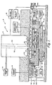
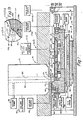
- Ein Teilchenstrahllithographiesystem (10) zum Bearbeiten eines Werkstücks (14) mit einer Teilchenstrahlquelle und einer Vorrichtung zum Erzeugen und Lenken eines Teilchenstrahls (32) durch eine Öffnung (38) als ein Bearbeitungsstrahl für die Oberfläche des Werkstücks, wobei die Öffnung (38) einen Teil einer Vorrichtung zum Unterhalten lediglich eines Teilbereichs der Oberfläche unter Vakuum bildet, wobei weiter ein x-y-Verschiebetisch (50) und eine Aufspannvorrichtung (100) zum Halten des Werkstücks (14) vorgesehen sind, gekennzeichnet durch eine Plattenvorrichtung (64), die kinematisch auf dem x-y-Verschiebetisch (50) angebracht ist, die unter einem vorbestimmten Abstand von der Öffnung (38) gehalten wird und die die Aufspannvorrichtung (100) trägt, wobei die Aufspannvorrichtung relativ zu der Öffnung (38) unabhängig von der Plattenvorrichtung (64) positionierbar ist,
eine Lückeneinstellvorrichtung (162), die eine Vielzahl von Gasstromdüsen umfaßt, wobei die Lückeneinstellvorrichtung (162) zur Orientierung und Positionierung des Werkstücks (14) und der Aufspannvorrichtung (100) relativ zu der Öffnung (38) dient, und
durch eine Arretiervorrichtung (114), die die Aufspannvorrichtung (100) in der Plattenvorrichtung (64) arretiert, nachdem sie durch die Lückeneinstellvorrichtung (162) orientiert und positioniert wurde,
wobei, wenn das Werkstück (14) und die Aufspannvorrichtung in der Plattenvorrichtung (64) orientiert und positioniert sind, die Plattenvorrichtung (64) und der x-y-Verschiebetisch (50) andauernd relativ zu der Öffnung (38) derart gehalten werden, so daß der Raum zwischen der Werkstückoberfläche und der Öffnung (38) konstant ist, unabhängig von der Position des x-y-Verschiebetisches (50). - Das System nach Anspruch 1, wobei die Plattenvorrichtung (64) und der x-y-Verschiebetisch (50) unter dem vorbestimmten Abstand von der Öffnung durch Gaslager (90) gehalten werden.
- Das System nch Anspruch 2, wobei die Plattenvorrichtung (64) zu einer Seite des Teilchenstrahls (32) und der Öffnung (38) zu einer Lade-/Entladeposition verschiebbar ist, wo ein Werkstück auf die Aufspannvorrichtung (100) geladen und entladen werden kann.
- Das System nach Anspruch 3, wobei die Luftlager (90) die Plattenvorrichtung (100) und den x-y-Verschiebetisch (50) relativ zu der Öffnung (38) in der Lade-/Entladeposition halten.
- Das System nach Anspruch 4, wobei die Lückeneinstellvorrichtung (162) in der Lade-/Entladeposition über dem Werkstück (14) gelegen ist, so daß das Werkstück (14) und die Aufspannvorrichtung (100) orientiert und positioniert werden und passend sind, um unter dem Strahl bewegt zu werden, wo der Strahl das Werkstück bearbeitet.
- Ein Verfahren zum Orientieren einer Werkstückoberfläche in einem Teilchenstrahllithographiesystem nach Anspruch 1, in welchem der Teilchenstrahl (32) durch eine Öffnung (38) unter Vakuum auf einen Teilbereich der Oberfläche in der Nähe der Öffnung gelenkt wird, mit den folgenden Schritten:
Bewegen einer Plattenvorrichtung (64) seitlich zu einer Seite der Öffnung, während die Plattenvorrichtung kontinuierlich relativ zu der Öffnung durch Gaslagervorrichtungen (90) orientiert ist,
Anbringen eines Werkstücks (14) auf einer Aufspannvorrichtung (100) in der Plattenvorrichtung und Auftreffenlassen eines Gases aus einer Lückeneinstellvorrichtung (162) auf dem Werkstück, um das Werkstück und die Aufspannvorrichtung relativ zu der Plattenvorrichtung (64) bezüglich eines vorbestimmten Standards zu orientieren,
Arretieren der Aufspannvorrichtung (100) in der Plattenvorrichtung (64) gemäB der durch die Lückeneinstellvorrichtung (162) bestimmten Orientierung, und
Bewegen des Werkstücks (14) seitlich in die Nähe der Öffnung zum Bearbeiten des Werkstücks gemäß einem vorbestimmten Muster, während die Plattenvorrichtung (64) relativ zu der Öffnung durch die Gaslagervorrichtung (162) gehalten wird.
Applications Claiming Priority (2)
| Application Number | Priority Date | Filing Date | Title |
|---|---|---|---|
| US141812 | 1988-01-11 | ||
| US07/141,812 US4818838A (en) | 1988-01-11 | 1988-01-11 | Apparatus for preselecting and maintaining a fixed gap between a workpiece and a vacuum seal apparatus in particle beam lithography systems |
Publications (3)
| Publication Number | Publication Date |
|---|---|
| EP0324436A2 EP0324436A2 (de) | 1989-07-19 |
| EP0324436A3 EP0324436A3 (en) | 1990-07-04 |
| EP0324436B1 true EP0324436B1 (de) | 1994-11-09 |
Family
ID=22497374
Family Applications (1)
| Application Number | Title | Priority Date | Filing Date |
|---|---|---|---|
| EP89100347A Expired - Lifetime EP0324436B1 (de) | 1988-01-11 | 1989-01-10 | Vorrichtung zum Vorwählen und festhalten einer festen Distanz zwischen einem Werkstück und einem Vakuumgerät in Partikelstrahllithographiesystemen |
Country Status (5)
| Country | Link |
|---|---|
| US (1) | US4818838A (de) |
| EP (1) | EP0324436B1 (de) |
| JP (1) | JP2823576B2 (de) |
| CA (1) | CA1294065C (de) |
| DE (1) | DE68919234T2 (de) |
Families Citing this family (27)
| Publication number | Priority date | Publication date | Assignee | Title |
|---|---|---|---|---|
| US5087815A (en) * | 1989-11-08 | 1992-02-11 | Schultz J Albert | High resolution mass spectrometry of recoiled ions for isotopic and trace elemental analysis |
| US5055680A (en) * | 1990-04-03 | 1991-10-08 | Lk Technologies, Inc. | Scanning tunneling microscope |
| JPH04162422A (ja) * | 1990-10-24 | 1992-06-05 | Fujitsu Ltd | 半導体装置の製造装置 |
| JPH0719554B2 (ja) * | 1993-03-25 | 1995-03-06 | 工業技術院長 | 荷電ビーム装置 |
| US5602619A (en) * | 1993-09-22 | 1997-02-11 | Nikon Precision, Inc. | Scanner for step and scan lithography system |
| US5644137A (en) * | 1996-03-04 | 1997-07-01 | Waggener; Herbert A. | Stabilizing support mechanism for electron beam apparatus |
| US5973764A (en) * | 1997-06-19 | 1999-10-26 | Svg Lithography Systems, Inc. | Vacuum assisted debris removal system |
| JP4354039B2 (ja) * | 1999-04-02 | 2009-10-28 | 東京エレクトロン株式会社 | 駆動装置 |
| US6323494B1 (en) | 1999-04-09 | 2001-11-27 | Nikon Corporation | Vertical direction force transducer |
| US6287004B1 (en) | 1999-11-22 | 2001-09-11 | Nikon Corporation | Fluid bearing operable in a vacuum region |
| JP2001242300A (ja) | 2000-03-02 | 2001-09-07 | Sony Corp | 電子ビーム照射装置 |
| TW509823B (en) | 2000-04-17 | 2002-11-11 | Asml Netherlands Bv | Lithographic apparatus, device manufacturing method, and device manufactured thereby |
| US6882899B2 (en) * | 2000-05-16 | 2005-04-19 | Photon Dynamics, Inc. | Sensing head positioning system using two-stage offset air bearings |
| US6473161B2 (en) * | 2000-06-02 | 2002-10-29 | Asml Netherlands B.V. | Lithographic projection apparatus, supporting assembly and device manufacturing method |
| JP2002175770A (ja) | 2000-12-08 | 2002-06-21 | Hitachi Ltd | 気体排気用試料室及びそれを用いた回路パターン形成装置 |
| US6746566B1 (en) | 2001-12-11 | 2004-06-08 | Kla-Tencor Technologies Corporation | Transverse magnetic field voltage isolator |
| US6710354B1 (en) | 2001-12-11 | 2004-03-23 | Kla-Tencor Corporation | Scanning electron microscope architecture and related material handling system |
| US7270735B2 (en) * | 2003-01-21 | 2007-09-18 | Seagate Technology Llc | System and method for holding and releasing a workpiece for electrochemical machining |
| US7394339B1 (en) | 2004-06-30 | 2008-07-01 | Kla-Tencor Technologies Corporation | Transverse magnetic field voltage isolator |
| NL1026547C2 (nl) * | 2004-07-01 | 2006-01-03 | Fei Co | Apparaat voor het evacueren van een sample. |
| JP5033873B2 (ja) * | 2006-06-07 | 2012-09-26 | エフ イー アイ カンパニ | 真空チャンバを有する機器とともに使用されるスライダベアリング |
| CN101461026B (zh) * | 2006-06-07 | 2012-01-18 | Fei公司 | 与包含真空室的装置一起使用的滑动轴承 |
| US7550744B1 (en) | 2007-03-23 | 2009-06-23 | Kla-Tencor Corporation | Chamberless substrate handling |
| US8749753B2 (en) * | 2007-04-27 | 2014-06-10 | Nikon Corporation | Movable body apparatus, exposure apparatus and optical system unit, and device manufacturing method |
| FR2979684B1 (fr) * | 2011-09-07 | 2014-08-08 | Commissariat Energie Atomique | Dispositif de deplacement relatif de deux pieces sous pression differentielle |
| NL2014134B1 (en) * | 2015-01-14 | 2017-01-04 | Smit Thermal Solutions B V | Atomic Layer Deposition apparatus. |
| JP7042071B2 (ja) | 2016-12-20 | 2022-03-25 | エフ・イ-・アイ・カンパニー | eビーム操作用の局部的に排気された容積を用いる集積回路解析システムおよび方法 |
Family Cites Families (4)
| Publication number | Priority date | Publication date | Assignee | Title |
|---|---|---|---|---|
| US4607167A (en) * | 1982-10-19 | 1986-08-19 | Varian Associates, Inc. | Charged particle beam lithography machine incorporating localized vacuum envelope |
| EP0106510B1 (de) * | 1982-10-19 | 1991-11-13 | Varian Associates, Inc. | Bearbeitungsgerät mit einer Vorrichtung zur Erzeugung eines lokalisierten Vakuums |
| US4584479A (en) * | 1982-10-19 | 1986-04-22 | Varian Associates, Inc. | Envelope apparatus for localized vacuum processing |
| US4560880A (en) * | 1983-09-19 | 1985-12-24 | Varian Associates, Inc. | Apparatus for positioning a workpiece in a localized vacuum processing system |
-
1988
- 1988-01-11 US US07/141,812 patent/US4818838A/en not_active Expired - Lifetime
-
1989
- 1989-01-10 EP EP89100347A patent/EP0324436B1/de not_active Expired - Lifetime
- 1989-01-10 DE DE68919234T patent/DE68919234T2/de not_active Expired - Fee Related
- 1989-01-11 CA CA000587987A patent/CA1294065C/en not_active Expired - Lifetime
- 1989-01-11 JP JP1002981A patent/JP2823576B2/ja not_active Expired - Fee Related
Also Published As
| Publication number | Publication date |
|---|---|
| CA1294065C (en) | 1992-01-07 |
| EP0324436A2 (de) | 1989-07-19 |
| EP0324436A3 (en) | 1990-07-04 |
| JPH023219A (ja) | 1990-01-08 |
| US4818838A (en) | 1989-04-04 |
| JP2823576B2 (ja) | 1998-11-11 |
| DE68919234T2 (de) | 1995-03-23 |
| DE68919234D1 (de) | 1994-12-15 |
Similar Documents
| Publication | Publication Date | Title |
|---|---|---|
| EP0324436B1 (de) | Vorrichtung zum Vorwählen und festhalten einer festen Distanz zwischen einem Werkstück und einem Vakuumgerät in Partikelstrahllithographiesystemen | |
| US6214692B1 (en) | Method and apparatus for the aligned joining of disk-shaped semiconductor substrates | |
| JPS5993249A (ja) | 局部的真空処理のための間隙制御装置 | |
| US5197089A (en) | Pin chuck for lithography system | |
| KR101366754B1 (ko) | 고속의 기판 정렬기 장치 | |
| KR102126693B1 (ko) | 얼라인먼트 장치, 반도체 웨이퍼 처리장치 및 얼라인먼트 방법 | |
| US7783377B2 (en) | Substrate loading and unloading apparatus | |
| EP0361934B1 (de) | Belichtungsverfahren | |
| US4598242A (en) | Mask feed method and apparatus for exposure replicate systems | |
| JPH1041376A (ja) | 基板保持装置、基板保持方法及び露光装置 | |
| US4648708A (en) | Pattern transfer apparatus | |
| JPH0323631B2 (de) | ||
| JP3340151B2 (ja) | ウエハー載置装置 | |
| JPS5990926A (ja) | 局部的真空エンベロプを組み込んだ荷電粒子ビ−ムリソグラフイ装置 | |
| JPH07231028A (ja) | 搬送装置および搬送方法 | |
| JPH05304071A (ja) | 露光装置のステージ | |
| JPH08288337A (ja) | チップボンディング方法及びその装置 | |
| JPH0462951A (ja) | ウエハ移し換え装置 | |
| US11975422B2 (en) | Minimal contact gripping of thin optical devices | |
| JP3371164B2 (ja) | 枚葉処理式イオン注入装置 | |
| JPH0564452B2 (de) | ||
| JPH07142348A (ja) | 露光装置 | |
| CN116169032A (zh) | 接合装置和接合方法 | |
| JPH06151271A (ja) | 露光装置 | |
| KR20000014177A (ko) | 웨이퍼 이송장치 |
Legal Events
| Date | Code | Title | Description |
|---|---|---|---|
| PUAI | Public reference made under article 153(3) epc to a published international application that has entered the european phase |
Free format text: ORIGINAL CODE: 0009012 |
|
| AK | Designated contracting states |
Kind code of ref document: A2 Designated state(s): DE FR GB IT NL |
|
| PUAL | Search report despatched |
Free format text: ORIGINAL CODE: 0009013 |
|
| AK | Designated contracting states |
Kind code of ref document: A3 Designated state(s): DE FR GB IT NL |
|
| RAP1 | Party data changed (applicant data changed or rights of an application transferred) |
Owner name: ETEC SYSTEMS, INC. |
|
| 17P | Request for examination filed |
Effective date: 19910102 |
|
| 17Q | First examination report despatched |
Effective date: 19930312 |
|
| GRAA | (expected) grant |
Free format text: ORIGINAL CODE: 0009210 |
|
| AK | Designated contracting states |
Kind code of ref document: B1 Designated state(s): DE FR GB IT NL |
|
| REF | Corresponds to: |
Ref document number: 68919234 Country of ref document: DE Date of ref document: 19941215 |
|
| ITF | It: translation for a ep patent filed |
Owner name: STUDIO GLP S.R.L. |
|
| ET | Fr: translation filed | ||
| PLBE | No opposition filed within time limit |
Free format text: ORIGINAL CODE: 0009261 |
|
| STAA | Information on the status of an ep patent application or granted ep patent |
Free format text: STATUS: NO OPPOSITION FILED WITHIN TIME LIMIT |
|
| 26N | No opposition filed | ||
| PGFP | Annual fee paid to national office [announced via postgrant information from national office to epo] |
Ref country code: FR Payment date: 19990118 Year of fee payment: 11 |
|
| PG25 | Lapsed in a contracting state [announced via postgrant information from national office to epo] |
Ref country code: FR Free format text: LAPSE BECAUSE OF NON-PAYMENT OF DUE FEES Effective date: 20000929 |
|
| REG | Reference to a national code |
Ref country code: FR Ref legal event code: ST |
|
| REG | Reference to a national code |
Ref country code: GB Ref legal event code: IF02 |
|
| PGFP | Annual fee paid to national office [announced via postgrant information from national office to epo] |
Ref country code: GB Payment date: 20020129 Year of fee payment: 14 |
|
| PGFP | Annual fee paid to national office [announced via postgrant information from national office to epo] |
Ref country code: DE Payment date: 20020228 Year of fee payment: 14 |
|
| PGFP | Annual fee paid to national office [announced via postgrant information from national office to epo] |
Ref country code: NL Payment date: 20020425 Year of fee payment: 14 |
|
| PG25 | Lapsed in a contracting state [announced via postgrant information from national office to epo] |
Ref country code: GB Free format text: LAPSE BECAUSE OF NON-PAYMENT OF DUE FEES Effective date: 20030110 |
|
| REG | Reference to a national code |
Ref country code: GB Ref legal event code: 732E |
|
| NLS | Nl: assignments of ep-patents |
Owner name: APPLIED MATERIALS, INC |
|
| PG25 | Lapsed in a contracting state [announced via postgrant information from national office to epo] |
Ref country code: NL Free format text: LAPSE BECAUSE OF NON-PAYMENT OF DUE FEES Effective date: 20030801 Ref country code: DE Free format text: LAPSE BECAUSE OF NON-PAYMENT OF DUE FEES Effective date: 20030801 |
|
| GBPC | Gb: european patent ceased through non-payment of renewal fee |
Effective date: 20030110 |
|
| NLV4 | Nl: lapsed or anulled due to non-payment of the annual fee |
Effective date: 20030801 |
|
| PG25 | Lapsed in a contracting state [announced via postgrant information from national office to epo] |
Ref country code: IT Free format text: LAPSE BECAUSE OF NON-PAYMENT OF DUE FEES Effective date: 20050110 |