EP0324436B1 - Apparatus for preselecting and maintaining a fixed gap between a workpiece and a vacuum seal apparatus in particle beam lithography systems - Google Patents
Apparatus for preselecting and maintaining a fixed gap between a workpiece and a vacuum seal apparatus in particle beam lithography systems Download PDFInfo
- Publication number
- EP0324436B1 EP0324436B1 EP89100347A EP89100347A EP0324436B1 EP 0324436 B1 EP0324436 B1 EP 0324436B1 EP 89100347 A EP89100347 A EP 89100347A EP 89100347 A EP89100347 A EP 89100347A EP 0324436 B1 EP0324436 B1 EP 0324436B1
- Authority
- EP
- European Patent Office
- Prior art keywords
- workpiece
- chuck
- aperture
- particle beam
- stage
- Prior art date
- Legal status (The legal status is an assumption and is not a legal conclusion. Google has not performed a legal analysis and makes no representation as to the accuracy of the status listed.)
- Expired - Lifetime
Links
Images


Classifications
-
- H—ELECTRICITY
- H01—ELECTRIC ELEMENTS
- H01J—ELECTRIC DISCHARGE TUBES OR DISCHARGE LAMPS
- H01J37/00—Discharge tubes with provision for introducing objects or material to be exposed to the discharge, e.g. for the purpose of examination or processing thereof
- H01J37/30—Electron-beam or ion-beam tubes for localised treatment of objects
- H01J37/301—Arrangements enabling beams to pass between regions of different pressure
-
- H—ELECTRICITY
- H01—ELECTRIC ELEMENTS
- H01L—SEMICONDUCTOR DEVICES NOT COVERED BY CLASS H10
- H01L21/00—Processes or apparatus adapted for the manufacture or treatment of semiconductor or solid state devices or of parts thereof
- H01L21/67—Apparatus specially adapted for handling semiconductor or electric solid state devices during manufacture or treatment thereof; Apparatus specially adapted for handling wafers during manufacture or treatment of semiconductor or electric solid state devices or components ; Apparatus not specifically provided for elsewhere
- H01L21/677—Apparatus specially adapted for handling semiconductor or electric solid state devices during manufacture or treatment thereof; Apparatus specially adapted for handling wafers during manufacture or treatment of semiconductor or electric solid state devices or components ; Apparatus not specifically provided for elsewhere for conveying, e.g. between different workstations
- H01L21/67763—Apparatus specially adapted for handling semiconductor or electric solid state devices during manufacture or treatment thereof; Apparatus specially adapted for handling wafers during manufacture or treatment of semiconductor or electric solid state devices or components ; Apparatus not specifically provided for elsewhere for conveying, e.g. between different workstations the wafers being stored in a carrier, involving loading and unloading
- H01L21/67778—Apparatus specially adapted for handling semiconductor or electric solid state devices during manufacture or treatment thereof; Apparatus specially adapted for handling wafers during manufacture or treatment of semiconductor or electric solid state devices or components ; Apparatus not specifically provided for elsewhere for conveying, e.g. between different workstations the wafers being stored in a carrier, involving loading and unloading involving loading and unloading of wafers
Landscapes
- Engineering & Computer Science (AREA)
- Manufacturing & Machinery (AREA)
- Physics & Mathematics (AREA)
- Analytical Chemistry (AREA)
- Condensed Matter Physics & Semiconductors (AREA)
- General Physics & Mathematics (AREA)
- Chemical & Material Sciences (AREA)
- Computer Hardware Design (AREA)
- Microelectronics & Electronic Packaging (AREA)
- Power Engineering (AREA)
- Exposure And Positioning Against Photoresist Photosensitive Materials (AREA)
- Container, Conveyance, Adherence, Positioning, Of Wafer (AREA)
- Electron Beam Exposure (AREA)
Description
- The following applications are related:
European Application No. EP-A-0 295 616 of L. Young entitled "Differentially Pumped Seal Apparatus" and - European Application No. EP-A-0 312 066 of L. Young and G. Howard entitled "A Guard Ring for a Differentially Pumped Seal Apparatus". These applications will be discussed layer.
- This invention relates to a particle beam lithography system as described in the first part of
claim 1 for processing a workpiece, such as a semiconductor wafer or mask. - The invention relates also to a method of orientating a workpiece surface in a particle beam lithography system according to
claim 1. - Such a system is known from European Patent Application EP-
A-0 106 510 which discloses a particle beam lithography system comprising a particle beam column including a particle source and means to direct particle beams through the column to an aperture of a graded vacuum seal between said column and a workpiece, and further comprising a workpiece holding system comprising an x-y-stage and a chuck supported on the x-y-stage through actuators capable of moving said chuck in a Z-direction and responsive to a signal obtained via an electronic feedback circuit from a gap sensing means. - U.S. Patent No. US-A-4 524 261 to Petric et al entitled "Localized Vacuum Processing Apparatus (hereinafter referred to as the ′261 patent), discloses a localized vacuum seal apparatus, hereinafter called simply a seal apparatus, which provides a non-contacting graded vacuum seal between the seal apparatus and a workpiece to achieve a relatively high vacuum zone in close proximity to the beam of a particle beam lithography system while the remainder of the workpiece remained at ambient pressure as the workpiece is moved in an X-Y direction for processing the entire workpiece. The space between the tip of the seal apparatus and the surface of the workpiece is referred to as a gap.
- The European Patent Application EP-A-0 295 616 discloses and claims an improvement over the seal apparatus of the ′261 patent in that the Young seal apparatus obtains higher vacuum and a smaller gap between the seal apparatus and the workpiece.
- The European Patent Application EP-A-0 312 066 discloses and claims a guard ring of pressurized gas surrounding the seal apparatus to reduce the possibility of contamination coming in contact with the workpiece surface and entering the beam column.
- U.S. Patent No. US-A-4 528 451 to Petric et al entitled "Gap Control System for Localized Vacuum Processing" (hereinafter referred to as the ′451 patent), it was felt necessary to dynamically control the size of the gap during workpiece processing and thus apparatus for sensing and controlling the gap is disclosed. Specifically, a capacitor sensing device is used to sense the size of the gap and feed this information back to a control and drive mechanism to vary the vertical direction (Z axis) of the workpiece relative to the seal apparatus. The sensing and control is a continuous operation and the gap size is varied within a selected range during workpiece processing. It is an object of the present invention to provide an improved particle beam lithography system.
- This object is solved according to the invention with the particle beam lithography system according to
claim 1 and the method of orientating a workpiece surface in such a particle beam lithography system according to claim 6. - This invention improves this prior art as disclosed in the ′451 patent by providing a means by which a workpiece is held at a predetermined gap size during the processing of the workpiece. This overcomes problems involved in dynamically controlling a variable gap and eliminates the gap size sensors and feedback and drive mechanisms.
- According to the present invention, at a workpiece loading and unloading position, to one side of the beam and beam column of a particle beam lithography system, a workpiece to be processed, is placed on a vacuum chuck to eliminate any irregularity or warpage of the workpiece. At this same position, the workpiece is oriented by gap setting means and fixed at a preselected distance from a standard. This distance correlates with a preselected gap size. The workpiece and chuck are then moved beneath the seal apparatus and beam column for workpiece processing. After processing, the workpiece and chuck are returned to the loading/unloading position to be removed from the lithography system. An interface plate, holding the workpiece and chuck, is maintained in a precise fixed relationship with the standard and the seal apparatus by gas bearings during workpiece processing as well as during loading and unloading of the workpiece. This also maintains the gap at a fixed size during workpiece processing. The interface plate is moved to and from the loading/unloading position to the workpiece processing position by an X-Y stage and a workpiece transport system is provided to transport the workpieces to and from the lithography system and to and from appropriate workpiece cassettes.
- From the foregoing, it can be seen that a primary object of this invention is to improve a particle beam lithography system by providing the system with a fixed gap technique thus simplifying the X-Y stage mechanical hardware as well as the system electronics and software.
- Still another object of this invention is to improve a particle beam lithography system by the use of gas bearings to position the X-Y stage during workpiece loading/unloading and processing.
- Still another object is to improve a particle beam lithography system by providing a means by which a workpiece is positioned relative to a standard by gap setting means so that there is a preselected fixed gap between a seal apparatus and the workpiece during processing by the particle beam.
- Still another object of this invention is to provide an improved method and apparatus of loading and unloading a workpiece for processing in a particle beam lithography system.
- These and other objects of the invention will be apparent to those skilled in the art after having studied the accompanying drawings and the detailed description hereinafter.
- Figure 1 is a schematic illustration of a particle beam lithography system incorporating apparatus of the present invention and illustrates the workpiece in a position to be treated by the particle beam.
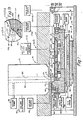
- Figure 2 is a schematic illustration, like Figure 1, but illustrating the workpiece in a loading/unloading position to be precisely oriented and fixed relative to a standard by gap setting means; one version of the gap setting means being shown in this figure,
- Figure 3 is a partial illustration of a chuck, an interface plate and of one type of clamping means,
- Figure 4 is a plan view of the particle beam lithography system showing the position of the workpiece and beam column when the workpiece is in the loading/unloading position, showing apparatus for transporting a workpiece to and from the particle beam lithography system, and also showing the gap setting means of figure 2,
- Figures 5a-5g are partial cross-sectional schematic views showing the steps involved in loading, unloading and orienting a workpiece relative to the interface plate,
- Figure 6 is an illustration of axes definitions as used herein,
- Figure 7 is a schematic illustration, like figure 2, showing the workpiece in the loading/unloading position, but showing another version of the gap setting means, and
- Figure 8 is a partial plan view of the chuck and workpiece showing the gas jets arranged in a triangle in this latter version of the gap setting means.
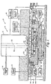
- To enable a clear understanding of the drawings and description herein at the outset, it is pointed out that there are essentially two parts to the disclosed particle beam lithography system of this invention, identified in its entirety as 10. These two parts are called a stationary beam part and a movable work holding part, simply for identification and denoted, respectively, as B and W. The stationary beam part B includes a
particle beam column 12 and its associated apparatus, and the movable workholding part W includes apparatus on which theworkpiece 14 is loaded, processed and unloaded. Theworkpiece 14 is a semiconductor wafer or mask and is referred to as a substrate or simply a wafer. - The beam part B, in addition to the
beam column 12, includes aseal apparatus 16 located at the output of thebeam column 12 and may also include aguard ring 20, shown as arrows, surrounding theseal apparatus 16 and connected to apressure pump 22. Theseal apparatus 16 andguard ring 20 are formed in alarge plate 24, called a manifold, on which thebeam column 12 is mounted. Themanifold 24 is supported on abase 26 by posts 30 (only one shown in figure 1) and thus is stationary and at a fixed distance from thebase 26. - The
beam column 12 includes an electron or ionized particle source, demagnification optics and projection and deflection optics which generate a finely focusedbeam 32 and may also include illumination and shaping optics when a shaped beam is utilized. A central tube 34 (shown in phantom) is within thecolumn 12 and is traversed by thebeam 32 and maintained at a high vacuum by ahigh vacuum pump 36 coupled to thecolumn 12. Thebeam 32 passes through anaperture 38 in theseal apparatus 16 and impinges on theworkpiece 14. Thecomplete lithography system 10 further includes a computer (controller) and associated electronics which controls the beam, the drive system, the vacuum system, the workholding system and stores pattern data and provides beam control signals; all identified by a block diagram 40. - The
seal apparatus 16 includes a plurality of conically shaped sleeves forming concentric apertures (one shown as the central aperture 38) which terminate in a generallyplanar tip 42 positioned, during processing, a distance slightly above theworkpiece 14, which distance is the aforementioned gap, identified as G, and is important to the operation of theseal apparatus 16 and the graded seal obtained thereby. The apertures are coupled to first, second and third stage pumps, identified only as a block diagram 44, which gradually reduce the pressure from ambient to a high vacuum level at thecentral aperture 38 corresponding to the vacuum in thecentral tube 34. Thebeam 32 is scanned over the region of the workpiece within thecentral aperture 38 as theworkpiece 14 moves horizontally relative to theseal apparatus 16 while the remainder of theworkpiece 14 is at ambient pressure. - The
seal apparatus 16 which accomplishes a better reduction in vacuum and a smaller gap size, ie, about 10 to 15 microns, than that of the prior art seal apparatus of the ′261 patent is the preferred seal apparatus to be used and, if more detailed information concerning the preferred seal apparatus is necessary, reference is made to the Young application, supra. - Since air at ambient pressure is reduced to a high vacuum level at the
central aperture 38, there is a possibility of contaminants in the atmosphere and/or on theworkpiece 14 being sucked into the central aperture andbeam column 12. To reduce, or avoid this possibility, theguard ring 20 is preferably incorporated into the particlebeam lithography system 10. Thisguard ring 20 is a ring of pressurized gas surrounding theseal apparatus 16 and impinging on theworkpiece 14 and may be filtered dry air or gas, or an inert or ionized gas; all of which may be preheated. If more detailed information concerning thisguard ring 20 is necessary, reference is made to the Young and Howard application, supra. - The workholding movable part W of the particle beam lithography system includes a
conventional X-Y stage 50 with astationary plate 52 supported on thebase 26 by levelingjacks 54 which are used to initially level theX-Y stage 50 relative to themanifold 24. TheX-Y stage 50 is driven in the X-Y direction by a conventional X-Y drive, identified by the block diagram 62. - An
interface plate 64, movable by the X-Y stage, is supported on the top of thestage 50 by akinematic mount 66 normally stiff in the X,Y, and ϑ direction, but soft and biased in the Z direction. Figure 6 illustrates the axes definitions as mentioned above. - The
interface plate 64 is provided with threegas bearing pads 70 which extend above thetop surface 72 of theinterface plate 64 and are triangulated, as more clearly shown in figure 4, to stabilize theinterface plate 64 relative to the bottom 74 of the manifold 24. As also shown in figure 4, eachpad 70 has a plurality ofports 76, shown arranged in a circle, for pressurized gas and acentral port 80 for a vacuum return. Other arrangements of theports Gas ports 76 and vacuum returnports 80 are connected, viainner channels arrows 90 between the manifold bottom 74 and eachpad 70 thereby spacing thepads 70 at a predetermined distance of about 2 to 3 microns from themanifold bottom 74. This film of gas continually reacts against thekinematic mount 66. - The
interface plate 64 is also provided withmirrors 92 forming part of a position sensing system, identified by block diagrams 94, which are conventionally interferometers, to sense a position of theinterface plate 64 and theX-Y stage 50 and feedback position information to theX-Y drive 50 under the control of the lithography system electronics. - The
interface plate 64 has acentral recess 96 in which avacuum chuck 100 is supported bysoft springs 102 biased in the Z direction. Thevacuum chuck 100 is connected to avacuum pump 104 to provide the vacuum for holding the workpiece flat against the chuck surface to eliminate any irregularity or warpage in theworkpiece 14.Chuck 100 has an inner vacuum chamber (not shown) for connecting thevacuum pump 104 to a plurality ofapertures 106 formed in the top of thechuck 100, as shown in figure 4, where a portion of aworkpiece 14 is broken away. Also shown in this figure, and in the other figures, are three centrally locatedlifters 110 arranged in a triangle to assist in loading and unloading theworkpiece 14 on thevacuum chuck 100. Thischuck 100 is conventional and is used in other workpiece processing systems. - The
interface plate 64 also contains a fiducial cup andgrid 112, and a plurality of clamping means 114, shown as arrows in figures 1 and 2, to fix thechuck 100 and theworkpiece 14 at the desired position, preferably as coplanar as possible to thetop surface 72 of theinterface plate 64. - Figure 3 illustrates one embodiment of the clamping means 114. The
chuck 100 is provided with a plurality of radially outwardly extending tabs 116 (only one shown) which extend into slots 120 in theinterface plate 64 where suitable clamps, such aspins 122, will engage or disengage thetabs 116 to clamp or release thechuck 100 at the appropriate time. As shown, one side of thetab 116 touches one side of the slot 120 to minimize the motion imparted to the chuck by the clamping action. Ideally, the clamping action should impart no motion to the chuck. - Figure 1 illustrates the
workpiece 14 in position to be processed by thebeam 32 as theworkpiece 14 is translated in the X-Y direction beneath thebeam 32 by theX-Y stage 50 in the conventional manner. - As mentioned above, in this system, the
gas bearing films 90 maintain thepads 70 at the predetermined distance from the manifold bottom 74 and, in turn, maintain theworkpiece 14 at a predetermined fixed distance (gap G) from theplanar tip 42 of theseal apparatus 16. This gap G, being fixed at a preselected size during workpiece processing, distinguishes this invention from the prior art variable gap system as shown in the ′451 patent. - As shown in figures 2 and 4, the
interface plate 64 has been moved to one side of thebeam column 12 by theX-Y stage 50 so that the fiducial cup andgrid 112 are directly beneath theparticle beam 32 in its neutral position and, of course, thegas bearing films 90 continue to maintain theinterface plate 64 at the predetermined distance from themanifold bottom 74. This is the workpiece loading/unloading position and is shown to be at the right of thebeam column 12 in figure 2 and below thebeam column 12 in figure 4. - Figure 4 shows two
vacuum wands workpiece transport system 130.Wand 124 is shown in two positions; one extending into acassette 132 and the other extending over thevacuum chuck 100 and beneath theworkpiece 14 simply to show how the wands operate.Wand 124 transportsunprocessed workpieces 14 to thelithography system 10 from acassette 132, shown to the left of the lithography system in figure 4, while theother wand 126 transports the processed workpieces from the lithography system to thecassette 134 shown to the right of the lithography system. As can also be seen in figure 4, thetransport system 130 includes air bars 136 and 140 on which thewands arrows 142. Suitable means, such as magnet and coil assemblies (not shown) inside thebars air pressure pump 150 to provide the necessary air under pressure to form air bearings for sliding movement of the wands. Thewands vacuum pump 152 to provide the necessary vacuum for lifting and carryingworkpieces 14 to and from thecassettes Wands arrows 154. In practice, the air bars 136 and 140 would be positioned further from thelithography system 10 than shown for proper clearance of the wands andair bearing pads 70. The position shown in figure 4 was dictated by drawing size constraints. Also, other variations of the wands are possible, for example, the workpiece lifting portion of the wands may also be capable of rotating horizontally to position the workpieces on the chuck and remove the same after processing. - Thus, during operation of the
workpiece transport system 130, by suitable activation of the vacuum inwand 124, anunprocessed workpiece 14 is removed fromcassette 132 and placed on a prealigner 160 where the unprocessed workpiece is oriented in the ϑ direction and its center determined for later positioning on thevacuum chuck 100. Reference is made to the U.S. Patent of Quinn No. US-A-4 425 075 entitled "Wafer Aligner" as an example of workpiece aligners. This patent also shows vacuum arms for lifting and positioning the workpieces. - After orientation, the
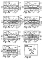
wand 124 is again activated to lift the oriented unprocessed workpiece and move it over thechuck 100 as shown in figure 4. If a processed workpiece had been on thechuck 100, it would have been removed by thewand 126 and placed in thecassette 134. - Figures 5a-5g show the steps involved in unloading and loading and orienting the
workpiece 14 relative to the bottom of the manifold bottom 74 to preselect and fix the gap size. Figure 4 should also be considered a connection with the steps of figure 5a-5g since the latter are done when theinterface plate 64 is in the loading/unloading position of figure 4. - Figure 5a shows the
vacuum chuck 100 without aworkpiece 14 and with clamping means 114 disengaged as represented by the arrows spaced from the chuck. Thechuck 100 is in its uppermost position and a chuck retracting means 156 is shown schematically activated by being in contact with the bottom of the chuck. At this time, the vacuum to thechuck 100 is turned off. The chuck retracting means 156 may take any suitable form. A hook, releasably connectable to the bottom of the chuck and to a motor means (block diagram 160 in figures 1 and 2) which move the chuck rapidly, is one suitable form of such a device. - Figure 5b shows the next step prior to loading an
unprocessed workpiece 14 onto thechuck 100. The clamping means 114 is still disengaged, allowing the chuck retracting means 156 to lower the chuck against thesprings 102 so that there is sufficient space beneath the manifold bottom 74 to allow thewand 124 to position a workpiece on the chuck. The chuck retracting means 156 is still engaged to thechuck 100 but shown shorter to schematically illustrate its operation. The vacuum to the chuck is still turned off. - Figure 5c shows the
wand 124 and itsworkpiece 14 positioned over thechuck 100 with the chuck still in its lowermost position and the clamping means 114 still disengaged. - Figure 5d shows the
lifters 110 raised to engage the under surface of the workpiece. When this step takes place, thewand 124 is removed. Thechuck 100 is still in its lowermost position and the clamping means 114 is still disengaged. - Figure 5e shows the workpiece resting on the top of the
vacuum chuck 100 by the retraction of thelifters 110. The vacuum chuck is still in its lowermost position and the clamping means 114 still disengaged. At this time, the vacuum to the vacuum chuck will be turned on to hold the workpiece flat on the chuck. - Figure 5f shows the workpiece and vacuum chuck raised but the clamping means 114 still disengaged. The chuck retracting means 156 was disengaged, as schematically represented by the disconnection thereof from the chuck, allowing the
springs 102 to raise the chuck to the position shown. At this time, a gap setting means 162 is activated. Figures 2 and 4 show the preferred version of the gap setting means 162. This gap setting means 162 comprises a plurality of gas jets represented byarrows 164 impinging on the workpiece from a plurality of passages 166 (only one shown in figure 2) which are connected to a source ofpressurized gas 170. Thesepassages 164 are shown arranged in a circle in figure 4 as one example of their arrangement. This orients the workpiece at a fixed gap parallel to the standard (manifold bottom 74). - Finally, with the workpiece and chuck properly oriented and spaced, the clamping means 114 is activated to engage and hold the chuck and workpiece in position as represented by the arrows touching the chuck. The gas to the gas jets is turned off.
- Next, the
interface plate 64 will be moved beneath thebeam column 12 for workpiece processing in a conventional manner. - As mentioned above, figures 2 and 4 show the preferred embodiment of this invention in which the gap setting means 162 creates a gas film between the manifold bottom 74 and the workpiece thereby spacing the workpiece from the manifold bottom by a predetermined amount. The film is schematically represented by the horizontal component arrows 164a. A suitable sensor, such as an optical sensor, represented by block diagram 172 and arrow 174, is then activated to determine if the spacing between the manifold bottom and the workpiece is correct. If the spacing is correct, the
interface plate 64 will then be transported beneath the beam column for processing the workpiece as stated above. On the other hand, if the signal from the sensor, as represented by block diagram 172 and arrow 174, indicates that the spacing is not correct, the clamping means 114 are disengaged and the process of orienting the workpiece by the gap setting means is repeated until the spacing is correct. After the correct spacing is achieved and the chuck is clamped, the pressurized gas is turned off. - Figures 7 and 8 show another embodiment of this invention wherein the gap setting means 162b (the second version of the gap setting means) comprises three height gauge gas jets 164b which direct pressurized gas onto
workpiece 14. Theworkpiece 14 is moved in the Z direction by piezoelectric drive means 102b which provide a fine Z adjustment. These gas jets 164b are arranged in a triangle and are connected to a gas pressure source 170b through passages 166b. These gas jets 164b and fine Z adjustment means 102b function similar to the gas jets and fine Z adjustment means in other semiconductor aligning devices and are provided with pneumatic, optical or capacitative type sensing devices, denoted as block diagram 172b and arrow 174b, which determine the correct spacing between the workpiece 14 and the manifold 24. - Since this type of gas jets 164b require more space between the manifold 24 and the
workpiece 14, the bottom of the manifold 24 is provided with a cut-away portion by an amount shown byledge 180. To distinguish this manifold bottom from themanifold bottom 74 of the prior embodiment, this manifold bottom, as cut-away, which is also a standard as in the prior embodiment, is denoted as 74b. However, the concept of fixing and maintaining the gap G is the same as in the prior embodiment since the depth of the cut-away portion is a known quantity relative to the workpiece. - During the loading process only, the sensors, as represented by the block diagram 172b and arrow 174b, are dynamic and monitor the space between the workpiece 14 and the manifold bottom 74b until the
workpiece 14 is correctly positioned, at which time the clamping means 114 are activated as in figures 5f and 5g and the pressurized gas turned off so that theinterference plate 64 may be moved beneath thecolumn 12 where theworkpiece 14 may be processed. - It should be apparent in the embodiments of figures 7 and 8 that those components which have the same functions as in the prior embodiment have been given the same reference numerals and those components which provide similar functions as in the prior embodiments have been given the same reference numerals but with a suffix b. This simplifies and shortens the description of the components in these latter figures. Note that the workpiece is loaded/unloaded within the cut-away portion 74b of the manifold and, in this embodiment, the
wands springs 102, have been eliminated in the embodiment of figures 7 and 8 and, therefore, these components as steps in adjusting the gap G in figures 5a-5g are eliminated but the other steps in establishing the gap in this latter embodiment remain the same.
Claims (6)
- A particle beam lithography system (10) for treating a workpiece (14) including a particle beam source and means for generating and directing a particle beam (32) through an aperture (38) as a treating beam for said workpiece surface, said aperture (38) forming part of a means for maintaining only a portion of the surface of said workpiece in a vacuum, further comprising an x-y-stage (50) and chuck means (100) for holding said workpiece (14), characterised by, plate means (64) kinematically mounted on said x-y-stage (50), maintained at a predetermined distance from said aperture (38) and carrying said chuck means (100) wherein said chuck means is capable of being positioned relative to said aperture (38) independently of said plate means (64),
gap setting means (162) comprising a plurality of gas jets, said gap setting means (162) being operative to orient and position said workpiece (14) and said chuck means (100) relative to said aperture (38), and
locking means (114) locking said chuck means (100) in said plate means (64) after being oriented and positioned by said gap setting means (162),
whereby when said workpiece (14) on said chuck means is oriented and positioned in said plate means (64), said plate means (64) and x-y-stage (50) are continuously maintained relative to said aperture (38) so that the space between said workpiece surface and said aperture (38) is constant regardless of the position of said x-y-stage (50). - The system as claimed in claim 1 wherein said plate means (64) and x-y-stage (50) are maintained at said predetermined distance from said aperture by gas bearings (90).
- The system as claimed in claim 2 wherein said plate means (64) is movable to one side of said particle beam (32) and aperture (38) to a loading/unloading position where a workpiece may be loaded and unloaded from said chuck means (100).
- The system as claimed in claim 3 wherein said air bearings (90) maintain said plate means (64) and said x-y-stage (50) relative to said aperture (38) in said loading/unloading position.
- The system as claimed in claim 4 wherein said gap setting means (162) is located over said workpiece (14) while in the loading/unloading position so that said workpiece (14) and chuck (100) are oriented and positioned and ready to be moved to beneath the beam where said beam treats said workpiece.
- A method of orientating a workpiece surface in a particle beam lithography system according to claim 1 in which the particle beam (32) is directed through an aperture (38) in vacuum on a portion of said surface approximate said aperture comprising the steps of:
moving a plate means (64) laterally to one side of said aperture while said state means is continuously oriented relative to said aperture by gas bearing means (90),
placing a workpiece (14) in a chuck (100) in said plate means and impinging gas from gap setting means (162) on said workpiece to orient said workpiece and chuck relative to said plate means (64) and to a predetermined standard,
locking said chuck (100) in said plate means (64) according to said orientation determined by said gap setting means (162), and
moving said workpiece (14) laterally proximate said aperture for treating said workpiece in accordance with a predetermined pattern while said plate means (64) is maintaned relative to said aperture by said gas bearing means (162).
Applications Claiming Priority (2)
| Application Number | Priority Date | Filing Date | Title |
|---|---|---|---|
| US07/141,812 US4818838A (en) | 1988-01-11 | 1988-01-11 | Apparatus for preselecting and maintaining a fixed gap between a workpiece and a vacuum seal apparatus in particle beam lithography systems |
| US141812 | 1988-01-11 |
Publications (3)
| Publication Number | Publication Date |
|---|---|
| EP0324436A2 EP0324436A2 (en) | 1989-07-19 |
| EP0324436A3 EP0324436A3 (en) | 1990-07-04 |
| EP0324436B1 true EP0324436B1 (en) | 1994-11-09 |
Family
ID=22497374
Family Applications (1)
| Application Number | Title | Priority Date | Filing Date |
|---|---|---|---|
| EP89100347A Expired - Lifetime EP0324436B1 (en) | 1988-01-11 | 1989-01-10 | Apparatus for preselecting and maintaining a fixed gap between a workpiece and a vacuum seal apparatus in particle beam lithography systems |
Country Status (5)
| Country | Link |
|---|---|
| US (1) | US4818838A (en) |
| EP (1) | EP0324436B1 (en) |
| JP (1) | JP2823576B2 (en) |
| CA (1) | CA1294065C (en) |
| DE (1) | DE68919234T2 (en) |
Families Citing this family (27)
| Publication number | Priority date | Publication date | Assignee | Title |
|---|---|---|---|---|
| US5087815A (en) * | 1989-11-08 | 1992-02-11 | Schultz J Albert | High resolution mass spectrometry of recoiled ions for isotopic and trace elemental analysis |
| US5055680A (en) * | 1990-04-03 | 1991-10-08 | Lk Technologies, Inc. | Scanning tunneling microscope |
| JPH04162422A (en) * | 1990-10-24 | 1992-06-05 | Fujitsu Ltd | Production device for semiconductor device |
| JPH0719554B2 (en) * | 1993-03-25 | 1995-03-06 | 工業技術院長 | Charged beam device |
| US5602619A (en) * | 1993-09-22 | 1997-02-11 | Nikon Precision, Inc. | Scanner for step and scan lithography system |
| US5644137A (en) * | 1996-03-04 | 1997-07-01 | Waggener; Herbert A. | Stabilizing support mechanism for electron beam apparatus |
| US5973764A (en) * | 1997-06-19 | 1999-10-26 | Svg Lithography Systems, Inc. | Vacuum assisted debris removal system |
| JP4354039B2 (en) * | 1999-04-02 | 2009-10-28 | 東京エレクトロン株式会社 | Drive device |
| US6323494B1 (en) | 1999-04-09 | 2001-11-27 | Nikon Corporation | Vertical direction force transducer |
| US6287004B1 (en) | 1999-11-22 | 2001-09-11 | Nikon Corporation | Fluid bearing operable in a vacuum region |
| JP2001242300A (en) * | 2000-03-02 | 2001-09-07 | Sony Corp | Electron beam irradiation device |
| TW509823B (en) | 2000-04-17 | 2002-11-11 | Asml Netherlands Bv | Lithographic apparatus, device manufacturing method, and device manufactured thereby |
| US6882899B2 (en) * | 2000-05-16 | 2005-04-19 | Photon Dynamics, Inc. | Sensing head positioning system using two-stage offset air bearings |
| KR100592576B1 (en) * | 2000-06-02 | 2006-06-26 | 에이에스엠엘 네델란즈 비.브이. | Lithographic projection apparatus, supporting assembly and device manufacturing method |
| JP2002175770A (en) | 2000-12-08 | 2002-06-21 | Hitachi Ltd | Sample chamber for gas exhaustion and circuit pattern forming device using the same |
| US6710354B1 (en) | 2001-12-11 | 2004-03-23 | Kla-Tencor Corporation | Scanning electron microscope architecture and related material handling system |
| US6746566B1 (en) | 2001-12-11 | 2004-06-08 | Kla-Tencor Technologies Corporation | Transverse magnetic field voltage isolator |
| US7270735B2 (en) * | 2003-01-21 | 2007-09-18 | Seagate Technology Llc | System and method for holding and releasing a workpiece for electrochemical machining |
| US7394339B1 (en) | 2004-06-30 | 2008-07-01 | Kla-Tencor Technologies Corporation | Transverse magnetic field voltage isolator |
| NL1026547C2 (en) * | 2004-07-01 | 2006-01-03 | Fei Co | Device for evacuating a sample. |
| US8598524B2 (en) * | 2006-06-07 | 2013-12-03 | Fei Company | Slider bearing for use with an apparatus comprising a vacuum chamber |
| CN101461026B (en) * | 2006-06-07 | 2012-01-18 | Fei公司 | Slider bearing for use with an apparatus comprising a vacuum chamber |
| US7550744B1 (en) | 2007-03-23 | 2009-06-23 | Kla-Tencor Corporation | Chamberless substrate handling |
| US8749753B2 (en) * | 2007-04-27 | 2014-06-10 | Nikon Corporation | Movable body apparatus, exposure apparatus and optical system unit, and device manufacturing method |
| FR2979684B1 (en) * | 2011-09-07 | 2014-08-08 | Commissariat Energie Atomique | DEVICE FOR RELATIVE MOVEMENT OF TWO PIECES UNDER DIFFERENTIAL PRESSURE |
| NL2014134B1 (en) * | 2015-01-14 | 2017-01-04 | Smit Thermal Solutions B V | Atomic Layer Deposition apparatus. |
| JP7042071B2 (en) | 2016-12-20 | 2022-03-25 | エフ・イ-・アイ・カンパニー | Integrated circuit analysis system and method using locally exhausted volume for e-beam operation |
Family Cites Families (4)
| Publication number | Priority date | Publication date | Assignee | Title |
|---|---|---|---|---|
| EP0106510B1 (en) * | 1982-10-19 | 1991-11-13 | Varian Associates, Inc. | Envelope apparatus for localized vacuum processing |
| US4584479A (en) * | 1982-10-19 | 1986-04-22 | Varian Associates, Inc. | Envelope apparatus for localized vacuum processing |
| US4607167A (en) * | 1982-10-19 | 1986-08-19 | Varian Associates, Inc. | Charged particle beam lithography machine incorporating localized vacuum envelope |
| US4560880A (en) * | 1983-09-19 | 1985-12-24 | Varian Associates, Inc. | Apparatus for positioning a workpiece in a localized vacuum processing system |
-
1988
- 1988-01-11 US US07/141,812 patent/US4818838A/en not_active Expired - Lifetime
-
1989
- 1989-01-10 EP EP89100347A patent/EP0324436B1/en not_active Expired - Lifetime
- 1989-01-10 DE DE68919234T patent/DE68919234T2/en not_active Expired - Fee Related
- 1989-01-11 CA CA000587987A patent/CA1294065C/en not_active Expired - Lifetime
- 1989-01-11 JP JP1002981A patent/JP2823576B2/en not_active Expired - Fee Related
Also Published As
| Publication number | Publication date |
|---|---|
| US4818838A (en) | 1989-04-04 |
| DE68919234T2 (en) | 1995-03-23 |
| DE68919234D1 (en) | 1994-12-15 |
| JP2823576B2 (en) | 1998-11-11 |
| CA1294065C (en) | 1992-01-07 |
| JPH023219A (en) | 1990-01-08 |
| EP0324436A3 (en) | 1990-07-04 |
| EP0324436A2 (en) | 1989-07-19 |
Similar Documents
| Publication | Publication Date | Title |
|---|---|---|
| EP0324436B1 (en) | Apparatus for preselecting and maintaining a fixed gap between a workpiece and a vacuum seal apparatus in particle beam lithography systems | |
| US6214692B1 (en) | Method and apparatus for the aligned joining of disk-shaped semiconductor substrates | |
| JPS5993249A (en) | Clearance controller for partial vacuum treatment | |
| US5197089A (en) | Pin chuck for lithography system | |
| KR101366754B1 (en) | High speed substrate aligner apparatus | |
| KR102126693B1 (en) | Alignment device, semiconductor wafer processing device, and alignment method | |
| US7783377B2 (en) | Substrate loading and unloading apparatus | |
| EP0361934B1 (en) | Exposure method | |
| US4598242A (en) | Mask feed method and apparatus for exposure replicate systems | |
| JPH1041376A (en) | Apparatus and method for holding substrate and exposure apparatus | |
| JPH0445969B2 (en) | ||
| US4648708A (en) | Pattern transfer apparatus | |
| JPH0323631B2 (en) | ||
| JP3340151B2 (en) | Wafer mounting device | |
| JPS5990926A (en) | Charged particle beam lithographic device associated with local vacuum envelope | |
| JPH07231028A (en) | Conveying apparatus and conveying method | |
| JPH05304071A (en) | Stage of light exposure device | |
| JPH08288337A (en) | Chip bonder and bonding method | |
| JPH0462951A (en) | Wafer transfer apparatus | |
| US20230094653A1 (en) | Minimal contact gripping of thin optical devices | |
| JP3371164B2 (en) | Single wafer processing type ion implanter | |
| JPH0564452B2 (en) | ||
| JPH07142348A (en) | Aligner | |
| CN116169032A (en) | Bonding device and bonding method | |
| JPH06151271A (en) | Aligner |
Legal Events
| Date | Code | Title | Description |
|---|---|---|---|
| PUAI | Public reference made under article 153(3) epc to a published international application that has entered the european phase |
Free format text: ORIGINAL CODE: 0009012 |
|
| AK | Designated contracting states |
Kind code of ref document: A2 Designated state(s): DE FR GB IT NL |
|
| PUAL | Search report despatched |
Free format text: ORIGINAL CODE: 0009013 |
|
| AK | Designated contracting states |
Kind code of ref document: A3 Designated state(s): DE FR GB IT NL |
|
| RAP1 | Party data changed (applicant data changed or rights of an application transferred) |
Owner name: ETEC SYSTEMS, INC. |
|
| 17P | Request for examination filed |
Effective date: 19910102 |
|
| 17Q | First examination report despatched |
Effective date: 19930312 |
|
| GRAA | (expected) grant |
Free format text: ORIGINAL CODE: 0009210 |
|
| AK | Designated contracting states |
Kind code of ref document: B1 Designated state(s): DE FR GB IT NL |
|
| REF | Corresponds to: |
Ref document number: 68919234 Country of ref document: DE Date of ref document: 19941215 |
|
| ITF | It: translation for a ep patent filed |
Owner name: STUDIO GLP S.R.L. |
|
| ET | Fr: translation filed | ||
| PLBE | No opposition filed within time limit |
Free format text: ORIGINAL CODE: 0009261 |
|
| STAA | Information on the status of an ep patent application or granted ep patent |
Free format text: STATUS: NO OPPOSITION FILED WITHIN TIME LIMIT |
|
| 26N | No opposition filed | ||
| PGFP | Annual fee paid to national office [announced via postgrant information from national office to epo] |
Ref country code: FR Payment date: 19990118 Year of fee payment: 11 |
|
| PG25 | Lapsed in a contracting state [announced via postgrant information from national office to epo] |
Ref country code: FR Free format text: LAPSE BECAUSE OF NON-PAYMENT OF DUE FEES Effective date: 20000929 |
|
| REG | Reference to a national code |
Ref country code: FR Ref legal event code: ST |
|
| REG | Reference to a national code |
Ref country code: GB Ref legal event code: IF02 |
|
| PGFP | Annual fee paid to national office [announced via postgrant information from national office to epo] |
Ref country code: GB Payment date: 20020129 Year of fee payment: 14 |
|
| PGFP | Annual fee paid to national office [announced via postgrant information from national office to epo] |
Ref country code: DE Payment date: 20020228 Year of fee payment: 14 |
|
| PGFP | Annual fee paid to national office [announced via postgrant information from national office to epo] |
Ref country code: NL Payment date: 20020425 Year of fee payment: 14 |
|
| PG25 | Lapsed in a contracting state [announced via postgrant information from national office to epo] |
Ref country code: GB Free format text: LAPSE BECAUSE OF NON-PAYMENT OF DUE FEES Effective date: 20030110 |
|
| REG | Reference to a national code |
Ref country code: GB Ref legal event code: 732E |
|
| NLS | Nl: assignments of ep-patents |
Owner name: APPLIED MATERIALS, INC |
|
| PG25 | Lapsed in a contracting state [announced via postgrant information from national office to epo] |
Ref country code: NL Free format text: LAPSE BECAUSE OF NON-PAYMENT OF DUE FEES Effective date: 20030801 Ref country code: DE Free format text: LAPSE BECAUSE OF NON-PAYMENT OF DUE FEES Effective date: 20030801 |
|
| GBPC | Gb: european patent ceased through non-payment of renewal fee |
Effective date: 20030110 |
|
| NLV4 | Nl: lapsed or anulled due to non-payment of the annual fee |
Effective date: 20030801 |
|
| PG25 | Lapsed in a contracting state [announced via postgrant information from national office to epo] |
Ref country code: IT Free format text: LAPSE BECAUSE OF NON-PAYMENT OF DUE FEES Effective date: 20050110 |