EP0321798A2 - Montage pour la commande d'un triac de puissance - Google Patents
Montage pour la commande d'un triac de puissance Download PDFInfo
- Publication number
- EP0321798A2 EP0321798A2 EP88120573A EP88120573A EP0321798A2 EP 0321798 A2 EP0321798 A2 EP 0321798A2 EP 88120573 A EP88120573 A EP 88120573A EP 88120573 A EP88120573 A EP 88120573A EP 0321798 A2 EP0321798 A2 EP 0321798A2
- Authority
- EP
- European Patent Office
- Prior art keywords
- circuit
- resistor
- capacitor
- gate
- power
- Prior art date
- Legal status (The legal status is an assumption and is not a legal conclusion. Google has not performed a legal analysis and makes no representation as to the accuracy of the status listed.)
- Granted
Links
Images
Classifications
-
- H—ELECTRICITY
- H03—ELECTRONIC CIRCUITRY
- H03K—PULSE TECHNIQUE
- H03K17/00—Electronic switching or gating, i.e. not by contact-making and –breaking
- H03K17/16—Modifications for eliminating interference voltages or currents
-
- H—ELECTRICITY
- H03—ELECTRONIC CIRCUITRY
- H03K—PULSE TECHNIQUE
- H03K17/00—Electronic switching or gating, i.e. not by contact-making and –breaking
- H03K17/30—Modifications for providing a predetermined threshold before switching
- H03K17/305—Modifications for providing a predetermined threshold before switching in thyristor switches
-
- H—ELECTRICITY
- H03—ELECTRONIC CIRCUITRY
- H03K—PULSE TECHNIQUE
- H03K17/00—Electronic switching or gating, i.e. not by contact-making and –breaking
- H03K17/51—Electronic switching or gating, i.e. not by contact-making and –breaking characterised by the components used
- H03K17/56—Electronic switching or gating, i.e. not by contact-making and –breaking characterised by the components used by the use, as active elements, of semiconductor devices
- H03K17/72—Electronic switching or gating, i.e. not by contact-making and –breaking characterised by the components used by the use, as active elements, of semiconductor devices having more than two PN junctions; having more than three electrodes; having more than one electrode connected to the same conductivity region
- H03K17/725—Electronic switching or gating, i.e. not by contact-making and –breaking characterised by the components used by the use, as active elements, of semiconductor devices having more than two PN junctions; having more than three electrodes; having more than one electrode connected to the same conductivity region for AC voltages or currents
Definitions
- Circuit arrangement for controlling a power triac, which is connected in series to a load fed by the mains and which supplies this voltage as a function of the switching position of a control switch, the control switch acting on the gate of the power triac via a control circuit in such a way that each time its switching path is switched on, a Remaining phase gating remains and for this purpose an RC element with an ignition capacitor supplies the ignition current for the power triac via a trigger diode to the gate of the power triac.
- EP-A1 0 098 521 has disclosed a method and a device for automatically switching room lighting in which, depending on the presence of a person, the room lighting is automatically switched on and its brightness is matched to the existing room lighting.
- An infrared detector arranged in the device is used for this purpose, which detects the body radiation of a person in the room and takes into account the control signal of an additionally arranged light-sensitive element.
- the electronic circuit of such a switching device is designed in such a way that a switching signal, for example from the sensor, in the form of a voltage pulse, is converted by the evaluation electronics into a static output signal with an adjustable time period and thus serves to control a power switching element, in particular power triacs.
- the electronic circuit of such switches works - in a simplified representation - in such a way that the voltage pulse emanating from the sensor is converted by electronic processing, for example with amplifier, comparator and monoflop, into a static output signal with an adjustable time period.
- This output signal controls an electronic switch that releases ignition pulses for a power triac.
- a sufficient power supply is required to operate both the electronic sensor and the electronic processing circuit. This is achieved when the network to be switched is used in that the power triac used as the switch does not switch through the full phase, but rather causes a remaining phase gating which serves to supply the control electronics.
- the residual phase gating required when the power triac is switched on depends on the current requirement of the control circuit, so the greater the current requirement of the electronics, the greater must be selected. With a large remaining phase gating, however, the effort for radio interference suppression of the electronic switch increases, which is associated with corresponding costs.
- a circuit which enables a residual phase gating is constructed in a known manner in such a way that a control circuit is used to control a power triac which is connected in series with a load fed by the network.
- a control switch provided with an electronic sensor acts via the control circuit on the gate of the power triac in such a way that a delay occurs before each switching through of its switching path, which leads to the phase gating.
- the time constant of the delay is determined by an RC element, whose ignition capacitor supplies the ignition current for the power triac via a trigger diode. If the power triac is not to be switched through, e.g. For example, if a lamp remains off, the switching path of an auxiliary triac lying parallel to the ignition capacitor will short it.
- a corresponding signal from the control switch is applied to the gate of the triac for this purpose.
- the size of the remaining phase gating is determined by the dimensioning of the resistor, the capacitor and the trigger diode. There are clear limits to minimizing the remaining phase gating. In order to achieve a small time constant, the resistance would have to be set to a relatively small value. However, this would have the consequence that in the non-switched state of the power triac, i. H. if the auxiliary triac is conductive, the resistance would be at full mains voltage and there would be a correspondingly high power loss. But also the ignition capacitor must not fall below a certain minimum value, since otherwise the ignition pulses would no longer be sufficient. Another disadvantage of this circuit is that the auxiliary triac has to be driven with a relatively high current of several milliamperes.
- the ignition capacitor is no longer short-circuited via the ignited auxiliary triac during the blocking time of the power triac, and the power dissipation at the series resistor of the ignition capacitor is thereby significantly reduced.
- the control circuit can be dimensioned in such a way that it manages with a much lower current and thus the remaining phase cut (ignition angle or ignition delay angle) can be shortened. This reduces the interference voltages, so that the effort for interference suppression can also be reduced.
- a very advantageous development of the invention is achieved with the aid of a driver circuit, since this significantly reduces the control current to be applied by the control switch. It is particularly important for the construction of the overall circuit that the driver circuit enables control of the controllable semiconductor switch in the diagonal branch of the semiconductor bridge both in the positive and in the negative half-wave of the AC voltage. This is associated with considerable difficulties because the polarity change requires completely different current paths.
- the trigger diode must be inserted between the ignition capacitor and the controllable semiconductor switch.
- controllable semiconductor switch can be formed by a triac, a transistor or a thyristor.
- a thyristor has the advantage over a triac that it manages with a lower control current, which in turn has a favorable effect on the reduction of the residual phase gating.
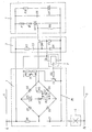
- a control circuit 1 is acted upon by a control signal by an electronic control switch 2 in accordance with its switch position and, depending on this, passes on a control signal of its own to a power switching part 4.
- the power switching part 4 connects a load 6, which lies on the neutral conductor N of a network 5, to the phase conductor L of this network.
- a power supply circuit 3 generates the supply voltage required by the control switch 2 and by the control circuit 1.
- the connection between the power switching part 4 and the load 6 forms a common reference potential M for all modules 1, 2, 3, 4, 6.
- An ignition capacitor C1 is also connected to the reference potential M and is connected to the phase conductor L via a series resistor R1.
- a rectifier bridge circuit formed from four diodes D1, D2, D3, D4 lies with its one AC voltage input, which is formed by the diodes D1, D2, between the ignition capacitor C1 and the series resistor R1.
- the other AC voltage input formed by the diodes D3, D4 is connected to the control input of the power switching part 4.
- a trigger diode D5 is connected to the positive output of the bridge rectifier formed by the two diodes D1, D3. With this connected in series is the switching path of a thyristor V1, which is connected with its cathode to the negative output of the bridge rectifier formed by the two diodes D2, D4.
- the trigger diode D5 can also be arranged between the ignition capacitor C1 and the AC voltage connection formed by D1 and D2.
- control circuit 1 also includes a driver circuit consisting of two complementary transistor stages.
- the collector of a pnp transistor T1 is connected via a resistor R3 to the gate of the thyristor Vl, while its emitter is connected to the output of the power supply circuit 3, which outputs an output voltage U V.
- An npn transistor T2 is connected via its emitter to reference potential M, while its collector is connected to the base of the pnp transistor T2 via a resistor R5.
- the base is in turn connected to the output U V of the power supply circuit 3 via a resistor R4, and the output of the control switch 2 is supplied to the base of the npn transistor T2 via a resistor R6.
- the control switch 2 is an electronic switch, the z. B. is equipped as a motion detector with an infrared detector and emits a control signal to the control circuit 1 upon detection of the thermal radiation emanating from a radiation object. Like this, it is supplied with the voltage U V by the power supply circuit 3.
- the power supply circuit 3 is connected via a resistor R7 to the phase conductor L of the network and to the anode of a zener diode D6 with the reference potential M. Between these two components there is a charging capacitor C3 in series, and parallel to the zener diode D6 is the series connection of a diode D7 and a capacitor C4, which is connected to reference potential M. Zener diode D6 and diode D7 are polarized so that the buffer capacitor C4 charges during the positive half-wave of the AC voltage to a positive voltage U V , which corresponds approximately to the Zener voltage.
- the control input of the power switching part 4 is identical to the gate of a thyristor V2, which is connected to the reference potential M via a resistor R8.
- the section of the power thyristor V2, which is also connected on one side to zero potential, is in series with the phase conductor L with a suppression choke E and a fuse F.
- an interference suppression capacitor C5 Parallel to this series connection, i.e. also between phase conductor L and reference potential M, an interference suppression capacitor C5 is used, to which in turn one Series connection of a resistor R9 and a suppressor diode D8 is connected in parallel.
- the voltage value 0 is present at its Q output.
- the transistors T2 and T1 are thus blocked in the control circuit 1.
- the thyristor V1 receives no gate current. No ignition current can therefore flow from the network via the bridge branch D5, V1 into the gate of the power triac V2, which means that it remains blocked.
- R2 forms the terminating resistor necessary at the gate of thyristor V1.
- the capacitor C2 short-circuits voltage peaks coupled in from the network and prevents unwanted ignitions.
- the necessary gate current (e.g. approx. 200 ⁇ A) flows into the thyristor V1, making it conductive.
- the gate current is taken from the supply circuit 3. He finds his way out of the bridge over D4 and R8 to the reference potential M.
- the ignition current required for the triac V2 only flows through the thyristor V1 when the mains voltage has reached the breakdown voltage of the trigger diode D5 (here, for example, 36 V) and the diode paths.
- the ignition current is then emitted from the capacitor C1, which has been charged up to the breakdown voltage of the trigger diode D5, via D1, D5, V1, D4 to the gate of the power triac V2 (approx. 100 mA). This will ignite it safely and remain conductive during the positive half-wave.
- the power triac V2 switches off at the beginning of the negative mains half-wave, i.e. at zero crossing.
- the following curve is shown:
- the supply voltage U V tries to let a current flow into the gate of the thyristor V1 via T1, R3. This actually succeeds because this current can then leave the bridge via D2 and R1 to the phase conductor L, which now has a negative potential. That is, a gate current is set at thyristor V1, which increases continuously as long as the breakdown voltage of trigger diode D5 has not yet been reached. Before this point is reached, a resulting gate current (approx. 1 mA) results according to the following approximation equation
- the power triac V2 When the trigger voltage is reached, i.e. the breakdown voltage of the trigger diode D5, the power triac V2 receives its ignition pulse from C1 via D3, D5, V1 and D2. The power triac V2 remains conductive during the negative half-wave.
- the gate current (from V1) always flows at the same level (e.g. 200 ⁇ A) via R3, V1 and R8 during the positive and negative half-wave , whereby an asymmetry is largely avoided.
- This current then causes a voltage drop (approx. 50 mV) across the resistor R8, which makes it impossible to ignite the power triac V2 prematurely.
- Resistor R1 could also have the value zero (100% symmetry). However, a certain resistance value (here, for example, 10 k ⁇ ) is useful in order to prevent undesired switching of the bridge branch D5, V1 as a result of high-voltage peaks.
- the combination R1 - C1 is connected to the mains voltage.
- the capacitor C1 is alternately charged positively and negatively via the resistor R1 until the trigger voltage at the trigger diode D5 is reached.
- the trigger diode D5 is inserted immediately before the first AC voltage input of the rectifier bridge D1-D4.
- the gate current of the thyristor V1 flows during the positive and negative half-wave at the same level of z. B. 200 ⁇ A via R3, V1, D4 and R8.
- This current causes a voltage drop of approx. 50mV at R8; an early ignition of the power triac V2 is not possible.
Landscapes
- Power Conversion In General (AREA)
- Control Of Ac Motors In General (AREA)
- Semiconductor Integrated Circuits (AREA)
Priority Applications (1)
| Application Number | Priority Date | Filing Date | Title |
|---|---|---|---|
| AT88120573T ATE102773T1 (de) | 1987-12-22 | 1988-12-09 | Schaltungsanordnung zur steuerung eines leistungstriacs. |
Applications Claiming Priority (2)
| Application Number | Priority Date | Filing Date | Title |
|---|---|---|---|
| DE3743556 | 1987-12-22 | ||
| DE19873743556 DE3743556A1 (de) | 1987-12-22 | 1987-12-22 | Schaltungsanordnung zur steuerung eines leistungstriacs |
Publications (3)
| Publication Number | Publication Date |
|---|---|
| EP0321798A2 true EP0321798A2 (fr) | 1989-06-28 |
| EP0321798A3 EP0321798A3 (en) | 1990-12-27 |
| EP0321798B1 EP0321798B1 (fr) | 1994-03-09 |
Family
ID=6343284
Family Applications (1)
| Application Number | Title | Priority Date | Filing Date |
|---|---|---|---|
| EP88120573A Expired - Lifetime EP0321798B1 (fr) | 1987-12-22 | 1988-12-09 | Montage pour la commande d'un triac de puissance |
Country Status (6)
| Country | Link |
|---|---|
| EP (1) | EP0321798B1 (fr) |
| AT (1) | ATE102773T1 (fr) |
| DE (2) | DE3743556A1 (fr) |
| DK (1) | DK714188A (fr) |
| ES (1) | ES2052680T3 (fr) |
| NO (1) | NO172668C (fr) |
Cited By (3)
| Publication number | Priority date | Publication date | Assignee | Title |
|---|---|---|---|---|
| WO1995031040A1 (fr) * | 1994-05-06 | 1995-11-16 | Fazakas Andras | Commutateur a caracteristiques de montee et de descente commandees |
| WO1999003027A1 (fr) * | 1997-07-09 | 1999-01-21 | H.P.M. Industries Pty. Ltd. | Interrupteur a semi-conducteurs |
| AU733423B2 (en) * | 1997-07-09 | 2001-05-17 | H.P.M. Industries Pty Limited | Solid state switching device circuit |
Families Citing this family (3)
| Publication number | Priority date | Publication date | Assignee | Title |
|---|---|---|---|---|
| DE4117122A1 (de) * | 1991-05-25 | 1992-11-26 | Abb Patent Gmbh | Schaltung zur steuerung eines wechselstromes |
| DE10148644B4 (de) * | 2001-10-02 | 2017-07-27 | Seuffer gmbH & Co. KG | Elektrische Schaltung zum Dimmen der beiden Halbwellen einer Wechselspannung |
| CN113067570B (zh) * | 2021-03-31 | 2023-07-07 | 樊娜 | 一种应用于交流供电系统的电子墙壁开关 |
Family Cites Families (11)
| Publication number | Priority date | Publication date | Assignee | Title |
|---|---|---|---|---|
| US4008416A (en) * | 1973-05-29 | 1977-02-15 | Nakasone Henry H | Circuit for producing a gradual change in conduction angle |
| FR2271712A1 (en) * | 1974-05-15 | 1975-12-12 | Silec Semi Conducteurs | Static electronic device for timing control - is insensitive to parasitic signals and independent of characteristics of static switch |
| GB1527097A (en) * | 1974-11-29 | 1978-10-04 | Omron Tateisi Electronics Co | Solid state switching circuits |
| US3940634A (en) * | 1975-02-14 | 1976-02-24 | Rockwell International Corporation | Solid state AC power relay |
| US4158150A (en) * | 1978-01-10 | 1979-06-12 | Amf Incorporated | Solid state relay with zero crossover feature |
| US4239986A (en) * | 1978-09-08 | 1980-12-16 | Hyrbrinetics, Inc. | Power control arrangement and control circuit especially suitable for use therewith |
| FR2448805A1 (fr) * | 1979-02-08 | 1980-09-05 | Silicium Semiconducteur Ssc | Circuit anti-parasites pour gradateur de lumiere |
| DE2942662A1 (de) * | 1979-06-28 | 1981-05-07 | Eberhard Dipl.-Phys. 7257 Ditzingen Pechhold | Dimmerschaltung mit zeitverhalten |
| JPS5680929A (en) * | 1979-12-04 | 1981-07-02 | Nippon Gakki Seizo Kk | Triggering circuit for two-way thyristor such as triac |
| JPS59215696A (ja) * | 1983-05-21 | 1984-12-05 | 林原 健 | 高輝度電球用電源装置 |
| DE3615052A1 (de) * | 1986-05-03 | 1987-11-05 | Balluff Gebhard Feinmech | Zweidraht-schalter |
-
1987
- 1987-12-22 DE DE19873743556 patent/DE3743556A1/de not_active Withdrawn
-
1988
- 1988-12-09 EP EP88120573A patent/EP0321798B1/fr not_active Expired - Lifetime
- 1988-12-09 ES ES88120573T patent/ES2052680T3/es not_active Expired - Lifetime
- 1988-12-09 DE DE88120573T patent/DE3888326D1/de not_active Expired - Fee Related
- 1988-12-09 AT AT88120573T patent/ATE102773T1/de active
- 1988-12-20 NO NO885644A patent/NO172668C/no unknown
- 1988-12-21 DK DK714188A patent/DK714188A/da not_active Application Discontinuation
Cited By (5)
| Publication number | Priority date | Publication date | Assignee | Title |
|---|---|---|---|---|
| WO1995031040A1 (fr) * | 1994-05-06 | 1995-11-16 | Fazakas Andras | Commutateur a caracteristiques de montee et de descente commandees |
| WO1999003027A1 (fr) * | 1997-07-09 | 1999-01-21 | H.P.M. Industries Pty. Ltd. | Interrupteur a semi-conducteurs |
| GB2341990A (en) * | 1997-07-09 | 2000-03-29 | Hpm Ind Pty Ltd | Solid state switching device circuit |
| AU733423B2 (en) * | 1997-07-09 | 2001-05-17 | H.P.M. Industries Pty Limited | Solid state switching device circuit |
| GB2341990B (en) * | 1997-07-09 | 2001-06-13 | Hpm Ind Pty Ltd | Solid state switching device circuit |
Also Published As
| Publication number | Publication date |
|---|---|
| NO172668C (no) | 1993-08-18 |
| EP0321798B1 (fr) | 1994-03-09 |
| NO172668B (no) | 1993-05-10 |
| NO885644D0 (no) | 1988-12-20 |
| ES2052680T3 (es) | 1994-07-16 |
| DE3888326D1 (de) | 1994-04-14 |
| DK714188A (da) | 1989-06-23 |
| EP0321798A3 (en) | 1990-12-27 |
| ATE102773T1 (de) | 1994-03-15 |
| DK714188D0 (da) | 1988-12-21 |
| DE3743556A1 (de) | 1989-07-13 |
| NO885644L (no) | 1989-06-23 |
Similar Documents
| Publication | Publication Date | Title |
|---|---|---|
| EP0176800B1 (fr) | Procédé et dispositif pour contrôler l'état d'un thyristor blocable | |
| EP0244743B1 (fr) | Commutateur à deux fils | |
| DE2738186A1 (de) | Nullschaltspannungs-festkoerper-relais | |
| DE3840406C2 (fr) | ||
| DE2263867A1 (de) | Steuerschaltung fuer thyristoren | |
| DE2753869C2 (de) | Meßwertgeber | |
| DE2939250C2 (de) | Annäherungsschalter | |
| EP0321798B1 (fr) | Montage pour la commande d'un triac de puissance | |
| DE3045798A1 (de) | Zweirichtungsschalter | |
| DE2506196C2 (de) | Gleichstrom-Schaltvorrichtung zur Erhöhung des Spitzenstromes | |
| EP0219074A2 (fr) | Commutateur du type à deux fils avec un transistor de puissance | |
| DE3917062A1 (de) | Lichtblitzwarnanlage | |
| EP0339598A2 (fr) | Circuit de protection pour charges inductives | |
| DE2814904A1 (de) | Elektrischer schalter | |
| DE69023877T2 (de) | Selbstversorgte SCR-Gateansteuerschaltung mit optischer Isolation. | |
| DE1903621A1 (de) | Thyristor-Ansteuerschaltung | |
| DE3115214A1 (de) | Schaltungsanordnung zum schutze eines elektronischen zweidraht-wechselstromschalters gegen ueberlastung | |
| EP0489935B1 (fr) | Commutateur MOSFET pour une charge inductive | |
| EP0622902A2 (fr) | Relais semi-conducteur | |
| DE2813073A1 (de) | Diskriminator-schaltung | |
| DE2832193A1 (de) | Kontaktloses relais | |
| DE2360392C2 (de) | Einrichtung zur Steuerung eines Thyristors | |
| DE2553389B2 (de) | Halbleiterschaltschaltung | |
| EP2140735B1 (fr) | Ensemble circuit servant à amorcer et à faire fonctionner au moins une lampe à décharge | |
| DE69007138T2 (de) | Motorregler mit siliciumgesteuerten Gleichrichtern. |
Legal Events
| Date | Code | Title | Description |
|---|---|---|---|
| PUAI | Public reference made under article 153(3) epc to a published international application that has entered the european phase |
Free format text: ORIGINAL CODE: 0009012 |
|
| AK | Designated contracting states |
Kind code of ref document: A2 Designated state(s): AT BE CH DE ES FR GB IT LI NL SE |
|
| PUAL | Search report despatched |
Free format text: ORIGINAL CODE: 0009013 |
|
| AK | Designated contracting states |
Kind code of ref document: A3 Designated state(s): AT BE CH DE ES FR GB IT LI NL SE |
|
| 16A | New documents despatched to applicant after publication of the search report | ||
| 17P | Request for examination filed |
Effective date: 19910605 |
|
| 17Q | First examination report despatched |
Effective date: 19930405 |
|
| GRAA | (expected) grant |
Free format text: ORIGINAL CODE: 0009210 |
|
| AK | Designated contracting states |
Kind code of ref document: B1 Designated state(s): AT BE CH DE ES FR GB IT LI NL SE |
|
| REF | Corresponds to: |
Ref document number: 102773 Country of ref document: AT Date of ref document: 19940315 Kind code of ref document: T |
|
| REF | Corresponds to: |
Ref document number: 3888326 Country of ref document: DE Date of ref document: 19940414 |
|
| GBT | Gb: translation of ep patent filed (gb section 77(6)(a)/1977) |
Effective date: 19940323 |
|
| ET | Fr: translation filed | ||
| ITF | It: translation for a ep patent filed | ||
| REG | Reference to a national code |
Ref country code: ES Ref legal event code: FG2A Ref document number: 2052680 Country of ref document: ES Kind code of ref document: T3 |
|
| PLBE | No opposition filed within time limit |
Free format text: ORIGINAL CODE: 0009261 |
|
| STAA | Information on the status of an ep patent application or granted ep patent |
Free format text: STATUS: NO OPPOSITION FILED WITHIN TIME LIMIT |
|
| EAL | Se: european patent in force in sweden |
Ref document number: 88120573.6 |
|
| 26N | No opposition filed | ||
| PGFP | Annual fee paid to national office [announced via postgrant information from national office to epo] |
Ref country code: GB Payment date: 19961014 Year of fee payment: 9 |
|
| PGFP | Annual fee paid to national office [announced via postgrant information from national office to epo] |
Ref country code: NL Payment date: 19961021 Year of fee payment: 9 |
|
| PGFP | Annual fee paid to national office [announced via postgrant information from national office to epo] |
Ref country code: SE Payment date: 19961024 Year of fee payment: 9 Ref country code: FR Payment date: 19961024 Year of fee payment: 9 Ref country code: AT Payment date: 19961024 Year of fee payment: 9 |
|
| PGFP | Annual fee paid to national office [announced via postgrant information from national office to epo] |
Ref country code: CH Payment date: 19961029 Year of fee payment: 9 |
|
| PGFP | Annual fee paid to national office [announced via postgrant information from national office to epo] |
Ref country code: ES Payment date: 19961224 Year of fee payment: 9 |
|
| PG25 | Lapsed in a contracting state [announced via postgrant information from national office to epo] |
Ref country code: GB Free format text: LAPSE BECAUSE OF NON-PAYMENT OF DUE FEES Effective date: 19971209 Ref country code: AT Free format text: LAPSE BECAUSE OF NON-PAYMENT OF DUE FEES Effective date: 19971209 |
|
| PG25 | Lapsed in a contracting state [announced via postgrant information from national office to epo] |
Ref country code: SE Free format text: LAPSE BECAUSE OF NON-PAYMENT OF DUE FEES Effective date: 19971210 Ref country code: ES Free format text: LAPSE BECAUSE OF EXPIRATION OF PROTECTION Effective date: 19971210 |
|
| PG25 | Lapsed in a contracting state [announced via postgrant information from national office to epo] |
Ref country code: LI Free format text: LAPSE BECAUSE OF NON-PAYMENT OF DUE FEES Effective date: 19971231 Ref country code: FR Free format text: THE PATENT HAS BEEN ANNULLED BY A DECISION OF A NATIONAL AUTHORITY Effective date: 19971231 Ref country code: CH Free format text: LAPSE BECAUSE OF NON-PAYMENT OF DUE FEES Effective date: 19971231 |
|
| PG25 | Lapsed in a contracting state [announced via postgrant information from national office to epo] |
Ref country code: NL Free format text: LAPSE BECAUSE OF NON-PAYMENT OF DUE FEES Effective date: 19980701 |
|
| GBPC | Gb: european patent ceased through non-payment of renewal fee |
Effective date: 19971209 |
|
| REG | Reference to a national code |
Ref country code: CH Ref legal event code: PL |
|
| NLV4 | Nl: lapsed or anulled due to non-payment of the annual fee |
Effective date: 19980701 |
|
| EUG | Se: european patent has lapsed |
Ref document number: 88120573.6 |
|
| REG | Reference to a national code |
Ref country code: FR Ref legal event code: ST |
|
| PGFP | Annual fee paid to national office [announced via postgrant information from national office to epo] |
Ref country code: BE Payment date: 19981109 Year of fee payment: 11 |
|
| PG25 | Lapsed in a contracting state [announced via postgrant information from national office to epo] |
Ref country code: BE Free format text: LAPSE BECAUSE OF NON-PAYMENT OF DUE FEES Effective date: 19991231 |
|
| BERE | Be: lapsed |
Owner name: ASEA BROWN BOVERI A.G. Effective date: 19991231 |
|
| REG | Reference to a national code |
Ref country code: ES Ref legal event code: FD2A Effective date: 20010201 |
|
| PGFP | Annual fee paid to national office [announced via postgrant information from national office to epo] |
Ref country code: DE Payment date: 20041213 Year of fee payment: 17 |
|
| PG25 | Lapsed in a contracting state [announced via postgrant information from national office to epo] |
Ref country code: IT Free format text: LAPSE BECAUSE OF NON-PAYMENT OF DUE FEES;WARNING: LAPSES OF ITALIAN PATENTS WITH EFFECTIVE DATE BEFORE 2007 MAY HAVE OCCURRED AT ANY TIME BEFORE 2007. THE CORRECT EFFECTIVE DATE MAY BE DIFFERENT FROM THE ONE RECORDED. Effective date: 20051209 |
|
| PG25 | Lapsed in a contracting state [announced via postgrant information from national office to epo] |
Ref country code: DE Free format text: LAPSE BECAUSE OF NON-PAYMENT OF DUE FEES Effective date: 20060701 |