EP0489935B1 - Commutateur MOSFET pour une charge inductive - Google Patents
Commutateur MOSFET pour une charge inductive Download PDFInfo
- Publication number
- EP0489935B1 EP0489935B1 EP90121498A EP90121498A EP0489935B1 EP 0489935 B1 EP0489935 B1 EP 0489935B1 EP 90121498 A EP90121498 A EP 90121498A EP 90121498 A EP90121498 A EP 90121498A EP 0489935 B1 EP0489935 B1 EP 0489935B1
- Authority
- EP
- European Patent Office
- Prior art keywords
- voltage
- inductive load
- current
- source
- zener diode
- Prior art date
- Legal status (The legal status is an assumption and is not a legal conclusion. Google has not performed a legal analysis and makes no representation as to the accuracy of the status listed.)
- Expired - Lifetime
Links
Images
Classifications
-
- H—ELECTRICITY
- H03—ELECTRONIC CIRCUITRY
- H03K—PULSE TECHNIQUE
- H03K17/00—Electronic switching or gating, i.e. not by contact-making and –breaking
- H03K17/08—Modifications for protecting switching circuit against overcurrent or overvoltage
- H03K17/082—Modifications for protecting switching circuit against overcurrent or overvoltage by feedback from the output to the control circuit
- H03K17/0822—Modifications for protecting switching circuit against overcurrent or overvoltage by feedback from the output to the control circuit in field-effect transistor switches
-
- H—ELECTRICITY
- H03—ELECTRONIC CIRCUITRY
- H03K—PULSE TECHNIQUE
- H03K17/00—Electronic switching or gating, i.e. not by contact-making and –breaking
- H03K17/06—Modifications for ensuring a fully conducting state
- H03K17/063—Modifications for ensuring a fully conducting state in field-effect transistor switches
-
- H—ELECTRICITY
- H03—ELECTRONIC CIRCUITRY
- H03K—PULSE TECHNIQUE
- H03K17/00—Electronic switching or gating, i.e. not by contact-making and –breaking
- H03K17/51—Electronic switching or gating, i.e. not by contact-making and –breaking characterised by the components used
- H03K17/56—Electronic switching or gating, i.e. not by contact-making and –breaking characterised by the components used by the use, as active elements, of semiconductor devices
- H03K17/687—Electronic switching or gating, i.e. not by contact-making and –breaking characterised by the components used by the use, as active elements, of semiconductor devices the devices being field-effect transistors
- H03K17/6877—Electronic switching or gating, i.e. not by contact-making and –breaking characterised by the components used by the use, as active elements, of semiconductor devices the devices being field-effect transistors the control circuit comprising active elements different from those used in the output circuit
Definitions
- the invention relates to a circuit arrangement with a power MOSFET and an inductive load, which is connected on the one hand to the source connection and on the other hand to a terminal which is at a fixed potential, and with a Zener diode and a controllable switch for switching off the inductive load.
- Switch existing series circuit which is connected between the gate connection and the terminal.
- the gate connection of the power MOSFET is at zero volts in the switched-off state. If the voltage at the inductive load reverses, the power MOSFET can switch on again before the zener diode reaches its zener voltage if its source potential has dropped below zero by the threshold voltage.
- the driving voltage at the inductive load is therefore limited in this case to a value that corresponds to the threshold voltage of the power MOSFET. The magnetic energy is therefore only slowly reduced in this case.
- the aim of the invention is to develop a circuit arrangement of the type described so that switching on of the power MOSFET is reliably prevented as long as the voltage applied to the zener diode in the blocking direction is below the zener voltage.
- This goal is achieved by a controllable resistance between the gate connection and the source connection, the resistance value of which, when the load is switched off, is controlled in such a way that it has a first high value when a current flows when the Zener diode breaks down and a second, lower value below this current.
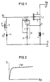
- FIGS. 1 and 2 show a circuit arrangement according to the invention and FIG. 2 shows the U / I characteristic of a controllable resistor.
- the circuit arrangement according to FIG. 1 contains a power MOSFET 1 to which an inductive load 2 is connected in series on the source side.
- the series connection is connected to an operating voltage V DD via two terminals 12, 13.
- the terminal 13 is at a fixed potential, for. B. to ground.
- a series circuit consisting of a MOSFET 3 and a Zener diode 4 is connected between the gate connection of the power MOSFET 1 and the terminal 13.
- the zener diode 4 is polarized such that it is stressed in the reverse direction by the driving voltage generated when the inductive load 2 is switched off.
- the gate connection of the power MOSFET is connected to a terminal 10, the gate connection of the MOSFET 3 to a terminal 11.
- An n-channel depletion MOSFET 5 is located between the gate connection and the source connection of the power MOSFET 1.
- the source connection of the depletion MOSFET 5 is connected to its substrate. Its gate connection is connected to the tap of a voltage divider 6, which is connected in parallel with the inductive load 2.
- the voltage divider 6 consists of a Zener diode 7 and a resistor 8. However, the Zener diode 7 can also be replaced by a resistor.
- a positive voltage is applied to the terminal 10, which is greater than the operating voltage V DD .
- You can e.g. B. can be supplied by a known pump circuit.
- the controllable switch 3 is controlled to be conductive by a voltage applied to the terminal 11.
- the gate-source capacitance of the power MOSFET 1 is thus discharged and the latter begins to block.
- a voltage with the drawn polarity builds up on the inductive load 2.
- the voltage at the source terminal of the power MOSFET 1 (node 9) thus becomes negative with respect to its gate voltage, since its gate is at zero volts via the terminal 10.
- the power MOSFET 1 could thus be switched on again.
- This is switched as a current source; its source is connected to the substrate. It is dimensioned such that its saturation current I sat (FIG 2) is greater than the reverse current which flows through the Zener diode 4 if it has not yet broken down. However, the saturation current is less than the current that would flow if the Zener diode 4 breaks down.
- the voltage present at the inductive load 2 after switching on the MOSFET 3 and blocking the power MOSFET 1 first drives a current through the Zener diode 4, the MOSFET 3 and the depletion FET 5, which is less than the saturation current of the depletion FET. Therefore, only a low drain-source voltage drops across it. The gate connection and the source connection of the power MOSFET 1 are thus practically at the same potential, so that it remains blocked. If the voltage across the inductive load 2 continues to rise, the Zener voltage U Z of the Zener diode 4 is reached and this breaks down. So that increases current driven by the zener diode 4, the MOSFET 3 and the depletion FET 5 until the saturation current of the depletion FET is reached.
- the drain-source voltage of the depletion FET increases and the power MOSFET 1 is turned on when its threshold voltage is reached.
- the current of the inductive load 2 can thus flow through the operating voltage source and the power MOSFET 1.
- the driving voltage is determined by the voltage U Z plus the drain-source voltage of the controllable switch 3 plus the drain-source voltage of the depletion FET 5. It can be set by selecting the Zener diode 4 accordingly.
- the depletion FET In order to reliably block the depletion FET when the load 2 is switched on, it must have a high forward resistance when the control voltage is applied to the terminal 10. This is achieved in that its gate connection is negatively biased with respect to its source connection via the voltage divider 6. The depletion FET 5 is thus blocked as long as the voltage at node 9 is more positive than at terminal 13.
- the MOSFET 3 can by another controllable switch, for. B. be replaced by a bipolar transistor.
- the depletion FET 5 can also be controlled by another controllable resistor. B. a bipolar transistor can be replaced.
Claims (4)
- Montage comportant un transistor MOSFET de puissance (1) et une charge inductive (2), qui est reliée, d'une part, à la borne de source et, d'autre part, à une borne (13) placée à un potentiel fixe, et un circuit série formé d'une diode Zener (4) et d'un interrupteur commandable (3) servant à débrancher la charge inductive (2) et qui est branché entre la borne de grille et la borne (13),
caractérisé par une résistance commandable (5) disposée entre la borne de grille et la borne de source et dont la valeur résistive est commandée, lors du débranchement de la charge (2), de manière à posséder une première valeur élevée pour un courant circulant lors du claquage de la diode Zener (4), et, au-dessous de ce courant une seconde valeur plus faible. - Montage suivant la revendication 1, caractérisé par le fait que la résistance commandable est une source de courant, dont le courant est inférieur au courant circulant lors du claquage de la diode Zener.
- Montage suivant la revendication 2, caractérisé par le fait que la source de courant est un transistor FET à appauvrissement (5), dont le courant de saturation est inférieur au courant circulant lors du claquage de la diode Zener.
- Montage suivant la revendication 3, caractérisé par le fait que la borne de grille du transistor FET à appauvrissement (5) est reliée à la prise d'un diviseur de tension (6), qui est branché en parallèle avec la charge inductive (2).
Priority Applications (4)
| Application Number | Priority Date | Filing Date | Title |
|---|---|---|---|
| DE59009841T DE59009841D1 (de) | 1990-11-09 | 1990-11-09 | MOSFET-Schalter für eine induktive Last. |
| EP90121498A EP0489935B1 (fr) | 1990-11-09 | 1990-11-09 | Commutateur MOSFET pour une charge inductive |
| JP31362091A JP3258050B2 (ja) | 1990-11-09 | 1991-10-31 | 誘導性負荷用mosfetを備えた回路装置 |
| US07/788,594 US5160862A (en) | 1990-11-09 | 1991-11-06 | Mosfet switch circuit for preventing the switch being turned on during deactivation of an inductive load |
Applications Claiming Priority (1)
| Application Number | Priority Date | Filing Date | Title |
|---|---|---|---|
| EP90121498A EP0489935B1 (fr) | 1990-11-09 | 1990-11-09 | Commutateur MOSFET pour une charge inductive |
Publications (2)
| Publication Number | Publication Date |
|---|---|
| EP0489935A1 EP0489935A1 (fr) | 1992-06-17 |
| EP0489935B1 true EP0489935B1 (fr) | 1995-11-02 |
Family
ID=8204701
Family Applications (1)
| Application Number | Title | Priority Date | Filing Date |
|---|---|---|---|
| EP90121498A Expired - Lifetime EP0489935B1 (fr) | 1990-11-09 | 1990-11-09 | Commutateur MOSFET pour une charge inductive |
Country Status (4)
| Country | Link |
|---|---|
| US (1) | US5160862A (fr) |
| EP (1) | EP0489935B1 (fr) |
| JP (1) | JP3258050B2 (fr) |
| DE (1) | DE59009841D1 (fr) |
Families Citing this family (6)
| Publication number | Priority date | Publication date | Assignee | Title |
|---|---|---|---|---|
| US5430401A (en) * | 1992-08-27 | 1995-07-04 | Northern Telecom Ltd. | Electronic switches |
| JPH06252727A (ja) * | 1993-02-10 | 1994-09-09 | Siemens Ag | Mos半導体素子の制御回路 |
| DE4329981A1 (de) * | 1993-09-04 | 1995-03-09 | Bosch Gmbh Robert | Verfahren und Vorrichtung zur Ansteuerung eines elektromagnetischen Verbrauchers |
| DE19838109B4 (de) * | 1998-08-21 | 2005-10-27 | Infineon Technologies Ag | Ansteuerschaltung für induktive Lasten |
| US7834669B2 (en) * | 2007-12-21 | 2010-11-16 | Nec Electronics Corporation | Semiconductor output circuit for controlling power supply to a load |
| JP6515241B1 (ja) | 2018-03-02 | 2019-05-15 | 田中精密工業株式会社 | 接着剤塗布装置及び接着剤塗布方法 |
Family Cites Families (7)
| Publication number | Priority date | Publication date | Assignee | Title |
|---|---|---|---|---|
| JPS5855582B2 (ja) * | 1981-11-13 | 1983-12-10 | 株式会社東芝 | 透視性テ−プカセツト |
| US4691129A (en) * | 1986-03-19 | 1987-09-01 | Siemens Aktiengesellschaft | Drive circuit for a power MOSFET with source-side load |
| US4728826A (en) * | 1986-03-19 | 1988-03-01 | Siemens Aktiengesellschaft | MOSFET switch with inductive load |
| US4808839A (en) * | 1988-04-04 | 1989-02-28 | Motorola, Inc. | Power field effect transistor driver circuit for protection from overvoltages |
| IT1226557B (it) * | 1988-07-29 | 1991-01-24 | Sgs Thomson Microelectronics | Circuito di controllo della tensione di bloccaggio di un carico induttivo pilotato con un dispositivo di potenza in configurazione "high side driver" |
| EP0369048A1 (fr) * | 1988-11-15 | 1990-05-23 | Siemens Aktiengesellschaft | Montage de régulation du courant de charge dans un MOSFET de puissance |
| US5017816A (en) * | 1989-11-08 | 1991-05-21 | National Semiconductor Corp. | Adaptive gate discharge circuit for power FETS |
-
1990
- 1990-11-09 DE DE59009841T patent/DE59009841D1/de not_active Expired - Lifetime
- 1990-11-09 EP EP90121498A patent/EP0489935B1/fr not_active Expired - Lifetime
-
1991
- 1991-10-31 JP JP31362091A patent/JP3258050B2/ja not_active Expired - Lifetime
- 1991-11-06 US US07/788,594 patent/US5160862A/en not_active Expired - Fee Related
Also Published As
| Publication number | Publication date |
|---|---|
| EP0489935A1 (fr) | 1992-06-17 |
| JP3258050B2 (ja) | 2002-02-18 |
| JPH04268813A (ja) | 1992-09-24 |
| DE59009841D1 (de) | 1995-12-07 |
| US5160862A (en) | 1992-11-03 |
Similar Documents
| Publication | Publication Date | Title |
|---|---|---|
| EP0572706B1 (fr) | Circuit de commande pour un transistor à effet de champ de puissance dont le source et connectée à une charge | |
| EP0043489B1 (fr) | Commutateur avec des transistors à effet de champ MOS connectés en série | |
| EP1074081B1 (fr) | Circuit a protection contre l'inversion de polarite | |
| DE4432957C1 (de) | Schaltmittel | |
| EP0244743B1 (fr) | Commutateur à deux fils | |
| EP0108283A2 (fr) | Commutateur électronique | |
| EP0236967B1 (fr) | Montage pour la commande d'un MOSFET dont la source est connectée à une charge | |
| DE102014108576A1 (de) | Treiberschaltung mit Miller-Clamping-Funktionalität für Leistungshalbleiterschalter, Leistungshalbleiterschalter und Wechselrichterbrücke | |
| DE19631751C1 (de) | Ansteuerschaltung für einen Leistungs-FET mit sourceseitiger Last | |
| EP0489935B1 (fr) | Commutateur MOSFET pour une charge inductive | |
| DE3100795C2 (fr) | ||
| EP0405407A2 (fr) | Montage pour la commande d'un MOSFET à charge connectée à la source | |
| DE4429285C1 (de) | Ansteuerschaltung für ein feldeffektgesteuertes Leistungs-Halbleiterbauelement | |
| EP0354478A1 (fr) | Circuit de protection pour un MOSFET de puissance entre grille et source | |
| DE3128013C1 (de) | Ansteuerschaltung fuer wenigstens eine lichtemittierende Diode | |
| DE4035969A1 (de) | Schaltungsanordnung mit wenigstens einer einen leistungs-mosfet enthaltenden schaltvorrichtung | |
| DE2135858C3 (de) | Transistorschalteinrichtung zum Schalten eines induktiven Gleichstromkreises | |
| EP0365706A1 (fr) | Etage de sortie de puissance avec une charge | |
| EP0082422A1 (fr) | Circuit pour un transistor de puissance de type FET | |
| DE3536447C2 (de) | Kurzschluß- und überlastfeste Transistorausgangsstufe | |
| EP0822661A2 (fr) | Circuit d'attaque pour un dispositif semi-conducteur de puissance commandé par effet de champ | |
| EP0766394A2 (fr) | Montage servant à commander un transistor à effet de champ MOS de puissance à enrichissement | |
| DE102004022800A1 (de) | MOSFET-Gate-Treiberschaltung | |
| EP0555648A2 (fr) | Circuit pour commander des commutateurs de puissance commandés par effet de champ | |
| DE19535985B4 (de) | Schaltungsanordnung zum Ansteuern eines FET |
Legal Events
| Date | Code | Title | Description |
|---|---|---|---|
| PUAI | Public reference made under article 153(3) epc to a published international application that has entered the european phase |
Free format text: ORIGINAL CODE: 0009012 |
|
| 17P | Request for examination filed |
Effective date: 19901205 |
|
| AK | Designated contracting states |
Kind code of ref document: A1 Designated state(s): AT BE CH DE DK ES FR GB GR IT LI LU NL SE |
|
| RBV | Designated contracting states (corrected) |
Designated state(s): DE FR IT |
|
| 17Q | First examination report despatched |
Effective date: 19950405 |
|
| GRAA | (expected) grant |
Free format text: ORIGINAL CODE: 0009210 |
|
| AK | Designated contracting states |
Kind code of ref document: B1 Designated state(s): DE FR IT |
|
| REF | Corresponds to: |
Ref document number: 59009841 Country of ref document: DE Date of ref document: 19951207 |
|
| ITF | It: translation for a ep patent filed |
Owner name: STUDIO JAUMANN |
|
| ET | Fr: translation filed | ||
| PLBE | No opposition filed within time limit |
Free format text: ORIGINAL CODE: 0009261 |
|
| STAA | Information on the status of an ep patent application or granted ep patent |
Free format text: STATUS: NO OPPOSITION FILED WITHIN TIME LIMIT |
|
| 26N | No opposition filed | ||
| PGFP | Annual fee paid to national office [announced via postgrant information from national office to epo] |
Ref country code: IT Payment date: 20091126 Year of fee payment: 20 Ref country code: FR Payment date: 20091201 Year of fee payment: 20 |
|
| PGFP | Annual fee paid to national office [announced via postgrant information from national office to epo] |
Ref country code: DE Payment date: 20100119 Year of fee payment: 20 |
|
| PG25 | Lapsed in a contracting state [announced via postgrant information from national office to epo] |
Ref country code: DE Free format text: LAPSE BECAUSE OF EXPIRATION OF PROTECTION Effective date: 20101109 |