EP0321136B1 - Low light level solar cell - Google Patents
Low light level solar cell Download PDFInfo
- Publication number
- EP0321136B1 EP0321136B1 EP88311536A EP88311536A EP0321136B1 EP 0321136 B1 EP0321136 B1 EP 0321136B1 EP 88311536 A EP88311536 A EP 88311536A EP 88311536 A EP88311536 A EP 88311536A EP 0321136 B1 EP0321136 B1 EP 0321136B1
- Authority
- EP
- European Patent Office
- Prior art keywords
- silicon
- photovoltaic
- film
- doped
- layer
- Prior art date
- Legal status (The legal status is an assumption and is not a legal conclusion. Google has not performed a legal analysis and makes no representation as to the accuracy of the status listed.)
- Expired - Lifetime
Links
Images
Classifications
-
- H—ELECTRICITY
- H10—SEMICONDUCTOR DEVICES; ELECTRIC SOLID-STATE DEVICES NOT OTHERWISE PROVIDED FOR
- H10F—INORGANIC SEMICONDUCTOR DEVICES SENSITIVE TO INFRARED RADIATION, LIGHT, ELECTROMAGNETIC RADIATION OF SHORTER WAVELENGTH OR CORPUSCULAR RADIATION
- H10F10/00—Individual photovoltaic cells, e.g. solar cells
- H10F10/10—Individual photovoltaic cells, e.g. solar cells having potential barriers
- H10F10/17—Photovoltaic cells having only PIN junction potential barriers
-
- H—ELECTRICITY
- H10—SEMICONDUCTOR DEVICES; ELECTRIC SOLID-STATE DEVICES NOT OTHERWISE PROVIDED FOR
- H10F—INORGANIC SEMICONDUCTOR DEVICES SENSITIVE TO INFRARED RADIATION, LIGHT, ELECTROMAGNETIC RADIATION OF SHORTER WAVELENGTH OR CORPUSCULAR RADIATION
- H10F77/00—Constructional details of devices covered by this subclass
- H10F77/20—Electrodes
- H10F77/206—Electrodes for devices having potential barriers
- H10F77/211—Electrodes for devices having potential barriers for photovoltaic cells
-
- Y—GENERAL TAGGING OF NEW TECHNOLOGICAL DEVELOPMENTS; GENERAL TAGGING OF CROSS-SECTIONAL TECHNOLOGIES SPANNING OVER SEVERAL SECTIONS OF THE IPC; TECHNICAL SUBJECTS COVERED BY FORMER USPC CROSS-REFERENCE ART COLLECTIONS [XRACs] AND DIGESTS
- Y02—TECHNOLOGIES OR APPLICATIONS FOR MITIGATION OR ADAPTATION AGAINST CLIMATE CHANGE
- Y02E—REDUCTION OF GREENHOUSE GAS [GHG] EMISSIONS, RELATED TO ENERGY GENERATION, TRANSMISSION OR DISTRIBUTION
- Y02E10/00—Energy generation through renewable energy sources
- Y02E10/50—Photovoltaic [PV] energy
- Y02E10/548—Amorphous silicon PV cells
Definitions
- the present invention relates to the field of thin film silicon photovoltaic devices and more particularly to the use of a microcrystalline silicon film as a current collecting film in such devices.
- Pinholes are small spots or holes in the silicon film which leave the front current collecting film exposed. Therefore, when the back-face current collecting film is deposited, it makes a direct contact with the front face film and forms a shunt or short circuit.
- Various techniques have been developed for eliminating or fixing such shunts.
- the typical device structure uses a tin oxide front face contact and an aluminum back-face contact. This structure can be somewhat self fixing because oxygen from the tin oxide tends to form an insulating layer of aluminum oxide at the contact point. This reaction generally forms sufficient insulation to limit the resulting shunt current to an acceptable level in high power devices, that is devices intended for use in direct sun light.
- this type of shunt is unacceptable in devices for low light level, for example indoor, applications such as "solar" powered calculators. For such low light level use, less than 200 lux, essentially no shunting can be tolerated.
- a photovoltaic cell comprising a thin film silicon p-i-n structure having a back face and a front face with back face and front face current collecting electrodes, characterised in that at least one of the p- and n- regions of said p-i-n structure includes or is formed of a doped microcrystalline silicon film having a thickness greater than 50nm, said doped microcrystalline silicon film forming a respective one of said current collecting electrodes.
- a photovoltaic device comprising: a transparent front face electrode; an amorphous silicon thin film photovoltaic layer on said front face electrode; and a back face electrode consisting of a layer of microcrystalline silicon having a thickness greater than 50nm directly contacting said photovoltaic layer.
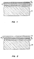
- the photovoltaic device of FIG. 1 is manufactured on a glass substrate 10.
- a device which may be made according to the teachings of the above-referenced Hamakawa patents.
- a first, or front-face, current film 12 of a transparent conductive material such as tin oxide.
- a thin amorphous silicon film 14 having a p-doped region 16, an intrinsic region 18 and an n-doped region 20.
- the device is completed by a second, or back-face, current collecting electrode 22.
- the film 22 is typically formed of a highly conductive metal such as aluminum.
- film 22 is a highly doped microcrystalline silicon film.
- a highly doped microcrystalline silicon film having a thickness of from about 500 to about 5000 angstroms and preferably from about 2000 to 4000 angstroms provides sufficient conductivity for low light level, for example less than 200 lux, applications and that the usual metallic conducting layer can be eliminated.
- FIG. 2 there is illustrated a second embodiment of the present invention. The device of FIG.
- a transparent conductive film 26 is first deposited on the substrate 24.
- a thin silicon film 28 having a somewhat modified p-i-n structure is then deposited on the front-face current collecting layer 26.
- Film 28 includes a p-doped region 30 in contact with the film 26 and an intrinsic region 32. Both regions 30 and 32 are formed of amorphous silicon. If desired, region 30 may include carbon as taught by Hamakawa.
- the silicon film 28 also includes a microcrystalline n-doped region 34. Region 34 is preferably highly doped and is relatively thick having dimensions in the ranges suggested for film 22 of FIG. 1. In the FIG.
- the region 34 forms both the n-type region of the p-i-n silicon diode structure and simultaneously acts as the only back-face current collecting electrode for the photovoltaic device. That is, no metallic or other form of electrical conductor is deposited upon the thin film silicon device 28.
- pinholes are generally caused by the presence of dust particles on a substrate onto which a thin film is being deposited. As the film is deposited, the dust particles mask the substrate and prevent formation of the film at the location of the dust particle. In later processing, the dust particles are removed leaving behind an uncoated or exposed substrate area.
- the silicon film for example film 14 of FIG. 1, is deposited on a substrate coated with a transparent conductor 12. All the layers of silicon film 14, and, in the case of FIG. 1 film 22 can be deposited in a single glow discharge chamber without removal of the substrates.
- any dust particles which are present will therefore form pinholes through all of the silicon layers which are deposited in sequence.
- the substrates with silicon films were then moved to a different chamber for application of a back contact such a aluminum. It was during this step of the process that dust particles were dislodged exposing the front-face contact through the resulting pinholes. When the back-face contact was deposited, it therefore could make direct contact to the front- face contact in the pinhole areas.
- the metallic back contact is eliminated so such shunting through pinholes is avoided.
- the separate processing step, and corresponding expense is avoided.
- the separate amorphous silicon n-type layer 20 is also eliminated, again simplifying the process and reducing the time and corresponding expense.
- microcrystalline silicon properly doped, can be produced with an electrical conductivity as high as twenty inverse ohm centimeters.
- an electrical conductivity as high as twenty inverse ohm centimeters.
- test structures according to FIG. 2 were fabricated to test the present invention. Control test samples were also fabricated and tested. The control samples had a structure like that of FIG. 1 except that the film 22 was formed of aluminum.
- the microcrystalline layer 34 had a thickness of about 3000 angstroms.
- the deposition gas was a mixture of silane, hydrogen and 0.3 percent by volume phosphine in helium in the relative volumetric proportions of 1: 64: 0.533.
- the resulting photovoltaic cells were tested at a light level of 200 lux, selected as a typical indoor low light level. About ninety percent of test structures, according to FIG. 2, each having an area of about four square centimeters were found to have an efficiency exceeding five percent. Only about seventy percent of the control devices were found to have an efficiency exceeding five percent. Thus, by eliminating pinhole shunts the structures of the present invention provide a significant yield improvement and therefore appear to be commercially viable.
- a microcrystalline silicon current collecting film thickness of 3000 angstroms is suitable for a 200 lux light level.
- the film thickness should be proportionally increased.
- a 6000 angstrom thick film should be suitable for a 400 lux light level.
- the increased film thickness improves conductivity to reduce voltage losses at the higher current levels.
- the processing time, and expense also increases as film thickness is increased and places a practical upper limit on film thickness.
- microcrystalline silicon is particularly suited to this purpose for several reasons. Microcrystalline silicon is more efficiently doped, that is exhibits a higher conductivity for a given doping concentration than does amorphous silicon. Such a highly doped layer is also more transparent to incoming light and therefore serves well as a window layer. Therefore, heavy doping of a microcrystalline p-layer not only improves its conductivity sufficiently to act as a current collecting layer, but also makes the material a better window layer.
- the typical aluminum back contact is soft as compared to silicon. Devices according to the present invention are therefore much more rugged and have far less chance of being damaged by being scratched during the manufacturing process. There also has been evidence that the ohmic contact between aluminum and silicon can degrade with time, especially if any water vapor is present. This problem is also avoided by the present invention.
Landscapes
- Photovoltaic Devices (AREA)
Applications Claiming Priority (2)
| Application Number | Priority Date | Filing Date | Title |
|---|---|---|---|
| US134737 | 1987-12-18 | ||
| US07/134,737 US4790883A (en) | 1987-12-18 | 1987-12-18 | Low light level solar cell |
Publications (3)
| Publication Number | Publication Date |
|---|---|
| EP0321136A2 EP0321136A2 (en) | 1989-06-21 |
| EP0321136A3 EP0321136A3 (en) | 1990-01-03 |
| EP0321136B1 true EP0321136B1 (en) | 1993-04-07 |
Family
ID=22464756
Family Applications (1)
| Application Number | Title | Priority Date | Filing Date |
|---|---|---|---|
| EP88311536A Expired - Lifetime EP0321136B1 (en) | 1987-12-18 | 1988-12-06 | Low light level solar cell |
Country Status (4)
| Country | Link |
|---|---|
| US (1) | US4790883A (ja) |
| EP (1) | EP0321136B1 (ja) |
| JP (1) | JPH022183A (ja) |
| DE (1) | DE3880109T2 (ja) |
Families Citing this family (6)
| Publication number | Priority date | Publication date | Assignee | Title |
|---|---|---|---|---|
| US4873118A (en) * | 1988-11-18 | 1989-10-10 | Atlantic Richfield Company | Oxygen glow treating of ZnO electrode for thin film silicon solar cell |
| JPH02177374A (ja) * | 1988-12-27 | 1990-07-10 | Semiconductor Energy Lab Co Ltd | 光電変換装置 |
| JP2740284B2 (ja) * | 1989-08-09 | 1998-04-15 | 三洋電機株式会社 | 光起電力素子 |
| US6013565A (en) | 1991-12-16 | 2000-01-11 | Penn State Research Foundation | High conductivity thin film material for semiconductor device |
| US20120318335A1 (en) * | 2011-06-15 | 2012-12-20 | International Business Machines Corporation | Tandem solar cell with improved tunnel junction |
| US20140158192A1 (en) * | 2012-12-06 | 2014-06-12 | Michael Cudzinovic | Seed layer for solar cell conductive contact |
Family Cites Families (6)
| Publication number | Priority date | Publication date | Assignee | Title |
|---|---|---|---|---|
| JPS5842126B2 (ja) * | 1980-10-31 | 1983-09-17 | 鐘淵化学工業株式会社 | アモルファスシリコンの製造方法 |
| US4385199A (en) * | 1980-12-03 | 1983-05-24 | Yoshihiro Hamakawa | Photovoltaic cell having a hetero junction of amorphous silicon carbide and amorphous silicon |
| US4388482A (en) * | 1981-01-29 | 1983-06-14 | Yoshihiro Hamakawa | High-voltage photovoltaic cell having a heterojunction of amorphous semiconductor and amorphous silicon |
| JPS5963774A (ja) * | 1982-10-05 | 1984-04-11 | Fuji Electric Corp Res & Dev Ltd | 薄膜シリコン太陽電池 |
| US4492736A (en) * | 1983-09-29 | 1985-01-08 | Atlantic Richfield Company | Process for forming microcrystalline silicon material and product |
| JPS61220378A (ja) * | 1985-03-27 | 1986-09-30 | Komatsu Ltd | アモルフアスシリコン太陽電池 |
-
1987
- 1987-12-18 US US07/134,737 patent/US4790883A/en not_active Expired - Fee Related
-
1988
- 1988-12-06 EP EP88311536A patent/EP0321136B1/en not_active Expired - Lifetime
- 1988-12-06 DE DE8888311536T patent/DE3880109T2/de not_active Expired - Fee Related
- 1988-12-09 JP JP63311824A patent/JPH022183A/ja active Pending
Also Published As
| Publication number | Publication date |
|---|---|
| DE3880109D1 (de) | 1993-05-13 |
| JPH022183A (ja) | 1990-01-08 |
| EP0321136A3 (en) | 1990-01-03 |
| DE3880109T2 (de) | 1993-09-02 |
| US4790883A (en) | 1988-12-13 |
| EP0321136A2 (en) | 1989-06-21 |
Similar Documents
| Publication | Publication Date | Title |
|---|---|---|
| US4200473A (en) | Amorphous silicon Schottky barrier solar cells incorporating a thin insulating layer and a thin doped layer | |
| US4064521A (en) | Semiconductor device having a body of amorphous silicon | |
| US4163677A (en) | Schottky barrier amorphous silicon solar cell with thin doped region adjacent metal Schottky barrier | |
| US4316049A (en) | High voltage series connected tandem junction solar battery | |
| US4317844A (en) | Semiconductor device having a body of amorphous silicon and method of making the same | |
| US4528082A (en) | Method for sputtering a PIN amorphous silicon semi-conductor device having partially crystallized P and N-layers | |
| US4213798A (en) | Tellurium schottky barrier contact for amorphous silicon solar cells | |
| US4623601A (en) | Photoconductive device containing zinc oxide transparent conductive layer | |
| US4162505A (en) | Inverted amorphous silicon solar cell utilizing cermet layers | |
| EP0523919B1 (en) | Multijunction photovoltaic device and fabrication method | |
| EP1650812B1 (en) | Method for making a silicon based thin film solar cell | |
| US5091764A (en) | Semiconductor device having a transparent electrode and amorphous semiconductor layers | |
| WO1995026571A1 (en) | Stabilized amorphous silicon and devices containing same | |
| EP0060363A1 (en) | Method of manufacture of a pin amorphous silicon semi-conductor device | |
| JPH0462186B2 (ja) | ||
| EP0311690A1 (en) | Integrated solar battery and method of producing the same | |
| EP0321136B1 (en) | Low light level solar cell | |
| GB2060251A (en) | Solar Battery | |
| JP3025392B2 (ja) | 薄膜太陽電池とその製造方法 | |
| US4531015A (en) | PIN Amorphous silicon solar cell with nitrogen compensation | |
| JPS6245079A (ja) | 太陽電池用基板およびその製法 | |
| JPH02111080A (ja) | 非晶質薄膜太陽電池 | |
| JPS6152992B2 (ja) | ||
| CN223110432U (zh) | 太阳能电池结构 | |
| JPH0548127A (ja) | 非晶質シリコン太陽電池及びその製造方法 |
Legal Events
| Date | Code | Title | Description |
|---|---|---|---|
| PUAI | Public reference made under article 153(3) epc to a published international application that has entered the european phase |
Free format text: ORIGINAL CODE: 0009012 |
|
| AK | Designated contracting states |
Kind code of ref document: A2 Designated state(s): DE FR GB IT NL |
|
| RAP1 | Party data changed (applicant data changed or rights of an application transferred) |
Owner name: SHOWA SHELL SEKIYU KABUSHIKI KAISHA Owner name: ATLANTIC RICHFIELD COMPANY |
|
| PUAL | Search report despatched |
Free format text: ORIGINAL CODE: 0009013 |
|
| AK | Designated contracting states |
Kind code of ref document: A3 Designated state(s): DE FR GB IT NL |
|
| 17P | Request for examination filed |
Effective date: 19900602 |
|
| RAP1 | Party data changed (applicant data changed or rights of an application transferred) |
Owner name: SHOWA SHELL SEKIYU KABUSHIKI KAISHA Owner name: SIEMENS SOLAR INDUSTRIES L.P. |
|
| 17Q | First examination report despatched |
Effective date: 19920326 |
|
| GRAA | (expected) grant |
Free format text: ORIGINAL CODE: 0009210 |
|
| AK | Designated contracting states |
Kind code of ref document: B1 Designated state(s): DE FR GB IT NL |
|
| REF | Corresponds to: |
Ref document number: 3880109 Country of ref document: DE Date of ref document: 19930513 |
|
| ET | Fr: translation filed | ||
| ITF | It: translation for a ep patent filed | ||
| PGFP | Annual fee paid to national office [announced via postgrant information from national office to epo] |
Ref country code: GB Payment date: 19931122 Year of fee payment: 6 |
|
| PLBE | No opposition filed within time limit |
Free format text: ORIGINAL CODE: 0009261 |
|
| STAA | Information on the status of an ep patent application or granted ep patent |
Free format text: STATUS: NO OPPOSITION FILED WITHIN TIME LIMIT |
|
| 26N | No opposition filed | ||
| PG25 | Lapsed in a contracting state [announced via postgrant information from national office to epo] |
Ref country code: NL Effective date: 19940701 |
|
| NLV4 | Nl: lapsed or anulled due to non-payment of the annual fee | ||
| PG25 | Lapsed in a contracting state [announced via postgrant information from national office to epo] |
Ref country code: FR Effective date: 19940831 |
|
| PG25 | Lapsed in a contracting state [announced via postgrant information from national office to epo] |
Ref country code: DE Effective date: 19940901 |
|
| REG | Reference to a national code |
Ref country code: FR Ref legal event code: ST |
|
| PG25 | Lapsed in a contracting state [announced via postgrant information from national office to epo] |
Ref country code: GB Effective date: 19941206 |
|
| GBPC | Gb: european patent ceased through non-payment of renewal fee |
Effective date: 19941206 |
|
| PG25 | Lapsed in a contracting state [announced via postgrant information from national office to epo] |
Ref country code: IT Free format text: LAPSE BECAUSE OF NON-PAYMENT OF DUE FEES;WARNING: LAPSES OF ITALIAN PATENTS WITH EFFECTIVE DATE BEFORE 2007 MAY HAVE OCCURRED AT ANY TIME BEFORE 2007. THE CORRECT EFFECTIVE DATE MAY BE DIFFERENT FROM THE ONE RECORDED. Effective date: 20051206 |