EP0321071A1 - Methode zur Herstellung supraleitender Dünnschichten - Google Patents
Methode zur Herstellung supraleitender Dünnschichten Download PDFInfo
- Publication number
- EP0321071A1 EP0321071A1 EP88308479A EP88308479A EP0321071A1 EP 0321071 A1 EP0321071 A1 EP 0321071A1 EP 88308479 A EP88308479 A EP 88308479A EP 88308479 A EP88308479 A EP 88308479A EP 0321071 A1 EP0321071 A1 EP 0321071A1
- Authority
- EP
- European Patent Office
- Prior art keywords
- target
- film
- producing
- substrate
- sputtering
- Prior art date
- Legal status (The legal status is an assumption and is not a legal conclusion. Google has not performed a legal analysis and makes no representation as to the accuracy of the status listed.)
- Withdrawn
Links
Images
Classifications
-
- C—CHEMISTRY; METALLURGY
- C23—COATING METALLIC MATERIAL; COATING MATERIAL WITH METALLIC MATERIAL; CHEMICAL SURFACE TREATMENT; DIFFUSION TREATMENT OF METALLIC MATERIAL; COATING BY VACUUM EVAPORATION, BY SPUTTERING, BY ION IMPLANTATION OR BY CHEMICAL VAPOUR DEPOSITION, IN GENERAL; INHIBITING CORROSION OF METALLIC MATERIAL OR INCRUSTATION IN GENERAL
- C23C—COATING METALLIC MATERIAL; COATING MATERIAL WITH METALLIC MATERIAL; SURFACE TREATMENT OF METALLIC MATERIAL BY DIFFUSION INTO THE SURFACE, BY CHEMICAL CONVERSION OR SUBSTITUTION; COATING BY VACUUM EVAPORATION, BY SPUTTERING, BY ION IMPLANTATION OR BY CHEMICAL VAPOUR DEPOSITION, IN GENERAL
- C23C14/00—Coating by vacuum evaporation, by sputtering or by ion implantation of the coating forming material
- C23C14/06—Coating by vacuum evaporation, by sputtering or by ion implantation of the coating forming material characterised by the coating material
- C23C14/08—Oxides
- C23C14/087—Oxides of copper or solid solutions thereof
-
- H—ELECTRICITY
- H10—SEMICONDUCTOR DEVICES; ELECTRIC SOLID-STATE DEVICES NOT OTHERWISE PROVIDED FOR
- H10N—ELECTRIC SOLID-STATE DEVICES NOT OTHERWISE PROVIDED FOR
- H10N60/00—Superconducting devices
- H10N60/01—Manufacture or treatment
- H10N60/0268—Manufacture or treatment of devices comprising copper oxide
- H10N60/0296—Processes for depositing or forming copper oxide superconductor layers
- H10N60/0408—Processes for depositing or forming copper oxide superconductor layers by sputtering
Definitions
- This invention relates to a method of producing a superconducting thin film.
- multiple sources comprising individual yttrium, barium and copper metal or oxide sources, and these sources have been individually subjected to evaporation or sputtering mechanisms to produce particles of the individual sources. These particles are deposited on a substrate to form yttrium barium copper oxide material.
- evaporation or sputtering mechanisms to produce particles of the individual sources.
- These particles are deposited on a substrate to form yttrium barium copper oxide material.
- Another known technique is magnetron sputtering wherein an argon plasma is maintained between the target (mounted on a magnetron electrode) and the substrate by means of an RF or DC electric field so that particles sputtered from the target are deposited on the substrate under appropriate conditions.
- the magnetron electrode reduces secondary electron emission and increases the deposition rate.
- the existence of a plasma near the substrate creates difficulties by forming negative ions (mainly oxygen negative ions) at the substrate. This in turn causes resputtering of components in the deposited film (mainly the barium component). It is therefore difficult to maintain the correct stoichiometric ratios.
- an ion beam is created remote from the target and a beam of for example argon ions is aimed at the target in order to sputter from the target atoms of the compound from the target, at the same types of energies.
- a beam of for example argon ions is aimed at the target in order to sputter from the target atoms of the compound from the target, at the same types of energies.
- the method according to the invention may be carried out with any suitable superconducting material, metal or ceramic.
- ceramic materials will be in the form A a B b Cu c D d , where A is any rare earth, B is barium, strontium or calcium or other elements in Group IIa of the periodic table, and D is oxygen, nitrogen or fluorine or other elements in Period 2.
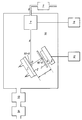
- FIG. 1 is a schematic view of apparatus for carrying out a method of depositing a superconducting film according to the invention.
- FIG. 1 A diagram of the deposition apparatus is shown in Figure 1 and used to give the following detailed description of the formation of Y1Ba2Cu3O 7- ⁇ thin films from a target of composition Y1Ba2Cu3O 7- ⁇ .
- a Y1Ba2Cu3O 7- ⁇ ceramic target (2) mounted on a water cooled base (1), is positioned so that an ion beam (6) from an ion gun (7) impinges the target (2) centrally and at an angle ⁇ to the target normal.
- a substrate (4) is mounted on a substrate heater (5) and positioned a distance d from the target (2) at an angle ⁇ to it, such that the correct geometry is achieved for the material sputtered from the target by the ion beam to impinge on the substrate (4).
- a deposition chamber (10) is evacuated by a LN2 cooled diffusion pump (13) backed by a rotary pump (14).
- Argon (8) controlled by a mass flow control system (9) is introduced into the chamber at the required pressure through the ion gun (7).
- a shutter (3) is placed across the substrate (4) to allow precleaning of the target (2) by the ion beam (6).
- the ion beam (6) is adjusted to the required power levels using power supply (11).
- Once the target is clean the substrate is heated to the required deposition temperature by heater (5) and control electronics (12).
- the shutter (3) is removed from over the substrate (4) to enable deposition to commence.
- the shutter (3) is replaced over the substrate (4) at the d the deposition.
- a post-deposition anneal of the Y1Ba2Cu3O 7- ⁇ film may be required to form the superconducting phase.
- Typical deposition conditions are given in Table 1.
- Table 1 Typical Deposition Conditions
- Deposition pressure 1.10-4 - 4.10-4 torr
- Substrate temperature 0 - 1000°C
- the ion beam gun may be replaced by a fast atomic beam gun.
- a further fast atomic beam or ion beams may be included to enable pre-cleaning of the substrate and surface stimulation of the growing film during deposition.
- Inert gases other than argon may be employed to produce the ion beam.
- Oxygen may be introduced into the system, either with the inert gas or independently, for example at the substrate surface.
Landscapes
- Chemical & Material Sciences (AREA)
- Engineering & Computer Science (AREA)
- Organic Chemistry (AREA)
- Materials Engineering (AREA)
- Mechanical Engineering (AREA)
- Metallurgy (AREA)
- Chemical Kinetics & Catalysis (AREA)
- Manufacturing & Machinery (AREA)
- Superconductors And Manufacturing Methods Therefor (AREA)
- Superconductor Devices And Manufacturing Methods Thereof (AREA)
- Inorganic Compounds Of Heavy Metals (AREA)
- Oxygen, Ozone, And Oxides In General (AREA)
- Physical Vapour Deposition (AREA)
Applications Claiming Priority (2)
| Application Number | Priority Date | Filing Date | Title |
|---|---|---|---|
| GB8728970A GB2213501A (en) | 1987-12-11 | 1987-12-11 | Production of superconducting thin films by ion beam sputtering from a single ceramic target |
| GB8728970 | 1987-12-11 |
Publications (1)
| Publication Number | Publication Date |
|---|---|
| EP0321071A1 true EP0321071A1 (de) | 1989-06-21 |
Family
ID=10628362
Family Applications (1)
| Application Number | Title | Priority Date | Filing Date |
|---|---|---|---|
| EP88308479A Withdrawn EP0321071A1 (de) | 1987-12-11 | 1988-09-14 | Methode zur Herstellung supraleitender Dünnschichten |
Country Status (3)
| Country | Link |
|---|---|
| EP (1) | EP0321071A1 (de) |
| JP (1) | JPH01208464A (de) |
| GB (1) | GB2213501A (de) |
Citations (1)
| Publication number | Priority date | Publication date | Assignee | Title |
|---|---|---|---|---|
| EP0280322A2 (de) * | 1987-02-26 | 1988-08-31 | Sumitomo Electric Industries Limited | In Schichten angeordneter keramischer Supraleiter |
Family Cites Families (12)
| Publication number | Priority date | Publication date | Assignee | Title |
|---|---|---|---|---|
| NL296188A (de) * | 1962-08-02 | |||
| DE1515318A1 (de) * | 1964-12-28 | 1969-07-31 | Hermsdorf Keramik Veb | Einrichtung zur Herstellung duenner Schichten auf einem Traeger mittels Ionenstrahl-Zerstaeubung |
| US3549416A (en) * | 1965-06-01 | 1970-12-22 | Gulf Energy & Environ Systems | Process for forming superconductive materials |
| US3472751A (en) * | 1965-06-16 | 1969-10-14 | Ion Physics Corp | Method and apparatus for forming deposits on a substrate by cathode sputtering using a focussed ion beam |
| GB1057119A (en) * | 1965-11-16 | 1967-02-01 | Hermsdorf Keramik Veb | Method of and apparatus for the production of thin films on a substrate or carrier by ion beam sputtering |
| US3641402A (en) * | 1969-12-30 | 1972-02-08 | Ibm | Semiconductor device with beta tantalum-gold composite conductor metallurgy |
| ZA711702B (en) * | 1970-03-20 | 1971-12-29 | Whittaker Corp | Film deposition |
| US4713157A (en) * | 1976-02-17 | 1987-12-15 | Ramtron Corporation | Combined integrated circuit/ferroelectric memory device, and ion beam methods of constructing same |
| US4108751A (en) * | 1977-06-06 | 1978-08-22 | King William J | Ion beam implantation-sputtering |
| US4250009A (en) * | 1979-05-18 | 1981-02-10 | International Business Machines Corporation | Energetic particle beam deposition system |
| US4426268A (en) * | 1983-07-12 | 1984-01-17 | The United States Of America As Represented By The Secretary Of The Navy | Method for forming high superconducting Tc niobium nitride film at ambient temperatures |
| JPS61183979A (ja) * | 1985-02-08 | 1986-08-16 | Yoshiro Saji | 超電導磁気遮蔽体 |
-
1987
- 1987-12-11 GB GB8728970A patent/GB2213501A/en not_active Withdrawn
-
1988
- 1988-09-14 EP EP88308479A patent/EP0321071A1/de not_active Withdrawn
- 1988-12-09 JP JP63311799A patent/JPH01208464A/ja active Pending
Patent Citations (1)
| Publication number | Priority date | Publication date | Assignee | Title |
|---|---|---|---|---|
| EP0280322A2 (de) * | 1987-02-26 | 1988-08-31 | Sumitomo Electric Industries Limited | In Schichten angeordneter keramischer Supraleiter |
Non-Patent Citations (3)
| Title |
|---|
| JAPANESE JOURNAL OF APPLIED PHYSICS, vol. 20, supplement 20-4, 1981, pages 13-16, Tokyo, JP; M. SUZUKI et al.: "Thin film preparation of superconducting perovskite-type oxides by rf sputtering" * |
| JAPANESE JOURNAL OF APPLIED PHYSICS, vol. 26, no. 7, July 1987, pages L1199-1201, Tokyo, JP; O. MICHIKAMI et al.: "Synthesis of Y-Ba-Cu-O thin films on sapphire substrates by RF magnetron sputtering" * |
| JAPANESE JOURNAL OF APPLIED PHYSICS, vol. 26, no. 7, July 1987, pages L1221-L1222, Tokyo, JP; H. ASANO et al.: "High Tc Y-Ba-Cu-O thin film prepared by dual magnetron sputtering" * |
Also Published As
| Publication number | Publication date |
|---|---|
| GB2213501A (en) | 1989-08-16 |
| GB8728970D0 (en) | 1988-01-27 |
| JPH01208464A (ja) | 1989-08-22 |
Similar Documents
| Publication | Publication Date | Title |
|---|---|---|
| US6214772B1 (en) | Process for preparing polycrystalline thin film, process for preparing oxide superconductor, and apparatus therefor | |
| EP0302506B1 (de) | Verfahren und Vorrichtung zur Herstellung supraleitender Dünnschichten | |
| EP0309294A2 (de) | Verfahren und Vorrichtung zur Herstellung von supraleitenden Oxidmaterialien | |
| US5047385A (en) | Method of forming superconducting YBa2 Cu3 O7-x thin films with controlled crystal orientation | |
| US3887451A (en) | Method for sputtering garnet compound layer | |
| US4874741A (en) | Non-enhanced laser evaporation of oxide superconductors | |
| Raven | Radio frequency sputtering and the deposition of high-temperature superconductors | |
| US5061684A (en) | Production of thin layers of a high temperature superconductor (htsc) by a plasma-activated physical vapor deposition process, and cathodes used therein | |
| US5361720A (en) | Epitaxial deposition | |
| EP0321071A1 (de) | Methode zur Herstellung supraleitender Dünnschichten | |
| EP0631332B1 (de) | Verfahren zum Herstellen einer Y-Ba-Cu-O supraleitenden Dünnschicht | |
| JPH05116940A (ja) | 基板上に金属酸化物の薄膜を生成させる方法 | |
| EP0412986B1 (de) | Epitaktische abscheidung | |
| Shah et al. | Growth of YBa2Cu3O70 x thin films by sputtering | |
| Schneider et al. | Structural and electrical properties of DC bias sputtered YBaCuO films | |
| Acosta et al. | Influence of the sputtering variables in the ion bombardment during off-axis deposition of YBa 2 Cu 3 O x films | |
| EP0323003A2 (de) | Supraleitende Dünnschichten | |
| EP0412007A2 (de) | Verfahren zur Herstellung eines dünnen supraleitenden Films | |
| JP2523785B2 (ja) | 超電導体薄膜の製造方法 | |
| Agarwal et al. | A new approach for the preparation of in situ superconducting BSCCO films | |
| Manic et al. | Preparation of stoichiometric Bi–Sr–Ca–Cu–O superconducting thin films by RF diode sputtering | |
| Kingon et al. | YBa2Cu3O7− δ films deposited by a novel ion beam sputtering technique | |
| Lin et al. | Insulator-coated sputter gun for growing superconducting oxide films | |
| Kellett et al. | Ion beam sputter deposition of YBa2Cu3O7− δ thin films | |
| JP2505849B2 (ja) | 超電導セラミックス薄膜の製法 |
Legal Events
| Date | Code | Title | Description |
|---|---|---|---|
| PUAI | Public reference made under article 153(3) epc to a published international application that has entered the european phase |
Free format text: ORIGINAL CODE: 0009012 |
|
| AK | Designated contracting states |
Kind code of ref document: A1 Designated state(s): DE FR GB IT NL |
|
| STAA | Information on the status of an ep patent application or granted ep patent |
Free format text: STATUS: THE APPLICATION IS DEEMED TO BE WITHDRAWN |
|
| 18D | Application deemed to be withdrawn |
Effective date: 19891222 |