EP0280322A2 - In Schichten angeordneter keramischer Supraleiter - Google Patents
In Schichten angeordneter keramischer Supraleiter Download PDFInfo
- Publication number
- EP0280322A2 EP0280322A2 EP88102899A EP88102899A EP0280322A2 EP 0280322 A2 EP0280322 A2 EP 0280322A2 EP 88102899 A EP88102899 A EP 88102899A EP 88102899 A EP88102899 A EP 88102899A EP 0280322 A2 EP0280322 A2 EP 0280322A2
- Authority
- EP
- European Patent Office
- Prior art keywords
- ceramic superconductor
- laminated ceramic
- 2cuo4
- superconductor
- layer
- Prior art date
- Legal status (The legal status is an assumption and is not a legal conclusion. Google has not performed a legal analysis and makes no representation as to the accuracy of the status listed.)
- Withdrawn
Links
Images
Classifications
-
- H—ELECTRICITY
- H10—SEMICONDUCTOR DEVICES; ELECTRIC SOLID-STATE DEVICES NOT OTHERWISE PROVIDED FOR
- H10N—ELECTRIC SOLID-STATE DEVICES NOT OTHERWISE PROVIDED FOR
- H10N60/00—Superconducting devices
- H10N60/80—Constructional details
- H10N60/85—Superconducting active materials
-
- H—ELECTRICITY
- H10—SEMICONDUCTOR DEVICES; ELECTRIC SOLID-STATE DEVICES NOT OTHERWISE PROVIDED FOR
- H10N—ELECTRIC SOLID-STATE DEVICES NOT OTHERWISE PROVIDED FOR
- H10N60/00—Superconducting devices
- H10N60/20—Permanent superconducting devices
- H10N60/203—Permanent superconducting devices comprising high-Tc ceramic materials
-
- Y—GENERAL TAGGING OF NEW TECHNOLOGICAL DEVELOPMENTS; GENERAL TAGGING OF CROSS-SECTIONAL TECHNOLOGIES SPANNING OVER SEVERAL SECTIONS OF THE IPC; TECHNICAL SUBJECTS COVERED BY FORMER USPC CROSS-REFERENCE ART COLLECTIONS [XRACs] AND DIGESTS
- Y10—TECHNICAL SUBJECTS COVERED BY FORMER USPC
- Y10S—TECHNICAL SUBJECTS COVERED BY FORMER USPC CROSS-REFERENCE ART COLLECTIONS [XRACs] AND DIGESTS
- Y10S428/00—Stock material or miscellaneous articles
- Y10S428/922—Static electricity metal bleed-off metallic stock
- Y10S428/9265—Special properties
- Y10S428/93—Electric superconducting
-
- Y—GENERAL TAGGING OF NEW TECHNOLOGICAL DEVELOPMENTS; GENERAL TAGGING OF CROSS-SECTIONAL TECHNOLOGIES SPANNING OVER SEVERAL SECTIONS OF THE IPC; TECHNICAL SUBJECTS COVERED BY FORMER USPC CROSS-REFERENCE ART COLLECTIONS [XRACs] AND DIGESTS
- Y10—TECHNICAL SUBJECTS COVERED BY FORMER USPC
- Y10S—TECHNICAL SUBJECTS COVERED BY FORMER USPC CROSS-REFERENCE ART COLLECTIONS [XRACs] AND DIGESTS
- Y10S505/00—Superconductor technology: apparatus, material, process
- Y10S505/70—High TC, above 30 k, superconducting device, article, or structured stock
- Y10S505/701—Coated or thin film device, i.e. active or passive
- Y10S505/702—Josephson junction present
-
- Y—GENERAL TAGGING OF NEW TECHNOLOGICAL DEVELOPMENTS; GENERAL TAGGING OF CROSS-SECTIONAL TECHNOLOGIES SPANNING OVER SEVERAL SECTIONS OF THE IPC; TECHNICAL SUBJECTS COVERED BY FORMER USPC CROSS-REFERENCE ART COLLECTIONS [XRACs] AND DIGESTS
- Y10—TECHNICAL SUBJECTS COVERED BY FORMER USPC
- Y10S—TECHNICAL SUBJECTS COVERED BY FORMER USPC CROSS-REFERENCE ART COLLECTIONS [XRACs] AND DIGESTS
- Y10S505/00—Superconductor technology: apparatus, material, process
- Y10S505/70—High TC, above 30 k, superconducting device, article, or structured stock
- Y10S505/704—Wire, fiber, or cable
- Y10S505/705—Magnetic coil
-
- Y—GENERAL TAGGING OF NEW TECHNOLOGICAL DEVELOPMENTS; GENERAL TAGGING OF CROSS-SECTIONAL TECHNOLOGIES SPANNING OVER SEVERAL SECTIONS OF THE IPC; TECHNICAL SUBJECTS COVERED BY FORMER USPC CROSS-REFERENCE ART COLLECTIONS [XRACs] AND DIGESTS
- Y10—TECHNICAL SUBJECTS COVERED BY FORMER USPC
- Y10T—TECHNICAL SUBJECTS COVERED BY FORMER US CLASSIFICATION
- Y10T428/00—Stock material or miscellaneous articles
- Y10T428/31504—Composite [nonstructural laminate]
- Y10T428/31678—Of metal
Definitions
- the present invention relates to a laminated superconductor. More particularly, it relates to a laminated superconductor comprising at least two layers of ceramic superconductor and a stabilizing metal layer interposed between said ceramic superconductor layers, which can be used as a flexible wire for connecting electrical or electric devices or as a conductive wire of a superconducting magnet.
- a metallic one As a superconductive material, a metallic one, a ceramic one and an organic compound type one are known.
- the ceramic superconductor such as one having a layer perovskite (K2NiF4) crystal structure has been found to have a higher critical temperature and is recently very actively studied and developed.
- an oxide type ceramic superconductor such as [LaSr]2CuO4 and [LaBa]2CuO4 has a critical temperature of higher then 30K.
- the ceramic superconductor is hard and brittle, and only a very thin film of ceramic superconductor has flexibility.
- the ceramic superconductor should be as thin as about 10 ⁇ m.
- such thin film ceramic superconductor cannot have a large critical current density.
- the ceramic superconductor is very brittle and its processing is not so easy as metal superconductors.
- One object of the present invention is to provide a laminated ceramic superconductor with improved flexibility.
- Another object of the present invention is to provide a laminated ceramic superconductor having good processability.
- Further object of the present invention is to provide a laminated ceramic superconductor having an increased critical current density.
- a laminated ceramic superconductor which comprises at least two layers of ceramic superconductor and a stabilizing metal layer interposed between said ceramic superconductor layers.
- any of known ceramic superconductors may be used. Particularly, those having a layer perovskite crystal structure are preferred.
- Preferred examples of the ceramic superconductors are those having a composition formula of (M1 x-1 M2 x )2M3M4 4-y (I) wherein M1 is an element selected from the lanthanum series elements, M2 is an element selected form the elements of the Ia, IIa and IIIa groups, M3 is an element selected from the group consisting of elements of Ib, IIb and IIIb groups and transition elements, M4 is an element selected from the group consisting of oxygen, boron, carbon, nitrogen, fluorine and sulfur, x is a number of larger than 0 (zero) and smaller than 1 (one), and y is a number of not smaller than 0 (zero) and smaller than 4.
- ceramic superconductor of the formula (I) are (La x-1 Sr x )2CuO4, (La x-1 Ba x )2CuO4, (Y x-1 Sr x )2CuO4 and (Y x-1 Ba x )2CuO4.
- the layer of ceramic superconductor can be formed by ion beam spattering, multi-element vacuum deposition, plasma CVD, plasma spray coating, and a sol-gel method. By these methods, the layer of ceramic superconductor is formed on the stabilizing metal layer without strain.
- the thickness of ceramic superconductor layer is from 0.1 to 100 ⁇ m, preferably from 1 to 50 ⁇ m.
- the stabilizing layer is formed by a conductive metal such as copper, aluminum, silver, gold and the like.
- the stabilizing metal layer may be supplied in the form of a thin foil or film or formed by any one of the methods which are used for forming the layer of ceramic superconductor.
- the thickness of the stabilizing metal layer is from 10 to 1,000 ⁇ m, preferably from 50 to 800 ⁇ m.
- Fig. 2 shows a cross section of one preferred embodiment of a laminated ceramic superconductor in the sheet form according to the present invention, which comprises a copper tape 1 as a center stabilizing layer, two ceramic superconductor layers 2,2 which sandwich the copper tape 1 and two outer stabilizing copper layers 3,3 formed on the outer surfaces of the respective ceramic superconductor layers 2,2.
- each ceramic superconductor layer was 0.01 mm.
- a stabilizing copper layer having a thickness of 0.02 mm was formed by sputtering under following conditions; Apparatus: DC magnetron sputtering apparatus Conditions: Temperature: Room temperature Pressure: 2 ⁇ 10 ⁇ 2 Torr. DC powder: 100 Watts Time: 25 minutes
- the produced laminated ceramic superconductor exhibited superconductivity stably at about 36K.
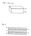
- Fig. 3 shows a perspective view of another preferivelyred embodiment of a sheet form laminated ceramic superconductor according to the present invention, which comprises three ceramic superconductor layers 11a,11b,11c each of which is made of a ceramic superconductor having a composition of YBa2Cu3O 6.8 and has a thickness of 10 ⁇ m and three stabilizing metal layers 12a,12b,12c each of which is made of copper and has a thickness of 100 ⁇ m.
- the laminated ceramic superconductor of Fig. 3 exhibited critical current of 30 A at 77K.
- a laminated ceramic superconductor having a structure shown in Fig. 1 was produced.
- Said two layer ceramic superconductor consisted of a ceramic superconductor layer 13 which was made of a ceramic superconductor having a composition of YBa2Cu3O 6.8 and had a thickness of 30 ⁇ m and a stabilizing copper layer 14 which had a thickness of 100 ⁇ m.
- the critical current of the comparative laminated ceramic superconductor was 10 A at 77K.
- Both laminated ceramic superconductors of Example 2 and Comparative Example could be bent to a radius of curvature of 1 cm without decrease of current capacity.
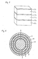
- the laminated ceramic superconductor of the present invention may be in the form of a wire as shown in Fig. 4, which comprises a core conductive metal wire 4 made of for example, aluminum, copper and the like, a ceramic superconductor layer 5, a stabilizing aluminum layer 6, a second super conductor layer 7, a stabilizing layer 8, a third ceramic superconductor layer 9 and a stablilizing layer 10.
Landscapes
- Chemical & Material Sciences (AREA)
- Engineering & Computer Science (AREA)
- Ceramic Engineering (AREA)
- Superconductors And Manufacturing Methods Therefor (AREA)
- Compositions Of Oxide Ceramics (AREA)
- Laminated Bodies (AREA)
- Inorganic Compounds Of Heavy Metals (AREA)
Applications Claiming Priority (4)
| Application Number | Priority Date | Filing Date | Title |
|---|---|---|---|
| JP44266/87 | 1987-02-26 | ||
| JP62044266A JP2567386B2 (ja) | 1987-02-26 | 1987-02-26 | 超電導導体 |
| JP62209932A JPS6454612A (en) | 1987-08-24 | 1987-08-24 | Superconductive structure |
| JP209932/87 | 1987-08-24 |
Publications (2)
| Publication Number | Publication Date |
|---|---|
| EP0280322A2 true EP0280322A2 (de) | 1988-08-31 |
| EP0280322A3 EP0280322A3 (de) | 1990-05-16 |
Family
ID=26384116
Family Applications (1)
| Application Number | Title | Priority Date | Filing Date |
|---|---|---|---|
| EP19880102899 Withdrawn EP0280322A3 (de) | 1987-02-26 | 1988-02-26 | In Schichten angeordneter keramischer Supraleiter |
Country Status (2)
| Country | Link |
|---|---|
| US (1) | US5151406A (de) |
| EP (1) | EP0280322A3 (de) |
Cited By (4)
| Publication number | Priority date | Publication date | Assignee | Title |
|---|---|---|---|---|
| EP0321071A1 (de) * | 1987-12-11 | 1989-06-21 | Plessey Overseas Limited | Methode zur Herstellung supraleitender Dünnschichten |
| EP0282839A3 (en) * | 1987-03-18 | 1990-07-25 | International Business Machines Corporation | Films of high tc oxide superconductors and method for making the same |
| EP0581366A1 (de) * | 1992-07-28 | 1994-02-02 | CISE S.p.A. | Verfahren zur Herstellung eines elektrischen Koaxialkabels mit keramischem Hochtemperatur-Supraleitermaterial |
| EP0393932B1 (de) * | 1989-04-17 | 1995-04-05 | Ngk Insulators, Ltd. | Supraleitende Struktur zur magnetischen Abschirmung |
Families Citing this family (16)
| Publication number | Priority date | Publication date | Assignee | Title |
|---|---|---|---|---|
| EP0505015B1 (de) * | 1987-03-13 | 1997-05-14 | Kabushiki Kaisha Toshiba | Supraleitender Draht und Verfahren zu seiner Herstellung |
| CA2063282C (en) * | 1991-03-20 | 1998-05-19 | Hidehito Mukai | High temperature superconducting wire using oxide superconductive material |
| US5479059A (en) * | 1993-08-23 | 1995-12-26 | United Technologies Corporation | Thin film superconductor magnetic bearings |
| US5830828A (en) | 1994-09-09 | 1998-11-03 | Martin Marietta Energy Systems, Inc. | Process for fabricating continuous lengths of superconductor |
| US6034324A (en) * | 1995-09-12 | 2000-03-07 | Bwx Technology, Inc. | Modular high temperature superconducting down lead with safety lead |
| US5801124A (en) * | 1996-08-30 | 1998-09-01 | American Superconductor Corporation | Laminated superconducting ceramic composite conductors |
| US5987342A (en) * | 1996-08-30 | 1999-11-16 | American Superconductor Corporation | Laminated superconducting ceramic tape |
| US6110606A (en) | 1996-08-30 | 2000-08-29 | American Superconductor Corporation | Cryogen protected superconducting ceramic tape |
| US6370405B1 (en) | 1997-07-29 | 2002-04-09 | American Superconductor Corporation | Fine uniform filament superconductors |
| GB9805646D0 (en) * | 1998-03-18 | 1998-05-13 | Bicc Plc | Superconducting tapes |
| GB9805639D0 (en) * | 1998-03-18 | 1998-05-13 | Metal Manufactures Ltd | Superconducting tapes for alternating current and cables and other conductors in which they are used |
| GB9805644D0 (en) * | 1998-03-18 | 1998-05-13 | Metal Manufactures Ltd | Superconducting tapes |
| GB9805641D0 (en) * | 1998-03-18 | 1998-05-13 | Metal Manufactures Ltd | Superconducting tapes |
| US6253096B1 (en) * | 1999-07-08 | 2001-06-26 | The University Of Chicago | Shielded high-TC BSCCO tapes or wires for high field applications |
| US6444917B1 (en) | 1999-07-23 | 2002-09-03 | American Superconductor Corporation | Encapsulated ceramic superconductors |
| US7162286B2 (en) * | 2003-07-03 | 2007-01-09 | Superpower, Inc. | Superconducting articles, and methods for forming and using same |
Family Cites Families (3)
| Publication number | Priority date | Publication date | Assignee | Title |
|---|---|---|---|---|
| FR1479481A (fr) * | 1966-03-23 | 1967-05-05 | Comp Generale Electricite | Câble supraconducteur |
| US3625662A (en) * | 1970-05-18 | 1971-12-07 | Brunswick Corp | Superconductor |
| DE3524082A1 (de) * | 1985-07-05 | 1987-01-08 | Bbc Brown Boveri & Cie | Supraleitende faser und verfahren zu deren herstellung |
-
1988
- 1988-02-25 US US07/160,115 patent/US5151406A/en not_active Expired - Fee Related
- 1988-02-26 EP EP19880102899 patent/EP0280322A3/de not_active Withdrawn
Cited By (6)
| Publication number | Priority date | Publication date | Assignee | Title |
|---|---|---|---|---|
| EP0282839A3 (en) * | 1987-03-18 | 1990-07-25 | International Business Machines Corporation | Films of high tc oxide superconductors and method for making the same |
| EP0662724A3 (de) * | 1987-03-18 | 1995-08-09 | Ibm | |
| US5447906A (en) * | 1987-03-18 | 1995-09-05 | International Business Machines Corporation | Thin film high TC oxide superconductors and vapor deposition methods for making the same |
| EP0321071A1 (de) * | 1987-12-11 | 1989-06-21 | Plessey Overseas Limited | Methode zur Herstellung supraleitender Dünnschichten |
| EP0393932B1 (de) * | 1989-04-17 | 1995-04-05 | Ngk Insulators, Ltd. | Supraleitende Struktur zur magnetischen Abschirmung |
| EP0581366A1 (de) * | 1992-07-28 | 1994-02-02 | CISE S.p.A. | Verfahren zur Herstellung eines elektrischen Koaxialkabels mit keramischem Hochtemperatur-Supraleitermaterial |
Also Published As
| Publication number | Publication date |
|---|---|
| EP0280322A3 (de) | 1990-05-16 |
| US5151406A (en) | 1992-09-29 |
Similar Documents
| Publication | Publication Date | Title |
|---|---|---|
| EP0280322A2 (de) | In Schichten angeordneter keramischer Supraleiter | |
| US4994435A (en) | Laminated layers of a substrate, noble metal, and interlayer underneath an oxide superconductor | |
| EP0292959B1 (de) | Supraleitendes Element | |
| EP0430737B1 (de) | Eine supraleitende Dünnschicht | |
| US4866032A (en) | Method and apparatus for producing thin film of high to superconductor compound having large area | |
| EP0327493B1 (de) | Epitaxische Anordnung von Hochtemperatur-Supraleitern | |
| CN1047418A (zh) | 隧道型约瑟夫森器件及其制造方法 | |
| JP2760994B2 (ja) | 超伝導性薄層 | |
| US5428005A (en) | Superconducting thin film of compound oxide and a process of preparing the same | |
| EP1479111A1 (de) | Verbesserter supraleiter und deren herstellungsverfahren | |
| EP0466611A1 (de) | Schichtkörper umfassend ein Siliziumsubstrat und supraleitende Dünnfilmschichten | |
| EP0427640A1 (de) | Tunnelübergangsanordnung mit supraleitendem Oxydverbundmaterial | |
| EP0325877A1 (de) | Halbleitersubstrat mit einem supraleitenden Dünnfilm | |
| EP0342038B1 (de) | Josephson-Einrichtung | |
| EP0341148A2 (de) | Halbleitersubstrat mit dünner Supraleiterschicht | |
| JPH03259576A (ja) | ジョセフソン接合 | |
| EP0347336B1 (de) | Verfahren zur Abscheidung einer dünnen Supraleiterschicht | |
| WO2006036547A2 (en) | Methods for forming superconducting conductors | |
| US5296458A (en) | Epitaxy of high Tc superconducting films on (001) silicon surface | |
| EP0357500B1 (de) | Verfahren zum Herstellen einer supraleitenden Dünnschicht vom Wismut-Typ | |
| EP0508893A1 (de) | Substrat für einen Mikrowellenbauteil | |
| CA2008310C (en) | Superconducting wire | |
| EP0461592B1 (de) | Dünnschicht Josephson-Vorrichtung | |
| US7781377B2 (en) | Anti-epitaxial film in a superconducting article and related articles, devices and systems | |
| EP0519769B1 (de) | Verfahren zur Herstellung einer supraleitenden Dünnschicht aus einer oxidverbindung |
Legal Events
| Date | Code | Title | Description |
|---|---|---|---|
| PUAI | Public reference made under article 153(3) epc to a published international application that has entered the european phase |
Free format text: ORIGINAL CODE: 0009012 |
|
| AK | Designated contracting states |
Kind code of ref document: A2 Designated state(s): DE FR GB IT |
|
| PUAL | Search report despatched |
Free format text: ORIGINAL CODE: 0009013 |
|
| AK | Designated contracting states |
Kind code of ref document: A3 Designated state(s): DE FR GB IT |
|
| RHK1 | Main classification (correction) |
Ipc: H01L 39/14 |
|
| 17P | Request for examination filed |
Effective date: 19900711 |
|
| 17Q | First examination report despatched |
Effective date: 19921027 |
|
| STAA | Information on the status of an ep patent application or granted ep patent |
Free format text: STATUS: THE APPLICATION IS DEEMED TO BE WITHDRAWN |
|
| 18D | Application deemed to be withdrawn |
Effective date: 19930309 |