EP0320714B1 - Einrichtungen zur Paketvermittlung - Google Patents
Einrichtungen zur Paketvermittlung Download PDFInfo
- Publication number
- EP0320714B1 EP0320714B1 EP88120125A EP88120125A EP0320714B1 EP 0320714 B1 EP0320714 B1 EP 0320714B1 EP 88120125 A EP88120125 A EP 88120125A EP 88120125 A EP88120125 A EP 88120125A EP 0320714 B1 EP0320714 B1 EP 0320714B1
- Authority
- EP
- European Patent Office
- Prior art keywords
- packet
- subpackets
- packets
- switching
- memory
- Prior art date
- Legal status (The legal status is an assumption and is not a legal conclusion. Google has not performed a legal analysis and makes no representation as to the accuracy of the status listed.)
- Expired - Lifetime
Links
Images


Classifications
-
- H—ELECTRICITY
- H04—ELECTRIC COMMUNICATION TECHNIQUE
- H04L—TRANSMISSION OF DIGITAL INFORMATION, e.g. TELEGRAPHIC COMMUNICATION
- H04L49/00—Packet switching elements
- H04L49/30—Peripheral units, e.g. input or output ports
- H04L49/3009—Header conversion, routing tables or routing tags
-
- H—ELECTRICITY
- H04—ELECTRIC COMMUNICATION TECHNIQUE
- H04L—TRANSMISSION OF DIGITAL INFORMATION, e.g. TELEGRAPHIC COMMUNICATION
- H04L12/00—Data switching networks
- H04L12/64—Hybrid switching systems
-
- H—ELECTRICITY
- H04—ELECTRIC COMMUNICATION TECHNIQUE
- H04L—TRANSMISSION OF DIGITAL INFORMATION, e.g. TELEGRAPHIC COMMUNICATION
- H04L49/00—Packet switching elements
- H04L49/15—Interconnection of switching modules
- H04L49/1553—Interconnection of ATM switching modules, e.g. ATM switching fabrics
- H04L49/1561—Distribute and route fabrics, e.g. Batcher-Banyan
-
- H—ELECTRICITY
- H04—ELECTRIC COMMUNICATION TECHNIQUE
- H04L—TRANSMISSION OF DIGITAL INFORMATION, e.g. TELEGRAPHIC COMMUNICATION
- H04L49/00—Packet switching elements
- H04L49/30—Peripheral units, e.g. input or output ports
- H04L49/3072—Packet splitting
-
- H—ELECTRICITY
- H04—ELECTRIC COMMUNICATION TECHNIQUE
- H04L—TRANSMISSION OF DIGITAL INFORMATION, e.g. TELEGRAPHIC COMMUNICATION
- H04L49/00—Packet switching elements
- H04L49/30—Peripheral units, e.g. input or output ports
- H04L49/3081—ATM peripheral units, e.g. policing, insertion or extraction
-
- H—ELECTRICITY
- H04—ELECTRIC COMMUNICATION TECHNIQUE
- H04L—TRANSMISSION OF DIGITAL INFORMATION, e.g. TELEGRAPHIC COMMUNICATION
- H04L49/00—Packet switching elements
- H04L49/60—Software-defined switches
- H04L49/606—Hybrid ATM switches, e.g. ATM&STM, ATM&Frame Relay or ATM&IP
-
- H—ELECTRICITY
- H04—ELECTRIC COMMUNICATION TECHNIQUE
- H04L—TRANSMISSION OF DIGITAL INFORMATION, e.g. TELEGRAPHIC COMMUNICATION
- H04L12/00—Data switching networks
- H04L12/54—Store-and-forward switching systems
- H04L12/56—Packet switching systems
- H04L12/5601—Transfer mode dependent, e.g. ATM
- H04L2012/5638—Services, e.g. multimedia, GOS, QOS
- H04L2012/5646—Cell characteristics, e.g. loss, delay, jitter, sequence integrity
- H04L2012/5652—Cell construction, e.g. including header, packetisation, depacketisation, assembly, reassembly
- H04L2012/566—Cell construction, e.g. including header, packetisation, depacketisation, assembly, reassembly using the ATM layer
- H04L2012/5662—Macrocells or frames
Definitions
- the invention relates to a packet switching device, an input unit therefor and an output unit therefor.
- Messages with statistical traffic are preferably transmitted in packets with packets of equal length to one another via virtual connections. It is currently assumed that the messages with deterministic traffic volume are transmitted in the same way and together with the others.
- Buffer memories must therefore be provided in which those packets that cannot be immediately forwarded can wait.
- the storage effort required for this depends, apart from the length of the packets, in particular on the number of lines coming together, on the type of traffic volume and on the required traffic quality. In known packet switching devices, about 80% of all chip areas are used for this memory within the switching matrix.
- the invention has for its object to provide a packet switching device that requires significantly less memory with comparable performance.
- a fixed number of packets is combined into a frame within the switching device, and all packets are broken down into packet parts of equal length and divided into subframes.
- Mediation is based on subframes in synchronous time division multiplexing.
- the space requirement in the coupling network is reduced in the frame: subframe ratio.
- the memories that are required anyway in the case of synchronous time division multiplex switching act primarily as memories. An additional storage effect can be achieved if additional empty packets are inserted at the inputs and clocked faster within the switching device.
- the PRELUDE project of the CNET (Center National d'Etudes des Telecommunications) in France is one of the first and best-known switching centers for fast packet switching.
- a description can be found, for example, in IEEE International Conference on Communications '87, vol. 2, June 1987, IEEE New York US, pages 769-773; J. Coudreuse et al .: "PRELUDE: AN ASYNCHRONOUS TIME-DIVISION SWITCHED NETWORK".
- the incoming packets are actually also divided into a number of packet parts, which are then switched to the exit of the switching center.
- a super multiplexing takes place on the input side; that is, the message streams of all inputs are combined into a single message stream.
- This super multiplex message stream is written into a buffer, read out again in a different order and distributed to the various outputs by demultiplexing.
- the packet parts of a packet are distributed over different lines in the manner of parallel processing (here, however, staggered in time). Larger, multi-level exchanges can hardly be realized in this way.
- Such externally specified frames are advantageously adopted within the switching facility. Without additional measures, messages whose packets recur periodically within the frame are then routed with their advantages (no delay jitter and no losses).
- the invention is described in terms which are primarily applied to spatially concentrated switching devices.
- the following exemplary embodiment also represents a concentrated switching device.
- the present invention is equally equally suitable for non-concentrated ones Switching devices, for example ring systems, can be used.
- Switching devices for example ring systems
- reference is made on the one hand to the already mentioned article from "Der Fernmelde Ingenieur”, where bus and ring systems under 4.1.2 are subordinate to the coupling arrangements under 4, and on the other hand to the publication EP-A2-0 125 744, "Closed loop telecommunication system ", in which a ring system is described in which a complete frame with a large number of packets always rotates, for which purpose shift registers or other memories are required.
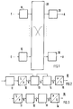
- a switching device As FIG. 1 shows, a switching device according to the invention initially, like any other switching device, has a plurality of inputs E, a plurality of outputs A and a switching network 20. According to the invention, an input unit 10 is now inserted between each input E and the coupling network 20 and an output unit 30 is inserted between the coupling network 20 and each output A.
- FIG. 2 now shows an input unit 10 according to the invention in further detail. It has a synchronization device 11, a series-parallel converter 12, a brand corrector 13, an input sorter 14 and a parallel-series converter 15.
- the synchronization device 11 recognizes the clocks contained in the input data stream, in particular the bit clock and the beginnings of the incoming packets. If the external data stream already has a frame clock, this can be adopted. Otherwise a fixed number of packages, e.g. 70, combined into a frame. Even if there is an outer frame clock, the inner one can differ. However, a synchronous transmission process for individual messages is not always guaranteed.
- the series-parallel converter 12 converts the data stream octet-wise, ie 8 bits each, into a parallel data stream.
- the synchronization required for this by the synchronization device 11 is not shown in FIG. 2.
- the brand corrector 13 first changes the format of the individual packages. Each package consists of an information part (payload) and a preceding label (header, label). The brand is information for the next exchange, the incoming brand is therefore initially replaced by an outgoing brand. In addition, there is an internal brand that contains priority information (e.g. ATM, STM), route information and information about the internal meaning (e.g. tax package, empty package). In addition, at least for ATM packets, there is a marker for the end of the packet. Due to the additional information, the bit clock is increased in the mark corrector 13. Phase fluctuations between internal and external clock can therefore also be compensated for here. At this point, the repetition frequency of the packets (packet cycle) can be increased without any problems. For this purpose, additional empty packets are added, which act like additional buffer memories within the switching network 20.
- the input sorter 14 receives from the mark corrector 13 on the one hand the packets in internal format and on the other hand the packet clock and clocks derived therefrom (octet clock, bit clock). Each parcel is broken down into a predetermined number of parcel parts of equal length. The parcel parts of the various parcels are now rearranged in such a way that subframes are created which contain a parcel part from each parcel, the associated parcel parts always being equally far apart. If, for example, 70 packets of 40 octets each are combined in a frame and each octet forms a packet part, after the re-sorting 70 octets form a subframe, each octet belonging to a different packet.
- the packet is then set up as for a circuit-switched connection through the first packet part, a connection through the switching network 20, which is then followed by the remaining packet parts.
- the connection is cleared again by the last part of a package. If a packet part is not sufficient for route information through the entire switching network, the connection must be set up in stages.
- the establishment of virtual connections proceeds in such a way that in a connection establishment phase the path that the packets coming later have to take is sketched out. This is done, for example, by using tables, e.g. in brand convertors, by means of which an incoming brand can be assigned to each incoming brand. This then defines the specific physical path, but not the point in time of the transfer.
- a specific time slot for the individual packet parts is now determined for each packet within the path already defined.
- a fixed time slot can be reserved for them in the predetermined way. This reservation can be made by not providing the last part of the package with end-of-package information.
- the parallel-serial converter 15 following the input sorter 14 converts the individual octets back into a serial packet flow.
- the output units 30 are constructed accordingly. They each have a series-parallel converter 31, an output sorter 32, a packet format converter 33 and a parallel-series converter 34.
- the output sorter 32 re-sorts the package parts in such a way that the package parts belonging to a package are combined again.
- the packet format converter 33 removes the internal marks and the end-of-packet marks. If 10 empty packets have been inserted in the input units, the same number of packets must now be removed again.
- all frames and subframes are synchronized with each other in each stage of the switching device and the first subframe of a frame contains all packet starts. Then, with the first subframe occurring everywhere at the same time in the entire switching network 20, the time slots are firmly allocated in the already predetermined ways for this and all subframes belonging to the same frame, this allocation being predetermined for STM connections and free for ATM connections. At the last subframe, all time slot allocations are then canceled again.
- the simplest way to always guarantee the same time slot allocation for STM connections is to not cancel this allocation at the end of a packet, which can be achieved by missing packet end information.
- This input sorter 14 works with a frame memory 141, which does not require more storage space than is required for exactly one frame, and with which it is nevertheless rearranged within the frame as required.
- the input sorter 14 consists essentially of the frame memory 141 and an addressing unit which contains a full adder 142, a register 143, a read-only memory (ROM) 144, a counter 145, a six-fold AND gate 146, a memory 147 and further gates 148a, 148b, 148c and 149.
- ROM read-only memory
- the task of the addressing unit comprises the conversion of the serial stream of packets into the synchronous time-division multiplex subframes with packet parts.
- N packets form a frame.
- the frame memory 141 contains n X m memory words for each packet part, where m indicates the number of packet parts per packet.
- the Frame memory 141 is numbered from 0 to (n X m-1).
- Each time division subframe contains a packet part of each packet of a frame.
- the order of the package parts in the subframe is the same as the order of the packages in the frame.
- the first subframe thus contains the first packet parts of all packets
- the second subframe contains the second packet parts of all packets, etc. Now a packet part is read out of the frame memory 141 and a new packet part is written into the freed memory space immediately thereafter.
- step size S k the frame memory must then be run through S k times until all memory locations have been addressed once. If the address range is exceeded, memory locations must be addressed by n X m - 1, which is done by adding the two's complement of n X m - 1. Only at the S k th pass exactly the end of the frame memory 141 is reached again. Then one frame is completely read out and the next is complete registered. With the next step size, a frame is then read out again and a frame is written.
- the memory locations 0 to 17 are therefore to be addressed in the frame memory 141.
- address 17 a frame has been completely processed; the next frame and thus the next step size must be passed to. If the address 17 is exceeded, then the frame memory 141 must be run through again with the same step size. For this purpose, the address must first be reduced by 17 in order to get back into the address range.
- the respective address is contained in register 143. It has five digits, with the digits A .... E, where A represents the most significant bit, E the least significant bit.
- the full adder 142 adds the current step size indicated by the read-only memory 144 to the content of the register 143. The result of the addition is again transferred to register 143 as a new address. The transfer into the register is initiated by a clock T, which also, via an OR gate 149, causes the full adder to add.
- the full adder 142 has a carry F.
- the respectively occurring Step sizes are determined once using the formula for S k and stored in the read-only memory 144.
- the outputs of the read-only memory 144 are deactivated via a negating enable input EN and, on the other hand, the outputs of the memory 147 are activated via the enable input EN.
- the two's complement of 17 contained in the memory 147 is therefore added to the content of the register 143, so that the content of the register 143 is then again at zero.
- the output sorters 32 in the output units 30 can also be constructed in exactly the same way as the input sorters 14.
- This output sorter 32 works with a memory 321, which requires as much storage space as is required for two frames (expanded by any additional empty packets). This example is based on an external frame with 70 packets of 40 octets.
- the output sorter 32 essentially consists of the memory 321, a control packet output unit 324 and an addressing unit, which have a cyclic enroll counter 322, a cyclic search counter 323a, a packet mark detector 323b, an overwrite detector 323c , an STM address memory 325a, a readout counter 325b, a write-in counter 325c, an ATM address memory 326a, an address comparator 326b, two counters 326c and 326d, an adder 327a, an STM detector 327b , a dummy packet inserter 328, two buffers 327c and 327d and a plurality of gates 326f, 326e and 327e.
- control packet output unit 324 The task of the control packet output unit 324 is to issue control packets separately. These control packages are fed directly to the control units.
- the task of the addressing unit comprises the conversion of the synchronous time-division multiplex subframe into the serial packet stream.
- the addressing unit reduces the packet format directly to the information part (payload) and the preceding mark (label) and at the same time the packet clock within the switching network is converted to the external packet clock.
- the STM packets are read out of the memory 321 in such a way that they always take up the same space in the frame for the duration of the connection.
- the write-in counter 322 is clocked by the internal packet partial clock and addresses in cyclic order all memory locations of the memory 321 into which the packet parts coming from the switching network are written.
- the search counter 323a is clocked at the same clock rate as the write-in counter 322 and addresses the memory locations of the memory 321 by one frame delay compared to the write-in counter 322.
- the memory 321 outputs the packet part addressed by the search counter 323a to the packet mark detector 323b.
- the packet mark detector 323b examines whether the addressed packet part is the first packet part of a packet and in this case differentiates whether it is an ATM, STM or a control packet.
- the addresses of the search counter 323a are also fed to the ATM and STM address memories (326a, 325a) and to the control packet output unit 324.
- the packet mark detector 323b When the packet mark detector 323b has recognized a first packet part of a packet, it applies a WRITE signal to the corresponding unit (324, 325a, 326a), which then takes over the address of the search counter 323a.
- the write-in counter 325c is clocked with the internal partial packet clock and cyclically addresses the STM address memory 325a with the addresses from 0 to 69 (+ additional empty packet number). If the packet mark detector 323b has recognized an STM connection, it applies a WRITE signal to the STM address memory 325a and this stores the address of the search counter 323a in the memory location, which is provided by the write-in counter 325c is addressed, a. Provided that 32 STM packet parts are only placed in the first 70 octets of the subframe from the last switching network stage before the output sorter, it can be guaranteed that the packets of an STM connection are always in the same place on the frame. This can be thought of as mapping the STM address entries in STM address memory 325a to the packets in the frame.
- the readout counter 325b is clocked with the external packet clock and cyclically addresses the STM address memory 325a with the read addresses 0 to 69.
- the STM address memory content addressed by the readout counter 325b is output to the STM detector 327b and in STM address memory 325a reset to 0.
- the STM detector 327b detects whether the read value is greater than 0. In the event that the value is greater than 0, the STM detector 327b blocks the buffer 327d (disable) and applies a logic 0 to the AND gate 327e and the OR gate 326e.
- Buffer 327c takes the address from STM detector 327b and passes it to adder 327a. Adder 327a first adds an offset to the address.
- the address at the adder output points to the first packet part of the label in the memory 321.
- the adder 327a receives the external partial packet clock and constantly adds the value 70 (+ number of additional empty packets) with this clock.
- the adder 327a addresses the last packet part of a packet, a new address is pending at its input, unless it is blocked by the AND gate 327e.
- the units 326a to 326f together form a modified FIFO memory.
- the ATM address memory 326a is addressed with the (write-in) counter 326c and the (read-out) counter 326d.
- a WRITE signal from packet mark detector 323b to ATM address memory 326a causes the address provided by search counter 323a to be stored in the memory location addressed by counter 326c.
- the counter 326c is incremented by the WRITE signal of the packet mark detector 323b and cyclically addresses the (e.g. 2 X 78) memory locations of the ATM address memory 326a.
- Counter 326d is clocked by an OR gate 326f.
- An input of the OR gate 326f is connected to the overwrite detector 323c. From the number of STM and ATM WRITE signals of the packet mark detector 323b per frame duration, the latter recognizes the overwriting of an as yet unissued ATM packet in the memory 321 by a new packet.
- Comparator 326b compares the counts of counter 326d and counter 326c and provides a logic 1 to OR gate 326e and AND gate 327e if the counts are equal. The comparator 326b thus indicates whether an ATM packet is entered in the ATM address memory 326a and blocks the incrementing of the readout counter if the counter readings are the same 326d. If the ATM address memory 326a is empty and the STM detector 327b does not detect an STM packet either, it places a logic 1 on the AND gate 327e and its output thus goes to logic 1. This locks the adder 327a and the empty packet insertion unit 328 outputs an empty packet.
Landscapes
- Engineering & Computer Science (AREA)
- Computer Networks & Wireless Communication (AREA)
- Signal Processing (AREA)
- Data Exchanges In Wide-Area Networks (AREA)
- Use Of Switch Circuits For Exchanges And Methods Of Control Of Multiplex Exchanges (AREA)
- Contacts (AREA)
- Oscillators With Electromechanical Resonators (AREA)
- Pretreatment Of Seeds And Plants (AREA)
- Water Treatment By Sorption (AREA)
- Packaging Of Special Articles (AREA)
- Orthopedics, Nursing, And Contraception (AREA)
- Developing Agents For Electrophotography (AREA)
- Packages (AREA)
Priority Applications (1)
| Application Number | Priority Date | Filing Date | Title |
|---|---|---|---|
| AT88120125T ATE97280T1 (de) | 1987-12-18 | 1988-12-02 | Einrichtungen zur paketvermittlung. |
Applications Claiming Priority (2)
| Application Number | Priority Date | Filing Date | Title |
|---|---|---|---|
| DE3742941 | 1987-12-18 | ||
| DE19873742941 DE3742941A1 (de) | 1987-12-18 | 1987-12-18 | Einrichtungen zur paketvermittlung |
Publications (3)
| Publication Number | Publication Date |
|---|---|
| EP0320714A2 EP0320714A2 (de) | 1989-06-21 |
| EP0320714A3 EP0320714A3 (de) | 1991-07-31 |
| EP0320714B1 true EP0320714B1 (de) | 1993-11-10 |
Family
ID=6342910
Family Applications (1)
| Application Number | Title | Priority Date | Filing Date |
|---|---|---|---|
| EP88120125A Expired - Lifetime EP0320714B1 (de) | 1987-12-18 | 1988-12-02 | Einrichtungen zur Paketvermittlung |
Country Status (12)
| Country | Link |
|---|---|
| US (1) | US4922487A (enExample) |
| EP (1) | EP0320714B1 (enExample) |
| JP (1) | JPH0728311B2 (enExample) |
| KR (1) | KR960004717B1 (enExample) |
| CN (1) | CN1009411B (enExample) |
| AT (1) | ATE97280T1 (enExample) |
| AU (1) | AU613123B2 (enExample) |
| CA (1) | CA1337362C (enExample) |
| DE (2) | DE3742941A1 (enExample) |
| ES (1) | ES2048190T3 (enExample) |
| MX (1) | MX170240B (enExample) |
| NO (1) | NO171480C (enExample) |
Families Citing this family (38)
| Publication number | Priority date | Publication date | Assignee | Title |
|---|---|---|---|---|
| US7058062B2 (en) * | 1986-09-16 | 2006-06-06 | Hitachi, Ltd. | Packet switching system having self-routing switches |
| US5043979A (en) | 1986-09-16 | 1991-08-27 | Hitachi, Ltd. | Time-division channel arrangement |
| US6005867A (en) | 1986-09-16 | 1999-12-21 | Hitachi, Ltd. | Time-division channel arrangement |
| DE3742939A1 (de) * | 1987-12-18 | 1989-07-06 | Standard Elektrik Lorenz Ag | Verfahren zur hybriden paketvermittlung und einrichtungen hierzu |
| GB8824972D0 (en) * | 1988-10-25 | 1988-11-30 | Plessey Telecomm | Time division switch |
| EP0401238B1 (en) * | 1988-12-24 | 1993-06-30 | BELL TELEPHONE MANUFACTURING COMPANY Naamloze Vennootschap | Communication switching system |
| ES2076389T3 (es) * | 1990-03-14 | 1995-11-01 | Alcatel Nv | Elemento de conmutacion de tipo amt con varios modos de funcionamiento y red de conmutacion que lo comprende. |
| DE4008080A1 (de) * | 1990-03-14 | 1991-09-19 | Standard Elektrik Lorenz Ag | Atm-vermittlungsstelle |
| WO1991015070A1 (en) * | 1990-03-22 | 1991-10-03 | Australian And Overseas Telecommunications Corporation Limited | Multicasting method for a telecommunications network |
| NL9000780A (nl) * | 1990-04-03 | 1991-11-01 | Nederland Ptt | Werkwijze en inrichting voor het doorschakelen van dataeenheden. |
| JP2993715B2 (ja) * | 1990-08-17 | 1999-12-27 | 株式会社日立製作所 | Atmスイッチおよびその制御方法 |
| JP2764865B2 (ja) * | 1990-08-20 | 1998-06-11 | 富士通株式会社 | Atm交換回路構成方式 |
| US5166926A (en) * | 1990-12-18 | 1992-11-24 | Bell Communications Research, Inc. | Packet address look-ahead technique for use in implementing a high speed packet switch |
| CA2059027C (en) * | 1991-01-08 | 1996-07-02 | Toshiya Aramaki | Switching system with time-stamped packet distribution input stage and packet sequencing output stage |
| GB9104712D0 (en) * | 1991-03-06 | 1991-04-17 | Plessey Telecomm | Switching arrangement and method |
| DE4108213A1 (de) * | 1991-03-14 | 1992-09-17 | Standard Elektrik Lorenz Ag | Optische vermittlungseinrichtung und schaltmodul dafuer |
| AU655308B2 (en) * | 1991-07-01 | 1994-12-15 | Telstra Corporation Limited | High speed switching architecture |
| CA2112664A1 (en) * | 1991-07-01 | 1993-01-21 | Douglas Follett | High speed switching architecture |
| JPH0522345A (ja) * | 1991-07-12 | 1993-01-29 | Hitachi Ltd | 最大転送単位の最適値管理決定方式 |
| EP0537382A1 (en) * | 1991-10-15 | 1993-04-21 | ALCATEL BELL Naamloze Vennootschap | Packet transfer control arrangement and related method |
| US5396490A (en) * | 1992-03-23 | 1995-03-07 | Motorola, Inc. | Packet reassembly method and apparatus |
| SE515177C2 (sv) * | 1992-06-01 | 2001-06-25 | Ericsson Telefon Ab L M | Kvadratisk väljararkitektur |
| US5440545A (en) * | 1993-08-02 | 1995-08-08 | Motorola, Inc. | Packet delivery system |
| DE4343588A1 (de) * | 1993-12-21 | 1995-06-22 | Sel Alcatel Ag | Verfahren und Einrichtung zur zufälligen Auswahl einer von N gleichen Einheiten, sowie Koppelelement, Koppelnetz und Vermittlungsstelle damit |
| GB9411894D0 (en) * | 1994-06-14 | 1994-08-03 | Northern Telecom Ltd | Communications system |
| GB2337663B (en) * | 1995-03-31 | 2000-02-16 | Inmarsat Ltd | Communication method and apparatus |
| GB9516777D0 (en) * | 1995-08-16 | 1995-10-18 | Int Computers Ltd | Network coupler |
| JPH11154954A (ja) | 1997-11-20 | 1999-06-08 | Hitachi Ltd | Atmスイッチ |
| US6167041A (en) * | 1998-03-17 | 2000-12-26 | Afanador; J. Abraham | Switch with flexible link list manager for handling ATM and STM traffic |
| US6721271B1 (en) * | 1999-02-04 | 2004-04-13 | Nortel Networks Limited | Rate-controlled multi-class high-capacity packet switch |
| CN100367730C (zh) | 2001-02-14 | 2008-02-06 | 克利尔斯皮德科技有限公司 | 一种互连系统 |
| US7346037B2 (en) | 2001-03-26 | 2008-03-18 | Lg Electronics Inc. | Method of transmitting or receiving a data packet in packet data communication system using hybrid automatic repeat request |
| KR100425253B1 (ko) * | 2001-04-18 | 2004-03-30 | 주식회사 현대시스콤 | 무선통신 시스템에서의 순방향 패킷 송수신 방법 |
| US6937606B2 (en) * | 2001-04-20 | 2005-08-30 | International Business Machines Corporation | Data structures for efficient processing of IP fragmentation and reassembly |
| EP1521497A3 (de) * | 2003-09-30 | 2006-05-31 | Alcatel | Universal-Vermittlungsstelle, Verfahren zum Durchführen einer Vermittlungsaufgabe, Eingangseinheit, Ausgangseinheit und Anschlusseinheit |
| US7535893B1 (en) * | 2003-12-05 | 2009-05-19 | Mahi Networks, Inc. | TDM services using a packet-switched fabric |
| CN101217452B (zh) * | 2007-01-05 | 2010-08-04 | 华为技术有限公司 | 一种通过分组交换网传输tdm业务的方法、装置和系统 |
| USD766700S1 (en) * | 2015-02-15 | 2016-09-20 | Iacobucci Hf Aerospaces S.P.A. | Closure |
Family Cites Families (6)
| Publication number | Priority date | Publication date | Assignee | Title |
|---|---|---|---|---|
| GB2139852B (en) * | 1983-05-13 | 1986-05-29 | Standard Telephones Cables Ltd | Data network |
| FR2589656B1 (fr) * | 1985-07-03 | 1987-12-11 | Servel Michel | Procede et dispositif de conversion de multitrame de canaux numeriques en multitrame de paquets |
| JPS6218155A (ja) * | 1985-07-17 | 1987-01-27 | Nec Corp | 回線/パケツト統合交換方式 |
| US4698802A (en) * | 1986-03-07 | 1987-10-06 | American Telephone And Telegraph Company And At&T Information Systems Inc. | Combined circuit and packet switching system |
| US4679190A (en) * | 1986-04-28 | 1987-07-07 | International Business Machines Corporation | Distributed voice-data switching on multi-stage interconnection networks |
| US4785446A (en) * | 1986-11-07 | 1988-11-15 | International Business Machines Corporation | Distributed bit switching of a multistage interconnection network |
-
1987
- 1987-12-18 DE DE19873742941 patent/DE3742941A1/de active Granted
-
1988
- 1988-12-02 AT AT88120125T patent/ATE97280T1/de not_active IP Right Cessation
- 1988-12-02 ES ES88120125T patent/ES2048190T3/es not_active Expired - Lifetime
- 1988-12-02 EP EP88120125A patent/EP0320714B1/de not_active Expired - Lifetime
- 1988-12-02 DE DE88120125T patent/DE3885583D1/de not_active Expired - Fee Related
- 1988-12-05 AU AU26526/88A patent/AU613123B2/en not_active Ceased
- 1988-12-14 NO NO885544A patent/NO171480C/no not_active IP Right Cessation
- 1988-12-14 MX MX014173A patent/MX170240B/es unknown
- 1988-12-15 CA CA000585953A patent/CA1337362C/en not_active Expired - Fee Related
- 1988-12-16 US US07/286,305 patent/US4922487A/en not_active Expired - Lifetime
- 1988-12-16 JP JP63318299A patent/JPH0728311B2/ja not_active Expired - Lifetime
- 1988-12-17 KR KR1019880016909A patent/KR960004717B1/ko not_active Expired - Fee Related
- 1988-12-17 CN CN88108703A patent/CN1009411B/zh not_active Expired
Also Published As
| Publication number | Publication date |
|---|---|
| EP0320714A3 (de) | 1991-07-31 |
| JPH0728311B2 (ja) | 1995-03-29 |
| NO171480B (no) | 1992-12-07 |
| CA1337362C (en) | 1995-10-17 |
| DE3885583D1 (de) | 1993-12-16 |
| DE3742941C2 (enExample) | 1989-11-16 |
| NO885544L (no) | 1989-06-19 |
| ATE97280T1 (de) | 1993-11-15 |
| NO171480C (no) | 1993-03-17 |
| NO885544D0 (no) | 1988-12-14 |
| JPH022767A (ja) | 1990-01-08 |
| CN1034648A (zh) | 1989-08-09 |
| CN1009411B (zh) | 1990-08-29 |
| ES2048190T3 (es) | 1994-03-16 |
| EP0320714A2 (de) | 1989-06-21 |
| KR890011250A (ko) | 1989-08-14 |
| KR960004717B1 (ko) | 1996-04-12 |
| AU613123B2 (en) | 1991-07-25 |
| MX170240B (es) | 1993-08-12 |
| US4922487A (en) | 1990-05-01 |
| DE3742941A1 (de) | 1989-07-06 |
| AU2652688A (en) | 1989-06-22 |
Similar Documents
| Publication | Publication Date | Title |
|---|---|---|
| EP0320714B1 (de) | Einrichtungen zur Paketvermittlung | |
| DE3742939A1 (de) | Verfahren zur hybriden paketvermittlung und einrichtungen hierzu | |
| DE69020578T2 (de) | Grundelement für ein verbindungsnetzwerk eines knotens zur schnellen paketvermittlung. | |
| DE68920748T2 (de) | Sequentielle rückordnung für einen vermittlungsknoten. | |
| DE3875003T2 (de) | Hybrides zeit-multiplex-vermittlungssystem mit optimal gestaltetem pufferspeicher. | |
| EP0422443B1 (de) | Multiplexer und Demultiplexer, insbesondere für Nachrichtenübertragungs-Netze mit einer synchronen Hierarchie der Digitalsignale | |
| DE3752370T2 (de) | Vermittlungssystem | |
| EP0446589B1 (de) | Kopierfähige ATM-Vermittlungsstelle | |
| DE2614086C3 (de) | Schaltungsanordnung zum Übertragen digitaler Nachrichten über mehrere Vermittlungsstellen | |
| DE69124645T2 (de) | Verfahren und Schaltung zur Verkehrsformung | |
| EP0412343B1 (de) | Koppelnetz und Koppelnetzmodul für ein ATM-System | |
| DE60031596T2 (de) | Zeitmultiplex-Vermittlungssystem (TDM) mit sehr breitem Speicher | |
| DE2620220A1 (de) | Datenpaket-schalteinheit | |
| DE69115548T2 (de) | Zeitmultiplex-Vermittlungssystem mit hoher Geschwindigkeit | |
| EP0730362A2 (de) | Verfahren und Schaltungsanordnung zum Weiterleiten von über eine ATM-Kommunikationseinrichtung übertragenen Nachrichtenzellen an eine Abnehmerleitung | |
| EP0351014B1 (de) | Koppelfeld für ein Vermittlungssystem | |
| DE68924191T2 (de) | Für integrierte Schaltungsausführung geeignete Paketvermittlung. | |
| DE10023037A1 (de) | Koppelfeld für ein Fernmeldenetz und Verfahren zur Vermittlung in einem Koppelfeld | |
| DE69431948T2 (de) | Paketieranordnung zur Verringerung von Konkurrenzsituationen am Ausgang einer Vermittlungsstelle | |
| DE3881220T2 (de) | Kommunikationsvermittlungselement. | |
| EP0322075B1 (de) | Koppelfeld und Koppelfeldsteuerung für ein Vermittlungssystem | |
| EP0173274B1 (de) | Verfahren und Schaltungsanordnung zur Herstellung und zum Betreiben einer Zeitvielfach-Breitbandverbindung | |
| DE69917639T2 (de) | Anordnung zur verarbeitung von sonet- oder SDH-DS0-Rahmen zur Kanalzurordnung | |
| DE2306301C3 (de) | Anordnung zur Erzeugung von Schaltkennzeicheninformationen in PCM-Vermittlungsstellen | |
| DE1908031A1 (de) | Datenmultiplexer |
Legal Events
| Date | Code | Title | Description |
|---|---|---|---|
| PUAI | Public reference made under article 153(3) epc to a published international application that has entered the european phase |
Free format text: ORIGINAL CODE: 0009012 |
|
| AK | Designated contracting states |
Kind code of ref document: A2 Designated state(s): AT BE CH DE ES FR GB GR IT LI NL SE |
|
| PUAL | Search report despatched |
Free format text: ORIGINAL CODE: 0009013 |
|
| AK | Designated contracting states |
Kind code of ref document: A3 Designated state(s): AT BE CH DE ES FR GB GR IT LI NL SE |
|
| 17P | Request for examination filed |
Effective date: 19910719 |
|
| 17Q | First examination report despatched |
Effective date: 19920806 |
|
| RAP3 | Party data changed (applicant data changed or rights of an application transferred) |
Owner name: ALCATEL SEL AKTIENGESELLSCHAFT |
|
| GRAA | (expected) grant |
Free format text: ORIGINAL CODE: 0009210 |
|
| AK | Designated contracting states |
Kind code of ref document: B1 Designated state(s): AT BE CH DE ES FR GB GR IT LI NL SE |
|
| PG25 | Lapsed in a contracting state [announced via postgrant information from national office to epo] |
Ref country code: GR Free format text: LAPSE BECAUSE OF FAILURE TO SUBMIT A TRANSLATION OF THE DESCRIPTION OR TO PAY THE FEE WITHIN THE PRESCRIBED TIME-LIMIT Effective date: 19931110 |
|
| REF | Corresponds to: |
Ref document number: 97280 Country of ref document: AT Date of ref document: 19931115 Kind code of ref document: T |
|
| ITF | It: translation for a ep patent filed | ||
| REF | Corresponds to: |
Ref document number: 3885583 Country of ref document: DE Date of ref document: 19931216 |
|
| GBT | Gb: translation of ep patent filed (gb section 77(6)(a)/1977) |
Effective date: 19931214 |
|
| ET | Fr: translation filed | ||
| REG | Reference to a national code |
Ref country code: ES Ref legal event code: FG2A Ref document number: 2048190 Country of ref document: ES Kind code of ref document: T3 |
|
| PLBE | No opposition filed within time limit |
Free format text: ORIGINAL CODE: 0009261 |
|
| STAA | Information on the status of an ep patent application or granted ep patent |
Free format text: STATUS: NO OPPOSITION FILED WITHIN TIME LIMIT |
|
| 26N | No opposition filed | ||
| EAL | Se: european patent in force in sweden |
Ref document number: 88120125.5 |
|
| PGFP | Annual fee paid to national office [announced via postgrant information from national office to epo] |
Ref country code: GB Payment date: 20011116 Year of fee payment: 14 |
|
| PGFP | Annual fee paid to national office [announced via postgrant information from national office to epo] |
Ref country code: NL Payment date: 20011120 Year of fee payment: 14 Ref country code: CH Payment date: 20011120 Year of fee payment: 14 |
|
| PGFP | Annual fee paid to national office [announced via postgrant information from national office to epo] |
Ref country code: SE Payment date: 20011203 Year of fee payment: 14 Ref country code: AT Payment date: 20011203 Year of fee payment: 14 |
|
| PGFP | Annual fee paid to national office [announced via postgrant information from national office to epo] |
Ref country code: DE Payment date: 20011208 Year of fee payment: 14 |
|
| PGFP | Annual fee paid to national office [announced via postgrant information from national office to epo] |
Ref country code: FR Payment date: 20011211 Year of fee payment: 14 |
|
| PGFP | Annual fee paid to national office [announced via postgrant information from national office to epo] |
Ref country code: ES Payment date: 20011212 Year of fee payment: 14 |
|
| PGFP | Annual fee paid to national office [announced via postgrant information from national office to epo] |
Ref country code: BE Payment date: 20011220 Year of fee payment: 14 |
|
| REG | Reference to a national code |
Ref country code: GB Ref legal event code: IF02 |
|
| PG25 | Lapsed in a contracting state [announced via postgrant information from national office to epo] |
Ref country code: GB Free format text: LAPSE BECAUSE OF NON-PAYMENT OF DUE FEES Effective date: 20021202 Ref country code: AT Free format text: LAPSE BECAUSE OF NON-PAYMENT OF DUE FEES Effective date: 20021202 |
|
| PG25 | Lapsed in a contracting state [announced via postgrant information from national office to epo] |
Ref country code: SE Free format text: LAPSE BECAUSE OF NON-PAYMENT OF DUE FEES Effective date: 20021203 Ref country code: ES Free format text: LAPSE BECAUSE OF NON-PAYMENT OF DUE FEES Effective date: 20021203 |
|
| PG25 | Lapsed in a contracting state [announced via postgrant information from national office to epo] |
Ref country code: LI Free format text: LAPSE BECAUSE OF NON-PAYMENT OF DUE FEES Effective date: 20021231 Ref country code: CH Free format text: LAPSE BECAUSE OF NON-PAYMENT OF DUE FEES Effective date: 20021231 Ref country code: BE Free format text: LAPSE BECAUSE OF NON-PAYMENT OF DUE FEES Effective date: 20021231 |
|
| BERE | Be: lapsed |
Owner name: *ALCATEL SEL A.G. Effective date: 20021231 |
|
| PG25 | Lapsed in a contracting state [announced via postgrant information from national office to epo] |
Ref country code: NL Free format text: LAPSE BECAUSE OF NON-PAYMENT OF DUE FEES Effective date: 20030701 Ref country code: DE Free format text: LAPSE BECAUSE OF NON-PAYMENT OF DUE FEES Effective date: 20030701 |
|
| GBPC | Gb: european patent ceased through non-payment of renewal fee | ||
| EUG | Se: european patent has lapsed | ||
| REG | Reference to a national code |
Ref country code: CH Ref legal event code: PL |
|
| NLV4 | Nl: lapsed or anulled due to non-payment of the annual fee |
Effective date: 20030701 |
|
| PG25 | Lapsed in a contracting state [announced via postgrant information from national office to epo] |
Ref country code: FR Free format text: LAPSE BECAUSE OF NON-PAYMENT OF DUE FEES Effective date: 20030901 |
|
| REG | Reference to a national code |
Ref country code: FR Ref legal event code: ST |
|
| REG | Reference to a national code |
Ref country code: ES Ref legal event code: FD2A Effective date: 20021203 |
|
| PG25 | Lapsed in a contracting state [announced via postgrant information from national office to epo] |
Ref country code: IT Free format text: LAPSE BECAUSE OF NON-PAYMENT OF DUE FEES;WARNING: LAPSES OF ITALIAN PATENTS WITH EFFECTIVE DATE BEFORE 2007 MAY HAVE OCCURRED AT ANY TIME BEFORE 2007. THE CORRECT EFFECTIVE DATE MAY BE DIFFERENT FROM THE ONE RECORDED. Effective date: 20051202 |