EP0316746A2 - Appareil de recherche de trous par voie optique - Google Patents
Appareil de recherche de trous par voie optique Download PDFInfo
- Publication number
- EP0316746A2 EP0316746A2 EP88118660A EP88118660A EP0316746A2 EP 0316746 A2 EP0316746 A2 EP 0316746A2 EP 88118660 A EP88118660 A EP 88118660A EP 88118660 A EP88118660 A EP 88118660A EP 0316746 A2 EP0316746 A2 EP 0316746A2
- Authority
- EP
- European Patent Office
- Prior art keywords
- web
- light receiving
- hole
- evaluation electronics
- scanning
- Prior art date
- Legal status (The legal status is an assumption and is not a legal conclusion. Google has not performed a legal analysis and makes no representation as to the accuracy of the status listed.)
- Granted
Links
- 230000003287 optical effect Effects 0.000 title claims abstract description 10
- 238000001514 detection method Methods 0.000 title claims description 9
- 238000011156 evaluation Methods 0.000 claims abstract description 22
- 230000002596 correlated effect Effects 0.000 claims abstract description 5
- 238000007689 inspection Methods 0.000 description 6
- 230000005540 biological transmission Effects 0.000 description 3
- 230000000875 corresponding effect Effects 0.000 description 3
- 238000012545 processing Methods 0.000 description 3
- 238000013461 design Methods 0.000 description 2
- 238000009434 installation Methods 0.000 description 2
- 239000011248 coating agent Substances 0.000 description 1
- 238000000576 coating method Methods 0.000 description 1
- 238000012432 intermediate storage Methods 0.000 description 1
- 239000000463 material Substances 0.000 description 1
- 238000005259 measurement Methods 0.000 description 1
- 238000000034 method Methods 0.000 description 1
- 230000000284 resting effect Effects 0.000 description 1
- 230000001360 synchronised effect Effects 0.000 description 1
Images
Classifications
-
- G—PHYSICS
- G01—MEASURING; TESTING
- G01N—INVESTIGATING OR ANALYSING MATERIALS BY DETERMINING THEIR CHEMICAL OR PHYSICAL PROPERTIES
- G01N21/00—Investigating or analysing materials by the use of optical means, i.e. using sub-millimetre waves, infrared, visible or ultraviolet light
- G01N21/84—Systems specially adapted for particular applications
- G01N21/88—Investigating the presence of flaws or contamination
- G01N21/89—Investigating the presence of flaws or contamination in moving material, e.g. running paper or textiles
- G01N21/892—Investigating the presence of flaws or contamination in moving material, e.g. running paper or textiles characterised by the flaw, defect or object feature examined
- G01N21/894—Pinholes
-
- G—PHYSICS
- G01—MEASURING; TESTING
- G01N—INVESTIGATING OR ANALYSING MATERIALS BY DETERMINING THEIR CHEMICAL OR PHYSICAL PROPERTIES
- G01N21/00—Investigating or analysing materials by the use of optical means, i.e. using sub-millimetre waves, infrared, visible or ultraviolet light
- G01N21/84—Systems specially adapted for particular applications
- G01N21/88—Investigating the presence of flaws or contamination
- G01N21/89—Investigating the presence of flaws or contamination in moving material, e.g. running paper or textiles
-
- G—PHYSICS
- G01—MEASURING; TESTING
- G01N—INVESTIGATING OR ANALYSING MATERIALS BY DETERMINING THEIR CHEMICAL OR PHYSICAL PROPERTIES
- G01N21/00—Investigating or analysing materials by the use of optical means, i.e. using sub-millimetre waves, infrared, visible or ultraviolet light
- G01N21/84—Systems specially adapted for particular applications
- G01N21/88—Investigating the presence of flaws or contamination
- G01N21/8806—Specially adapted optical and illumination features
- G01N2021/8841—Illumination and detection on two sides of object
Definitions
- the invention relates to an optical hole locator for webs advanced in their longitudinal direction with a laser scanning device, which directs a beam onto the surface of the web, which scans the web transverse to its longitudinal direction along a scanning line, and with a linear photoelectric light receiving arrangement arranged parallel to the scanning line. which receives light influenced by holes in the path from the scanning line and emits an electrical signal to an evaluation electronics, which is evaluated by the evaluation electronics to a shape and size characteristic of holes in the path.
- Such optical surface inspection devices basically also allow hole detection; however, it is difficult to distinguish certain types of stains or other surfaces from holes.
- hole locators that have been used primarily in transmission to locate holes (DE-OS 28 08 359, DE-OS 29 34 554); although these devices permit reliable hole detection because the light only passes through the web to the light receiving arrangement in the case of holes, these known hole locators require a light emitting device on one side of the web and a light receiving arrangement on the opposite side of the web. This makes hole inspection impossible at those points on the running web that are guided over a deflection roller.
- the hole search optically optically can only be done here in front of or behind the deflection rollers, where the web ever but flutters especially at higher speeds and therefore an unsafe punch signal is to be expected.
- Another problem is the relatively unsharp light spot. If such a hole locating device is installed in addition to a surface inspection device, structural difficulties arise.
- the aim of the present invention is to provide an optical hole finder with reliable hole detection, in which an optical hole search can also be carried out in areas where the advanced web is guided over non-transparent deflection rollers.
- the invention provides that the photoelectric light receiving arrangement is arranged on the same side as the laser scanner and receives light reflected from the scanning line, which at a defined distance in the direction of the advance of the web from the first laser scanner on the second scanner opposite side of the path is arranged, which at the defined distance A scans the other side of the path with a travel beam along a second scanning line parallel to the first, that on the same side of the path as the second laser scanner parallel to the second scanning line, another linear photoelectric Light receiving arrangement extends, which receives light reflected from the second scanning line and emits an electrical signal to the evaluation electronics, and that the electrical signals emitted by both photoelectric light reception arrangements to the evaluation electronics by intermediate storage de r signals received first are correlated and that a hole signal is emitted if both light receiving arrangements emit the same signal at the same point on the path.
- the basic idea of the present invention is therefore to be seen in that the running web is scanned by two separate laser scanners or photoelectric light receiving arrangements from both sides at locations that are spaced in the longitudinal direction and that the received signals obtained in these two scans are correlated with one another in this way that at any moment two received signals are compared electronically, which were obtained by scanning the same point on the path at different times.
- spots generally do not coincide on both sides of the web due to the statistical distribution, the received signals from spots or other structures on opposite surfaces of the web will be fundamentally different.
- signals originating from holes in the web are practically the same regardless of the side from which the hole was detected by a laser scanner and the associated light receiving arrangement. If two identical error signals are thus recognized by the electronic correlation device at the same point on the path, this is generally a sure sign of the presence of a hole.
- the two laser scanning devices and light receiving arrangements are of exactly the same design and are also arranged at the same distance and at the same angles to the surface of the web.
- the web is guided around rotating deflecting rollers in one or the other direction at the location of the laser scanning device and the light receiving arrangements.
- the surface of the roller ref selected light can be used in a particularly advantageous and effective manner for triggering a hole signal.
- the hole search is also carried out at a point on the web where it is guided particularly smoothly and flutter-free due to the guidance on rollers.
- the two laser scanning devices with associated light receiving arrangement can be arranged on any existing deflection rollers where there is just enough space available.
- the distance between the two devices in the feed direction of the web can be taken into account in the electronics by means of a suitable correlation. It only has to be measured once, exactly once, after installing the laser scanning devices with the light receiving devices, ascertained and firmly entered into the evaluation electronics.
- Dents and impressions in the surface of the web do not interfere with hole search and measurement, since these errors occur simultaneously on both sides of the web. However, they provide an error pattern that deviates from holes so that a distinction in the electronics is possible without any problems.
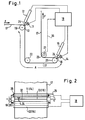
- a material web 17 possibly having holes at different points is continuously advanced in the direction of arrows F, F '.
- the web 17 is first guided around a deflection roller 19 by approximately 90 °, then runs down to a further deflection roller 22 which deflects the web 17 again by 90 ° in the opposite direction.
- the web 17 finally arrives at a deflection roller 20, around which the web 17 is guided through 180 °.
- the web then arrives at a further deflection roller 23 which deflects the web through 90 ° in a vertical direction, from where it is led upwards in the direction of arrow F 'from the arrangement.
- a laser scanner 12 and a photoelectric light receiving arrangement 11 are arranged on the deflecting roller 19.
- the laser scanner 12 generates a scanning light spot on the web resting on the deflecting roller 19, which spot periodically along a scanning line 13 in a Scans direction from edge to edge, which runs parallel to the axis of the deflection roller 19.
- the beam 24 emerging from the laser scanner 12 and displaced parallel to itself in a plane perpendicular to the plane of the drawing strikes the path 17 at a slightly different angle from the vertical, but relatively steeply in the region of the scanning line 13, so that the light receiving arrangement 11 is to be arranged at the angle of reflection to the surface of the web 17 in order to receive as much of the light reflected on the surface of the roller 19 as there is a hole 32 (FIGS. 2, 3).
- a second laser scanning device 15 of the same design is arranged above the deflection roller 20.
- a second photoelectric light receiving arrangement 14 which is designed and attached in a manner corresponding to the light receiving arrangement 11.
- the laser scanning devices 12, 15 and the light receiving arrangements 11, 14 are applied to evaluation electronics 18, which are also supplied with a feed clock signal by a feed sensor 21, so that the evaluation electronics 18 is informed about the degree of feed of the web 37 at all times.
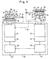
- the light receiving arrangements are designed as light guide rods 11 and 14, on one end of which a photomultiplier 25 is arranged, while the other end is provided with a mirror coating 26.
- a laser 27 optionally applies a mirror via optical means, not shown wheel 28, which deflects a reflected scanning light beam 29 to a plane mirror 30 in strip form, from which the scanning light beam is reflected back to a strip-shaped concave mirror 31, in the focal point of which the reflecting surfaces of the mirror wheel 28 are located.
- the travel beam 24, which is shifted parallel to itself, is generated, which emerges through a slot at the lower end of the housing 31 of the laser scanning device 12 or 15 and acts there on the surface of the web 17, so that the scanning along the line 13 there a laser light spot occurs.
- a hole in the track is shown at 32 in FIG. 3, for example. While the laser scanner 12 acts on the web 17 from above, the laser scanner 15 is arranged under the web 17, namely at a distance A (FIG. 1) from the laser scanner 12.
- the light guide rods 11 and 14 are shown separately in Fig. 3 only for the purpose of better detection compared to the laser scanning devices 12, 15. In fact, as in FIGS. 1 and 2, they are arranged under the reflection angle above and below the web 17.
- the distance A between the two scanning lines 13, 16 is illustrated in FIG. 1 by a line provided with arrows at the end; after installation of the device, it must be measured very precisely and stored in the evaluation electronics 18 so that the correct correlation is ensured.
- FIG. 3 shows the path on the right on the laser scanner 15 at a later point in time than on the laser scanner 12. Between the two positions shown in FIG. 3, the path 17 has traveled the distance A (FIG. 1) from the scanning line 13 to the scanning line 16.
- the evaluation electronics 18 following each light receiving arrangement 11 and 14 has a signal processing stage 33, 34 which, in addition to a signal for the current position of the mirror wheel 28 and the received signal from the photomultipliers 25, also in accordance with the dashed line Line 35 a signal representative of the feed of the web 37 is supplied.
- a threshold evaluation of the received signals and error detection take place in the signal processing stages 33.
- interfaces 36, 37 to two connected computers 38, 39 are provided, between which there is a computer interface, e.g. B. is a parallel interface.
- Suitable output devices such as printers or monitors are connected to the outputs 40, 41 of the computer 38, 39.
- the error information obtained and stored by the individual scans of the two laser scanning devices 12, 15 is correlated to total errors.
- the fault information is examined for possible holes, and the type of fault and minimum hole size are also determined.
- the holes can be output with longitudinal and transverse coordinates.
- the holes found are output via the outputs 40, 41 to suitable output devices as corresponding signals.
- the length assignment in the evaluation electronics 18 is carried out in that the individual scans of the laser scanning devices 12, 15 are synchronized in hardware with the path speed be set in order to be able to make an exact length specification (feed cycle adjustment).
- a feed clock is possible, or a signal representative of the feed is derived from the path, as is indicated by the dashed lines 35 in FIGS. 1 and 3. It is important that the inspection systems for the top and bottom are connected to the same feed clock. This means that the same cycle is always available dynamically.
- a window can be defined as a variable input parameter for the method in order to define a search area.
- the cross assignment is done in such a way that both laser scanners start scanning at the same web edge. For this purpose, both mechanical and electronic synchronization of the two mirror wheels 28 can take place.
- the counting of the transverse coordinate begins at the web edge via a hardware automatic edge. The cross assignment can therefore be carried out directly.
- a window can also be defined as a variable input parameter for the transverse coordinate in order to define a search area.
- a width threshold and an amplitude threshold can be set in the evaluation electronics 18 for the error detection during the scanning.
- the minimum hole size is a selectable parameter that can be used to define a certain minimum hole size.
- the minimum hole size to be found depends on the size of the laser light spot generated by the driving beam 24 on the scanning line 13 or 16 and on the belt speed and the scanning frequency.
- the minimum hole size that can be recognized is approximately 1.5 times the size of the light spot.
Landscapes
- Engineering & Computer Science (AREA)
- Textile Engineering (AREA)
- Physics & Mathematics (AREA)
- Health & Medical Sciences (AREA)
- Life Sciences & Earth Sciences (AREA)
- Chemical & Material Sciences (AREA)
- Analytical Chemistry (AREA)
- Biochemistry (AREA)
- General Health & Medical Sciences (AREA)
- General Physics & Mathematics (AREA)
- Immunology (AREA)
- Pathology (AREA)
- Length Measuring Devices By Optical Means (AREA)
- Investigating Materials By The Use Of Optical Means Adapted For Particular Applications (AREA)
Applications Claiming Priority (2)
| Application Number | Priority Date | Filing Date | Title |
|---|---|---|---|
| DE3739436A DE3739436C1 (de) | 1987-11-20 | 1987-11-20 | Optisches Lochsuchgeraet |
| DE3739436 | 1987-11-20 |
Publications (3)
| Publication Number | Publication Date |
|---|---|
| EP0316746A2 true EP0316746A2 (fr) | 1989-05-24 |
| EP0316746A3 EP0316746A3 (en) | 1990-06-06 |
| EP0316746B1 EP0316746B1 (fr) | 1993-08-04 |
Family
ID=6340933
Family Applications (1)
| Application Number | Title | Priority Date | Filing Date |
|---|---|---|---|
| EP88118660A Expired - Lifetime EP0316746B1 (fr) | 1987-11-20 | 1988-11-09 | Appareil de recherche de trous par voie optique |
Country Status (6)
| Country | Link |
|---|---|
| US (1) | US5095214A (fr) |
| EP (1) | EP0316746B1 (fr) |
| JP (1) | JPH01162138A (fr) |
| KR (1) | KR920003534B1 (fr) |
| AU (1) | AU607280B2 (fr) |
| DE (2) | DE3739436C1 (fr) |
Cited By (4)
| Publication number | Priority date | Publication date | Assignee | Title |
|---|---|---|---|---|
| EP0475454A3 (en) * | 1990-09-14 | 1992-10-14 | Fuji Photo Film Co., Ltd. | Defect inspection system |
| EP0668499A2 (fr) * | 1994-02-16 | 1995-08-23 | Cmd Corporation | Procédé et dispositif pour contrôler la formation d'une bande de matière |
| US5861078A (en) * | 1993-08-12 | 1999-01-19 | Cmd Corporation | Method and apparatus for detecting a seal on a plastic bag |
| EP0936459A1 (fr) * | 1998-02-13 | 1999-08-18 | Bähr GmbH Bremen - Industrie Technik | Procédé et appareil pour l'inspection du collage des couches dans une bande de feuille multicouche |
Families Citing this family (20)
| Publication number | Priority date | Publication date | Assignee | Title |
|---|---|---|---|---|
| US5383135A (en) * | 1992-12-31 | 1995-01-17 | Zellweger Uster, Inc. | Acquisition, measurement and control of thin webs on in-process textile materials |
| DE19506456C2 (de) * | 1995-02-24 | 1999-07-01 | Boewe Systec Ag | Kontrolleinrichtung zur Überwachung des Laufes zweier übereinanderliegender Papierbahnen in einer Papierverarbeitungsmaschine |
| US5644141A (en) * | 1995-10-12 | 1997-07-01 | The United States Of America As Represented By The Administrator Of The National Aeronautics And Space Administration | Apparatus and method for high-speed characterization of surfaces |
| US5994712A (en) * | 1997-07-29 | 1999-11-30 | Mack; John Edward | Belt flaw detector |
| US6895811B2 (en) * | 2001-12-14 | 2005-05-24 | Shawmut Corporation | Detection of small holes in laminates |
| DE20120977U1 (de) * | 2001-12-27 | 2003-04-30 | British American Tobacco (Germany) GmbH, 20354 Hamburg | Schnittkontrolle für eine Innenumhüllung für eine Zigarettengruppe |
| DE10204939A1 (de) * | 2002-02-07 | 2003-09-04 | Parsytec Comp Gmbh | Vorrichtung und Verfahren zur Erzeugung von flächigem parallelen Licht |
| US8210791B2 (en) * | 2004-05-03 | 2012-07-03 | Jervis B. Webb Company | Automatic transport loading system and method |
| US7980808B2 (en) * | 2004-05-03 | 2011-07-19 | Jervis B. Webb Company | Automatic transport loading system and method |
| US8075243B2 (en) | 2004-05-03 | 2011-12-13 | Jervis B. Webb Company | Automatic transport loading system and method |
| WO2005108246A2 (fr) * | 2004-05-03 | 2005-11-17 | Jervis B. Webb Company | Systeme de chargement de transport automatique et procédé |
| US8192137B2 (en) | 2004-05-03 | 2012-06-05 | Jervis B. Webb Company | Automatic transport loading system and method |
| JP4456426B2 (ja) * | 2004-07-06 | 2010-04-28 | 富士フイルム株式会社 | 検出装置 |
| US20060276958A1 (en) * | 2005-06-02 | 2006-12-07 | Jervis B. Webb Company | Inertial navigational guidance system for a driverless vehicle utilizing laser obstacle sensors |
| WO2010039135A1 (fr) * | 2008-10-01 | 2010-04-08 | Hewlett-Packard Development Company, L.P. | Support de bande pour caméra |
| DE202013102069U1 (de) * | 2013-05-13 | 2014-08-14 | Eltromat Gmbh | Farbmesseinrichtung, insbesondere für Druckmaschinen |
| KR101567708B1 (ko) | 2014-07-09 | 2015-11-10 | 현대자동차주식회사 | 연료전지 막-전극 접합체의 결함 검출 방법 및 장치 |
| KR101741224B1 (ko) * | 2015-05-08 | 2017-05-30 | 주식회사 한성시스코 | 타이어 보강벨트의 텍스타일 코드 개수 검사장치 |
| CN104949992A (zh) * | 2015-05-19 | 2015-09-30 | 东莞市威力固电路板设备有限公司 | 印刷电路板自动光学检测系统及其印刷电路板载物台 |
| CN108788893B (zh) * | 2018-07-20 | 2023-12-05 | 中铁武汉电气化局集团第一工程有限公司 | 一种平腕臂安装孔寻孔装置 |
Citations (5)
| Publication number | Priority date | Publication date | Assignee | Title |
|---|---|---|---|---|
| US3786265A (en) * | 1973-02-02 | 1974-01-15 | Lindly Company Inc | Apparatus for detecting defects in continuous traveling material |
| US4310250A (en) * | 1980-02-01 | 1982-01-12 | Erwin Sick Gmbh | Apparatus for monitoring for faults in translucent strip material |
| JPS61175552A (ja) * | 1985-01-30 | 1986-08-07 | Kanzaki Paper Mfg Co Ltd | 欠陥シ−トの検出方法 |
| DE3544871A1 (de) * | 1984-12-19 | 1986-09-11 | Erwin Sick Gmbh Optik-Elektronik, 7808 Waldkirch | Optisches fehlersuchgeraet |
| JPS61217747A (ja) * | 1985-03-23 | 1986-09-27 | Yodogawa Seikosho:Kk | ピンホ−ル検出装置 |
Family Cites Families (18)
| Publication number | Priority date | Publication date | Assignee | Title |
|---|---|---|---|---|
| NL202843A (fr) * | 1954-12-16 | |||
| DE1235034B (de) * | 1959-02-26 | 1967-02-23 | Licentia Gmbh | Elektrische Auswerteschaltung fuer eine Oberflaechen-Abtastvorrichtung |
| DE1297892B (de) * | 1963-04-23 | 1969-06-19 | Lippke Paul | Einrichtung zur elektro-optischen Pruefung von bewegten Bahnen oder Bogen |
| CH543088A (de) * | 1970-09-23 | 1973-10-15 | Ciba Geigy Ag | Vorrichtung zur kontinuierlichen Überprüfung eines photographischen Filmes auf Rissstellen |
| FR2126370B1 (fr) * | 1971-02-24 | 1973-06-29 | Columbia Research Corp | |
| DE2808359C3 (de) * | 1978-02-27 | 1980-09-04 | Erwin Sick Gmbh Optik-Elektronik, 7808 Waldkirch | Suchgerät für Löcher in Bahnen |
| DE2827705C3 (de) * | 1978-06-23 | 1981-07-30 | Erwin Sick Gmbh Optik-Elektronik, 7808 Waldkirch | Gerät zur Feststellung von Fehlern an Bahnmaterial |
| DE2904433C2 (de) * | 1979-02-06 | 1984-05-17 | Erwin Sick Gmbh Optik-Elektronik, 7808 Waldkirch | Filmfehler-Überwachungsgerät |
| DE2934554C2 (de) * | 1979-08-27 | 1984-08-02 | Erwin Sick Gmbh Optik-Elektronik, 7808 Waldkirch | Optoelektronisches Überwachungsgerät. |
| DE2947791C2 (de) * | 1979-11-28 | 1985-04-18 | Licentia Patent-Verwaltungs-Gmbh, 6000 Frankfurt | Einrichtung zur Farbüberwachung von bogen- oder bahnförmigen, in Bewegung befindlichen Materialien, insbesondere der Druckmaterialien von Druckmaschinen |
| DE3013549C2 (de) * | 1980-04-09 | 1984-06-14 | Erwin Sick Gmbh Optik-Elektronik, 7808 Waldkirch | Anordnung zur Signalauswertung bei einem Lochsuchgerät |
| US4389575A (en) * | 1980-07-03 | 1983-06-21 | Sparton Corporation | Fabric inspection system |
| GB2081891A (en) * | 1980-08-11 | 1982-02-24 | Wiggins Teape The Group Ltd | Web monitoring apparatus |
| JPS6333160Y2 (fr) * | 1980-09-27 | 1988-09-05 | ||
| CH656466A5 (de) * | 1982-02-15 | 1986-06-30 | Alusuisse | Verfahren und vorrichtung zur oberflaechenkontrolle eines werkstoffes. |
| KR890002004B1 (ko) * | 1984-01-11 | 1989-06-07 | 가부시끼 가이샤 도오시바 | 지폐류 판별장치 |
| GB8501910D0 (en) * | 1985-01-25 | 1985-02-27 | Haigh Chadwick Ltd | Web monitoring arrangement |
| US4728800A (en) * | 1985-04-24 | 1988-03-01 | Young Engineering, Inc. | Apparatus and method for detecting defects in a moving web |
-
1987
- 1987-11-20 DE DE3739436A patent/DE3739436C1/de not_active Expired
-
1988
- 1988-11-09 EP EP88118660A patent/EP0316746B1/fr not_active Expired - Lifetime
- 1988-11-09 DE DE8888118660T patent/DE3882915D1/de not_active Expired - Fee Related
- 1988-11-15 AU AU25142/88A patent/AU607280B2/en not_active Ceased
- 1988-11-16 US US07/272,195 patent/US5095214A/en not_active Expired - Fee Related
- 1988-11-19 KR KR1019880015245A patent/KR920003534B1/ko not_active IP Right Cessation
- 1988-11-21 JP JP63294476A patent/JPH01162138A/ja active Pending
Patent Citations (5)
| Publication number | Priority date | Publication date | Assignee | Title |
|---|---|---|---|---|
| US3786265A (en) * | 1973-02-02 | 1974-01-15 | Lindly Company Inc | Apparatus for detecting defects in continuous traveling material |
| US4310250A (en) * | 1980-02-01 | 1982-01-12 | Erwin Sick Gmbh | Apparatus for monitoring for faults in translucent strip material |
| DE3544871A1 (de) * | 1984-12-19 | 1986-09-11 | Erwin Sick Gmbh Optik-Elektronik, 7808 Waldkirch | Optisches fehlersuchgeraet |
| JPS61175552A (ja) * | 1985-01-30 | 1986-08-07 | Kanzaki Paper Mfg Co Ltd | 欠陥シ−トの検出方法 |
| JPS61217747A (ja) * | 1985-03-23 | 1986-09-27 | Yodogawa Seikosho:Kk | ピンホ−ル検出装置 |
Non-Patent Citations (2)
| Title |
|---|
| PATENT ABSTRACTS OF JAPAN, Band 10, Nr. 387 (P-530)[2444], 25. Dezember 1986; & JP-A-61 175 552 (KANZAKI) 07-08-1986 * |
| PATENT ABSTRACTS OF JAPAN, Band 11, Nr. 49 (P-547)[2496], 14. Februar 1987; & JP-A-61 217 747 (YODOGAWA SEIKOSHO) 27-09-1986 * |
Cited By (6)
| Publication number | Priority date | Publication date | Assignee | Title |
|---|---|---|---|---|
| EP0475454A3 (en) * | 1990-09-14 | 1992-10-14 | Fuji Photo Film Co., Ltd. | Defect inspection system |
| US5861078A (en) * | 1993-08-12 | 1999-01-19 | Cmd Corporation | Method and apparatus for detecting a seal on a plastic bag |
| EP0668499A2 (fr) * | 1994-02-16 | 1995-08-23 | Cmd Corporation | Procédé et dispositif pour contrôler la formation d'une bande de matière |
| EP0668499A3 (fr) * | 1994-02-16 | 1997-01-02 | Cmd Corp | Procédé et dispositif pour contrÔler la formation d'une bande de matière. |
| EP0936459A1 (fr) * | 1998-02-13 | 1999-08-18 | Bähr GmbH Bremen - Industrie Technik | Procédé et appareil pour l'inspection du collage des couches dans une bande de feuille multicouche |
| DE19805932A1 (de) * | 1998-02-13 | 1999-08-19 | Baehr Gmbh Bremen Ind Technik | Verfahren und Vorrichtung zum Prüfen der Verklebung von Folienlagen mehrlagiger Folienbahnen |
Also Published As
| Publication number | Publication date |
|---|---|
| US5095214A (en) | 1992-03-10 |
| DE3882915D1 (de) | 1993-09-09 |
| KR920003534B1 (ko) | 1992-05-02 |
| DE3739436C1 (de) | 1989-03-30 |
| AU607280B2 (en) | 1991-02-28 |
| JPH01162138A (ja) | 1989-06-26 |
| AU2514288A (en) | 1989-05-25 |
| EP0316746B1 (fr) | 1993-08-04 |
| EP0316746A3 (en) | 1990-06-06 |
| KR890008562A (ko) | 1989-07-12 |
Similar Documents
| Publication | Publication Date | Title |
|---|---|---|
| EP0316746B1 (fr) | Appareil de recherche de trous par voie optique | |
| DE2808359C3 (de) | Suchgerät für Löcher in Bahnen | |
| DE2433683C3 (de) | Vorrichtung zur Überwachung einer Materialbahn auf Fehlstellen | |
| EP0123929B1 (fr) | Dispositif pour la détection de défauts | |
| EP0650911B1 (fr) | Dispositif et procédé pour reconnaítre le chevauchement d'envois plats flexibles | |
| DE10017862A1 (de) | Optoelektronische Vorrichtung | |
| DE2338295C2 (de) | Vorrichtung zum Feststellen von Fehlern auf gegenüberliegenden Flächen einer im wesentlichen ebenen Bahn | |
| EP0281747A2 (fr) | Rideau de lumière | |
| DE3602008C2 (fr) | ||
| DE69203259T2 (de) | Apparat zum Abtasten von Gegenständen in Blattform. | |
| DE2808360C3 (de) | Optische Vorrichtung zur Bestimmung des Lichtaustrittswinkels | |
| DE2653298A1 (de) | Pruefvorrichtung zum pruefen der enden von zigaretten | |
| DE19914962C2 (de) | Optoelektronische Vorrichtung | |
| DE2827705C3 (de) | Gerät zur Feststellung von Fehlern an Bahnmaterial | |
| DE3411934C2 (de) | Fehlerfeststellungsvorrichtung | |
| DE102020104931B4 (de) | Verfahren und Vorrichtung zur Kantenerkennung eines Objekts | |
| EP0009581A1 (fr) | Procédé pour déterminer l'épaisseur de bandes qui passent sur des rouleaux | |
| DE2340688C3 (de) | Lesevorrichtung für optisch erfaßbare digitale Codierungen | |
| DE2718086C2 (de) | Vorrichtung zur Feststellung von Oberflächenfehlern von Stahlteilen | |
| EP1021293A1 (fr) | Dispositif permettant de produire des decoupes destinees a des emballages | |
| DE10101443B4 (de) | Verfahren zur Ermittlung eines Schnittbildes einer Objektstruktur | |
| DE1524368A1 (de) | Lochstreifenleser | |
| DE29811486U1 (de) | Optoelektronischer Sensor | |
| DE3408106A1 (de) | Optischer rauheits-scanner | |
| EP0049419A1 (fr) | Procédé pour la correction d'un signal de mesure |
Legal Events
| Date | Code | Title | Description |
|---|---|---|---|
| PUAI | Public reference made under article 153(3) epc to a published international application that has entered the european phase |
Free format text: ORIGINAL CODE: 0009012 |
|
| 17P | Request for examination filed |
Effective date: 19881109 |
|
| AK | Designated contracting states |
Kind code of ref document: A2 Designated state(s): BE DE FR GB IT SE |
|
| PUAL | Search report despatched |
Free format text: ORIGINAL CODE: 0009013 |
|
| AK | Designated contracting states |
Kind code of ref document: A3 Designated state(s): BE DE FR GB IT SE |
|
| 17Q | First examination report despatched |
Effective date: 19920313 |
|
| GRAA | (expected) grant |
Free format text: ORIGINAL CODE: 0009210 |
|
| AK | Designated contracting states |
Kind code of ref document: B1 Designated state(s): BE DE FR GB IT SE |
|
| PG25 | Lapsed in a contracting state [announced via postgrant information from national office to epo] |
Ref country code: SE Effective date: 19930804 Ref country code: BE Effective date: 19930804 |
|
| ITF | It: translation for a ep patent filed | ||
| GBT | Gb: translation of ep patent filed (gb section 77(6)(a)/1977) |
Effective date: 19930809 |
|
| REF | Corresponds to: |
Ref document number: 3882915 Country of ref document: DE Date of ref document: 19930909 |
|
| ET | Fr: translation filed | ||
| PGFP | Annual fee paid to national office [announced via postgrant information from national office to epo] |
Ref country code: GB Payment date: 19931025 Year of fee payment: 6 |
|
| PGFP | Annual fee paid to national office [announced via postgrant information from national office to epo] |
Ref country code: FR Payment date: 19931116 Year of fee payment: 6 |
|
| PGFP | Annual fee paid to national office [announced via postgrant information from national office to epo] |
Ref country code: DE Payment date: 19931223 Year of fee payment: 6 |
|
| PLBE | No opposition filed within time limit |
Free format text: ORIGINAL CODE: 0009261 |
|
| STAA | Information on the status of an ep patent application or granted ep patent |
Free format text: STATUS: NO OPPOSITION FILED WITHIN TIME LIMIT |
|
| 26N | No opposition filed | ||
| PG25 | Lapsed in a contracting state [announced via postgrant information from national office to epo] |
Ref country code: GB Effective date: 19941109 |
|
| GBPC | Gb: european patent ceased through non-payment of renewal fee |
Effective date: 19941109 |
|
| PG25 | Lapsed in a contracting state [announced via postgrant information from national office to epo] |
Ref country code: FR Effective date: 19950731 |
|
| PG25 | Lapsed in a contracting state [announced via postgrant information from national office to epo] |
Ref country code: DE Effective date: 19950801 |
|
| REG | Reference to a national code |
Ref country code: FR Ref legal event code: ST |
|
| PG25 | Lapsed in a contracting state [announced via postgrant information from national office to epo] |
Ref country code: IT Free format text: LAPSE BECAUSE OF NON-PAYMENT OF DUE FEES;WARNING: LAPSES OF ITALIAN PATENTS WITH EFFECTIVE DATE BEFORE 2007 MAY HAVE OCCURRED AT ANY TIME BEFORE 2007. THE CORRECT EFFECTIVE DATE MAY BE DIFFERENT FROM THE ONE RECORDED. Effective date: 20051109 |