EP0314221A2 - Halbleiterschalter mit parallelen lateralen DMOS und IGT - Google Patents
Halbleiterschalter mit parallelen lateralen DMOS und IGT Download PDFInfo
- Publication number
- EP0314221A2 EP0314221A2 EP88202237A EP88202237A EP0314221A2 EP 0314221 A2 EP0314221 A2 EP 0314221A2 EP 88202237 A EP88202237 A EP 88202237A EP 88202237 A EP88202237 A EP 88202237A EP 0314221 A2 EP0314221 A2 EP 0314221A2
- Authority
- EP
- European Patent Office
- Prior art keywords
- region
- conductivity type
- major surface
- channel region
- adjoining
- Prior art date
- Legal status (The legal status is an assumption and is not a legal conclusion. Google has not performed a legal analysis and makes no representation as to the accuracy of the status listed.)
- Granted
Links
Images
Classifications
-
- H—ELECTRICITY
- H10—SEMICONDUCTOR DEVICES; ELECTRIC SOLID-STATE DEVICES NOT OTHERWISE PROVIDED FOR
- H10D—INORGANIC ELECTRIC SEMICONDUCTOR DEVICES
- H10D12/00—Bipolar devices controlled by the field effect, e.g. insulated-gate bipolar transistors [IGBT]
- H10D12/411—Insulated-gate bipolar transistors [IGBT]
-
- H—ELECTRICITY
- H03—ELECTRONIC CIRCUITRY
- H03K—PULSE TECHNIQUE
- H03K17/00—Electronic switching or gating, i.e. not by contact-making and –breaking
- H03K17/08—Modifications for protecting switching circuit against overcurrent or overvoltage
- H03K17/082—Modifications for protecting switching circuit against overcurrent or overvoltage by feedback from the output to the control circuit
- H03K17/0822—Modifications for protecting switching circuit against overcurrent or overvoltage by feedback from the output to the control circuit in field-effect transistor switches
-
- H—ELECTRICITY
- H02—GENERATION; CONVERSION OR DISTRIBUTION OF ELECTRIC POWER
- H02M—APPARATUS FOR CONVERSION BETWEEN AC AND AC, BETWEEN AC AND DC, OR BETWEEN DC AND DC, AND FOR USE WITH MAINS OR SIMILAR POWER SUPPLY SYSTEMS; CONVERSION OF DC OR AC INPUT POWER INTO SURGE OUTPUT POWER; CONTROL OR REGULATION THEREOF
- H02M3/00—Conversion of DC power input into DC power output
- H02M3/02—Conversion of DC power input into DC power output without intermediate conversion into AC
- H02M3/04—Conversion of DC power input into DC power output without intermediate conversion into AC by static converters
- H02M3/10—Conversion of DC power input into DC power output without intermediate conversion into AC by static converters using discharge tubes with control electrode or semiconductor devices with control electrode
- H02M3/145—Conversion of DC power input into DC power output without intermediate conversion into AC by static converters using discharge tubes with control electrode or semiconductor devices with control electrode using devices of a triode or transistor type requiring continuous application of a control signal
- H02M3/155—Conversion of DC power input into DC power output without intermediate conversion into AC by static converters using discharge tubes with control electrode or semiconductor devices with control electrode using devices of a triode or transistor type requiring continuous application of a control signal using semiconductor devices only
- H02M3/156—Conversion of DC power input into DC power output without intermediate conversion into AC by static converters using discharge tubes with control electrode or semiconductor devices with control electrode using devices of a triode or transistor type requiring continuous application of a control signal using semiconductor devices only with automatic control of output voltage or current, e.g. switching regulators
- H02M3/158—Conversion of DC power input into DC power output without intermediate conversion into AC by static converters using discharge tubes with control electrode or semiconductor devices with control electrode using devices of a triode or transistor type requiring continuous application of a control signal using semiconductor devices only with automatic control of output voltage or current, e.g. switching regulators including plural semiconductor devices as final control devices for a single load
- H02M3/1584—Conversion of DC power input into DC power output without intermediate conversion into AC by static converters using discharge tubes with control electrode or semiconductor devices with control electrode using devices of a triode or transistor type requiring continuous application of a control signal using semiconductor devices only with automatic control of output voltage or current, e.g. switching regulators including plural semiconductor devices as final control devices for a single load with a plurality of power processing stages connected in parallel
-
- H—ELECTRICITY
- H03—ELECTRONIC CIRCUITRY
- H03K—PULSE TECHNIQUE
- H03K17/00—Electronic switching or gating, i.e. not by contact-making and –breaking
- H03K17/51—Electronic switching or gating, i.e. not by contact-making and –breaking characterised by the components used
- H03K17/56—Electronic switching or gating, i.e. not by contact-making and –breaking characterised by the components used by the use, as active elements, of semiconductor devices
- H03K17/567—Circuits characterised by the use of more than one type of semiconductor device, e.g. BIMOS, composite devices such as IGBT
-
- H—ELECTRICITY
- H10—SEMICONDUCTOR DEVICES; ELECTRIC SOLID-STATE DEVICES NOT OTHERWISE PROVIDED FOR
- H10D—INORGANIC ELECTRIC SEMICONDUCTOR DEVICES
- H10D30/00—Field-effect transistors [FET]
- H10D30/60—Insulated-gate field-effect transistors [IGFET]
- H10D30/64—Double-diffused metal-oxide semiconductor [DMOS] FETs
- H10D30/65—Lateral DMOS [LDMOS] FETs
-
- H—ELECTRICITY
- H10—SEMICONDUCTOR DEVICES; ELECTRIC SOLID-STATE DEVICES NOT OTHERWISE PROVIDED FOR
- H10D—INORGANIC ELECTRIC SEMICONDUCTOR DEVICES
- H10D84/00—Integrated devices formed in or on semiconductor substrates that comprise only semiconducting layers, e.g. on Si wafers or on GaAs-on-Si wafers
- H10D84/80—Integrated devices formed in or on semiconductor substrates that comprise only semiconducting layers, e.g. on Si wafers or on GaAs-on-Si wafers characterised by the integration of at least one component covered by groups H10D12/00 or H10D30/00, e.g. integration of IGFETs
- H10D84/82—Integrated devices formed in or on semiconductor substrates that comprise only semiconducting layers, e.g. on Si wafers or on GaAs-on-Si wafers characterised by the integration of at least one component covered by groups H10D12/00 or H10D30/00, e.g. integration of IGFETs of only field-effect components
- H10D84/83—Integrated devices formed in or on semiconductor substrates that comprise only semiconducting layers, e.g. on Si wafers or on GaAs-on-Si wafers characterised by the integration of at least one component covered by groups H10D12/00 or H10D30/00, e.g. integration of IGFETs of only field-effect components of only insulated-gate FETs [IGFET]
-
- H—ELECTRICITY
- H03—ELECTRONIC CIRCUITRY
- H03K—PULSE TECHNIQUE
- H03K2217/00—Indexing scheme related to electronic switching or gating, i.e. not by contact-making or -breaking covered by H03K17/00
- H03K2217/0036—Means reducing energy consumption
Definitions
- the invention relates to a semiconductor switch including a lateral insulated gate transistor (LIGT) which is transferable between a conducting state and a nonconducting state and which has a second gate, a cathode region and an anode region and semiconductor device comprising such a switch. More particularly it is an invention involving a semiconductor switch for power switching which can be readily fabricated in a monolithic integrated circuit.
- LIGT lateral insulated gate transistor
- Various types of power switching semiconductor devices are known. Included among these are hybrid devices in which two different device structures are fabricated on a single semiconductor chip.
- One such hybrid device which has been proposed in the past combines a power MOS transistor with a vertical insulated gate transistor. This combination is acceptable in a separate device but cannot be fabricated in a monolithic integrated circuit together with numerous other devices because the vertical insulated gate transistor uses the substrate as one of its contacts.
- a semiconductor switch characterized in that the switch includes a lateral double diffused MOS transistor which is transferable between a conducting state and a nonconducting state and which has a first gate, a source region and a drain region, said source region and said cathode region being interconnected, said drain region and said anode region being interconnected, signal means connected to said second gate and capable of transmitting signals thereto for causing said lateral insulated gate transistor to transfer between its current conducting state and its nonconducting state, delay means connected to said first gate and capable of transmitting signals thereto to cause said double diffused MOS transistor to transfer between its current conducting state and its nonconducting state, and means for producing a reference signal representative of the current through said lateral insulated gate transistor, said delay means being responsive to a signal from said signal means for causing said lateral insulated gate transistor to transfer to its nonconducting state and to a signal representative of the current through said lateral insulated gate transistor to generate a signal to transfer said double diffused MOS transistor
- One of the features of the invention is the use of a lateral insulated gate transistor in a parallel circuit with a lateral DMOS transistor for primarily inductive switching operations. This provides one of the advantages of the invention. By using a lateral insulated gate transistor, its area efficiency is obtained and by connecting it in parallel with a relatively small lateral DMOS for turnoff operation a fast switch is obtained which takes up less than one-fifth the silicon area which a DMOS of comparable capacity would occupy.
- Another advantage of the invention is the low power dissipation during turn off compared to a lateral insulated gate transistor alone.
- a semiconductor device comprising a semiconductor substrate of a first conductivity type having a major surface.
- An epitaxial layer of a second conductivity type opposite to that of the first conductivity type is on the substrate forming part of the major surface.
- a major surface adjoining first channel region of the first conductivity type is in the epitaxial layer.
- a major surface adjoining drain region of the second conductivity type is also in the epitaxial layer spaced from the first channel region.
- a major surface adjoining source region of the second conductivity type is located in the first channel region.
- the first channel region together with the source region and the drain region form a lateral double diffused MOS transistor.
- the device also includes a major surface adjoining anode region of the first conductivity type in the epitaxial layer adjacent the drain region.
- a major surface-adjoining second channel region of the first conductivity type is also in the epitaxial layer spaced from the anode region.
- a major surface-adjoining cathode region of the second conductivity type is located in the second channel region.
- the anode region, the cathode region and the second channel region form a lateral insulated gate transistor.
- a semiconductor device having a major surface comprising a semiconductor substrate of a first conductivity type.
- An epitaxial layer of a second conductivity type opposite to that of the first conductivity type is on the substrate forming part of the major surface.
- a major surface adjoining source region of the second conductivity type is also included.
- a major surface adjoining drain region of said second conductivity type is in the epitaxial layer.
- a major surface adjoining first channel region of the first conductivity type is located between the source region and the drain region. The first channel region together with the source region and the drain region form a lateral double diffused MOS transistor.
- a major surface adjoining cathode region of the second conductivity type is also included.
- a major surface-adjoining anode region of the first conductivity type is in the epitaxial layer.
- a major surface-adjoining second channel region of the first conductivity type is located between the anode and the cathode regions.
- the anode and cathode regions and the second channel region form a lateral insulated gate transitor.
- the source region is in the first channel region.
- the cathode region is in the second channel region.
- the second channel region extends down to the substrate for isolating purposes except in a small section of the device where the epitaxial region isolates the second channel region from the substrate.
- the second channel region in the small section isolates the cathode region in the small section from the cathode region in the rest of the device.
- the channel region in the small section is separated from the channel region in the rest of the device by the epitaxial region.
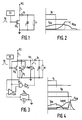
- FIG. 1 there is shown a lateral insulated gate transistor Qig.
- transistor Qig In circuit with transistor Qig is an inductance L, rectifier D1, capacitance C and a load represented by resistor R. Such a circuit is intended to be representative of the input of a ballast lighting circuit. Voltage V cc is the operating voltage for the circuit.
- a signal source SS is connected to the gate of transistor Qig to apply a gate signal V G thereto.
- the circuitry of Figure 3 is disclosed herein.
- the same inductive circuit as in Figure 1 with its inductance L, capacitance C, rectifier D1, and load represented by resistor R is controlled by lateral insulated gate transistor Qig.
- a lateral double diffused MOS transistor OMOS is connected in parallel with the conducting path of transistor Qig.
- the anode region of transistor Qig is connected to the drain region of transistor QMOS.
- the cathode region of transistor Qig is connected to ground to which the source region of transistor QMOS is also connected.
- current source I with resistor R1 connected in parallel forming a reference signal source.
- the output of current source I is connected to one input of comparator COM.
- the other input of comparator COM is connected to a tap between resistor R2 and the series connected source of sensing transistor Qs.
- the gate of sensing transistor Qs is connected to the gate of transistor Qig and its drain is connected to the anode of transistor Qig.
- the gates of transistors Qig and Qs are also connected to signal source means SS.
- the source of sensing transistor Qs is connected to ground.
- the enable input of comparator COM is connected to the gate of transistor Qig.
- the output of comparator COM is connected to one input of "or” gate OR.
- the other input of the "or” gate is connected to the gate of transistor Qig.
- the output of "or” gate OR is connected to the input of buffer B whose output is connected to the gate of LDMOS transistor QMOS.
- comparator COM As long as a gate voltage V G is applied to the gate of lateral transistor Qig by signal source means SS, comparator COM is disabled. When the gate voltage V G is removed comparator COM is enabled. This comparator functions to compare the current through transistor Qs with that from the reference signal source. As will be explained, because of its structure, the current through transistor Qs is indicative of the current through transistor Qig. As long as the current through transistor Qs is larger than the reference provided by current source I, "or" gate OR produces an output because it has an input either from gate voltage V G or from comparator COM. As a consequence buffer B provides a gate voltage V G1 to the gate of transistor QMOS to maintain it in the on condition.
- Figure 3 shows a representative structure for transistors Qig and QMOS as they would appear in such a monolithic integrated circuit.
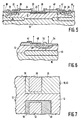
- Shown in Figure 5 is a semiconductor substrate 10 of a first conductivity type, typically p-type, with an epitaxial surface layer 12 of a second conductivity type opposite to that of the first, typically n-type.
- the expitaxial layer is provided on the top surface of substrate 10 and provides part of a major surface 14.
- a major surface adjoining first channel region 16 of a first conductivity type is provided in the epitaxial layer and forms a p-n junction therewith.
- a major surface adjoining source region 18 of the second conductivity type is provided in first channel region 16.
- a major surface adjoining drain region 20 also of the second conductivity type is provided in the epitaxial layer at a location which is spaced apart from first channel region 16.
- First channel region 16 has a surface adjoining portion 22 located between the source and drain regions of the device which forms a channel of a lateral DMOS transistor.
- An insulating layer 24 is provided on the epitaxial surface layer 12 and covers at least that portion of the first channel region 16 located between the source and drain regions of the transistor.
- a gate electrode 26 is provided on the insulating layer over channel 22. Source electrode 28 and drain electrode 30 provide electrical connections respectively to the source and drain regions of the transistor.
- Buried layer 34 extends beneath first channel region 16 and part of epitaxial layer 12 between source and drain regions 18 and 20. Buried layer 34 extends across the entire area below gate electrode 26 and stops shortly thereafter. First channel region 16 and buried layer 34 extend down to substrate 10 to provide isolation. If the foregoing were all that was fabricated in the monolithic integrated circuit one would have a well known DMOS transistor, similar to that disclosed in U.S. Patent 4.300.150.
- an additional surface adjoining second channel region 35 of the first conductivity type is provided in epitaxial layer 12.
- a further surface adjoining cathode region 36 of the second conductivity type is provided in second channel region 35. This forms the cathode region of a further to be described lateral insulated gate transistor.
- a surface adjoining anode region 38 of the first conductivity type is provided in the epitaxial layer at a location which is spaced apart from second channel region 35.
- Second channel region 35 has a surface adjoining portion 39 located between cathode region 36 and anode region 38 which forms a channel for the lateral insulated gate transistor.
- An insulating layer 40 is provided on the surface of epitaxial layer 12 and covers at least that portion of second channel region 35 located between anode and cathode regions 36 and 38 of this lateral insulated gate transistor.
- a gate electrode 42 is provided on insulating layer 40 over second channel 35.
- the anode 38 of the lateral insulated gate transistor is connected to the drain region 20 of the lateral DMOS transistor by having common electrode 30 provide electrical connections to both.
- Cathode electrode 44 contacts both cathode region 36 and second channel region 35 providing a conventional cathode short therebe tween.
- P-type buried region 45 is provided under channel region 35 and between the cathode and anode regions. As is shown buried layer 45 will typically extend across the entire area below the gate electrode and stop shortly thereafter. This buried layer provides field shaping for the lateral insulated gate transistor. Second channel region 35 and buried layer 45 extend down to substrate 10 to provide isolation.
- a monolithic integrated circuit of which the disclosed lateral DMOS transistor and lateral insulated gate transistor can form a part could also include the components shown in Figure 3 including resistors R, R1 and R2, capacitor C, comparator COM, diode D1, "or" circuit OR, buffer B and current source I. All of these would also be fabricated by standard techniques.
- Figures 6 and 7 show the manner in which transistor Qs is fabricated in the monolithic integrated circuit.
- a small section of the circuit is reserved for this purpose.
- Second channel region 48 and its surface adjoining portion 49 in the small section is separated from second channel region 35 and its surface adjoining portion 39 in the rest of the structure by n-type epitaxial region 12.
- Epitaxial region 12 also isolates second channel region 48 from p-type regions 45 and 10 in this small section.
- Gate contact 42 ( Figures 5 and 6), however, is common for both channel region 35 and channel region 48.
- cathode region 52 in this small section is separated from cathode region 36 in transistor Qig and is isolated by channel region 48.
- contact 54 ( Figure 6) is provided for cathode region 52 in this section.
- Contact 54 it is to be understood is separate from contact 44 ( Figure 5) which contacts cathode region 36 in that part of transistor Qig not comprising transistor Qs.
- resistor R2 can be connected between cathode contact 54 of transistor Qs and cathode contact 44 of transistor Qig as shown in Figure 3. Since transistor Qs is part of the same structure as transistor Qig it is to be understood that it conducts a current which is indicative of the current through transistor Qig.
Landscapes
- Engineering & Computer Science (AREA)
- Power Engineering (AREA)
- Insulated Gate Type Field-Effect Transistor (AREA)
- Metal-Oxide And Bipolar Metal-Oxide Semiconductor Integrated Circuits (AREA)
Applications Claiming Priority (2)
| Application Number | Priority Date | Filing Date | Title |
|---|---|---|---|
| US115478 | 1987-10-30 | ||
| US07/115,478 US4939566A (en) | 1987-10-30 | 1987-10-30 | Semiconductor switch with parallel DMOS and IGT |
Publications (3)
| Publication Number | Publication Date |
|---|---|
| EP0314221A2 true EP0314221A2 (de) | 1989-05-03 |
| EP0314221A3 EP0314221A3 (en) | 1990-08-08 |
| EP0314221B1 EP0314221B1 (de) | 1994-06-29 |
Family
ID=22361663
Family Applications (1)
| Application Number | Title | Priority Date | Filing Date |
|---|---|---|---|
| EP88202237A Expired - Lifetime EP0314221B1 (de) | 1987-10-30 | 1988-10-06 | Halbleiterschalter mit parallelen lateralen DMOS und IGT |
Country Status (6)
| Country | Link |
|---|---|
| US (1) | US4939566A (de) |
| EP (1) | EP0314221B1 (de) |
| JP (1) | JP2545123B2 (de) |
| KR (1) | KR0134093B1 (de) |
| DE (1) | DE3850473T2 (de) |
| HU (1) | HU212519B (de) |
Cited By (6)
| Publication number | Priority date | Publication date | Assignee | Title |
|---|---|---|---|---|
| DE4207187A1 (de) * | 1991-03-08 | 1992-09-10 | Fuji Electric Co Ltd | Halbleiter-schaltvorrichtung mit verringertem schaltverlust |
| EP0726654A1 (de) * | 1995-02-10 | 1996-08-14 | Siemens Aktiengesellschaft | Integrierbarer Umschalter für höhere Spannungen |
| DE19523096A1 (de) * | 1995-06-26 | 1997-01-02 | Abb Management Ag | Stromrichterschaltungsanordnung |
| WO2000005766A3 (en) * | 1998-07-24 | 2000-04-27 | Koninkl Philips Electronics Nv | Silicon-on-insulator (soi) hybrid transistor device structure |
| WO2001008298A1 (en) * | 1999-07-23 | 2001-02-01 | Nokia Corporation | Amplifier having bias circuit self-compensating for vgs process variation and ids aging |
| WO2006036963A2 (en) | 2004-09-28 | 2006-04-06 | Texas Instruments Incorporated | Current limiting circuit for high-speed low-side driver outputs |
Families Citing this family (24)
| Publication number | Priority date | Publication date | Assignee | Title |
|---|---|---|---|---|
| EP0371785B1 (de) * | 1988-11-29 | 1996-05-01 | Kabushiki Kaisha Toshiba | Lateraler Leitfähigkeitsmodulations-MOSFET |
| US5155562A (en) * | 1990-02-14 | 1992-10-13 | Fuji Electric Co., Ltd. | Semiconductor device equipped with a conductivity modulation misfet |
| US5072268A (en) * | 1991-03-12 | 1991-12-10 | Power Integrations, Inc. | MOS gated bipolar transistor |
| US5374843A (en) * | 1991-05-06 | 1994-12-20 | Silinconix, Inc. | Lightly-doped drain MOSFET with improved breakdown characteristics |
| US5386136A (en) * | 1991-05-06 | 1995-01-31 | Siliconix Incorporated | Lightly-doped drain MOSFET with improved breakdown characteristics |
| US6091164A (en) * | 1998-10-29 | 2000-07-18 | Durel Corporation | Single inverter with dual boost |
| JP2000252465A (ja) * | 1999-03-03 | 2000-09-14 | Sony Corp | 半導体装置およびその製造方法 |
| US6509220B2 (en) | 2000-11-27 | 2003-01-21 | Power Integrations, Inc. | Method of fabricating a high-voltage transistor |
| US6768171B2 (en) | 2000-11-27 | 2004-07-27 | Power Integrations, Inc. | High-voltage transistor with JFET conduction channels |
| US6424007B1 (en) | 2001-01-24 | 2002-07-23 | Power Integrations, Inc. | High-voltage transistor with buried conduction layer |
| US6635544B2 (en) | 2001-09-07 | 2003-10-21 | Power Intergrations, Inc. | Method of fabricating a high-voltage transistor with a multi-layered extended drain structure |
| US7786533B2 (en) * | 2001-09-07 | 2010-08-31 | Power Integrations, Inc. | High-voltage vertical transistor with edge termination structure |
| US7221011B2 (en) * | 2001-09-07 | 2007-05-22 | Power Integrations, Inc. | High-voltage vertical transistor with a multi-gradient drain doping profile |
| US6555873B2 (en) * | 2001-09-07 | 2003-04-29 | Power Integrations, Inc. | High-voltage lateral transistor with a multi-layered extended drain structure |
| US6573558B2 (en) * | 2001-09-07 | 2003-06-03 | Power Integrations, Inc. | High-voltage vertical transistor with a multi-layered extended drain structure |
| US6552597B1 (en) | 2001-11-02 | 2003-04-22 | Power Integrations, Inc. | Integrated circuit with closely coupled high voltage output and offline transistor pair |
| US7595523B2 (en) * | 2007-02-16 | 2009-09-29 | Power Integrations, Inc. | Gate pullback at ends of high-voltage vertical transistor structure |
| US7468536B2 (en) | 2007-02-16 | 2008-12-23 | Power Integrations, Inc. | Gate metal routing for transistor with checkerboarded layout |
| US7557406B2 (en) * | 2007-02-16 | 2009-07-07 | Power Integrations, Inc. | Segmented pillar layout for a high-voltage vertical transistor |
| US8653583B2 (en) | 2007-02-16 | 2014-02-18 | Power Integrations, Inc. | Sensing FET integrated with a high-voltage transistor |
| US7859037B2 (en) * | 2007-02-16 | 2010-12-28 | Power Integrations, Inc. | Checkerboarded high-voltage vertical transistor layout |
| US8669640B2 (en) | 2009-07-14 | 2014-03-11 | Freescale Semiconductor, Inc. | Bipolar transistor |
| US10325988B2 (en) | 2013-12-13 | 2019-06-18 | Power Integrations, Inc. | Vertical transistor device structure with cylindrically-shaped field plates |
| US9543396B2 (en) | 2013-12-13 | 2017-01-10 | Power Integrations, Inc. | Vertical transistor device structure with cylindrically-shaped regions |
Family Cites Families (11)
| Publication number | Priority date | Publication date | Assignee | Title |
|---|---|---|---|---|
| JPS5223277A (en) * | 1975-08-18 | 1977-02-22 | Sony Corp | Method of manufacteuring insulating gate type field effect transistor |
| US4199774A (en) * | 1978-09-18 | 1980-04-22 | The Board Of Trustees Of The Leland Stanford Junior University | Monolithic semiconductor switching device |
| US4300150A (en) * | 1980-06-16 | 1981-11-10 | North American Philips Corporation | Lateral double-diffused MOS transistor device |
| EP0273030A3 (de) * | 1982-12-13 | 1988-09-21 | General Electric Company | Laterale Gleichrichter mit isoliertem Gate |
| DE3370410D1 (en) * | 1982-12-27 | 1987-04-23 | Philips Nv | Lateral dmos transistor device having an injector region |
| US4618872A (en) * | 1983-12-05 | 1986-10-21 | General Electric Company | Integrated power switching semiconductor devices including IGT and MOSFET structures |
| EP0146181B1 (de) * | 1983-12-16 | 1989-03-15 | Koninklijke Philips Electronics N.V. | Halbleiteranordnung mit einem zusammengefassten Bipolar-Feldeffekttransistor |
| US4694313A (en) * | 1985-02-19 | 1987-09-15 | Harris Corporation | Conductivity modulated semiconductor structure |
| CA1252225A (en) * | 1985-11-27 | 1989-04-04 | Sel Colak | Lateral insulated gate transistors with coupled anode and gate regions |
| US4963951A (en) * | 1985-11-29 | 1990-10-16 | General Electric Company | Lateral insulated gate bipolar transistors with improved latch-up immunity |
| US4712124A (en) * | 1986-12-22 | 1987-12-08 | North American Philips Corporation | Complementary lateral insulated gate rectifiers with matched "on" resistances |
-
1987
- 1987-10-30 US US07/115,478 patent/US4939566A/en not_active Expired - Lifetime
-
1988
- 1988-10-06 EP EP88202237A patent/EP0314221B1/de not_active Expired - Lifetime
- 1988-10-06 DE DE3850473T patent/DE3850473T2/de not_active Expired - Fee Related
- 1988-10-27 KR KR1019880014008A patent/KR0134093B1/ko not_active Expired - Fee Related
- 1988-10-28 JP JP63271138A patent/JP2545123B2/ja not_active Expired - Fee Related
- 1988-10-28 HU HU885645A patent/HU212519B/hu not_active IP Right Cessation
Cited By (8)
| Publication number | Priority date | Publication date | Assignee | Title |
|---|---|---|---|---|
| DE4207187A1 (de) * | 1991-03-08 | 1992-09-10 | Fuji Electric Co Ltd | Halbleiter-schaltvorrichtung mit verringertem schaltverlust |
| EP0726654A1 (de) * | 1995-02-10 | 1996-08-14 | Siemens Aktiengesellschaft | Integrierbarer Umschalter für höhere Spannungen |
| DE19523096A1 (de) * | 1995-06-26 | 1997-01-02 | Abb Management Ag | Stromrichterschaltungsanordnung |
| WO2000005766A3 (en) * | 1998-07-24 | 2000-04-27 | Koninkl Philips Electronics Nv | Silicon-on-insulator (soi) hybrid transistor device structure |
| US6133591A (en) * | 1998-07-24 | 2000-10-17 | Philips Electronics North America Corporation | Silicon-on-insulator (SOI) hybrid transistor device structure |
| WO2001008298A1 (en) * | 1999-07-23 | 2001-02-01 | Nokia Corporation | Amplifier having bias circuit self-compensating for vgs process variation and ids aging |
| WO2006036963A2 (en) | 2004-09-28 | 2006-04-06 | Texas Instruments Incorporated | Current limiting circuit for high-speed low-side driver outputs |
| EP1800394A4 (de) * | 2004-09-28 | 2008-12-03 | Texas Instruments Inc | Strombegrenzungsschaltung für schnelle low-side-treiberausgangssignale |
Also Published As
| Publication number | Publication date |
|---|---|
| HUT59770A (en) | 1992-06-29 |
| US4939566A (en) | 1990-07-03 |
| DE3850473D1 (de) | 1994-08-04 |
| EP0314221B1 (de) | 1994-06-29 |
| JP2545123B2 (ja) | 1996-10-16 |
| KR890007436A (ko) | 1989-06-19 |
| KR0134093B1 (ko) | 1998-04-20 |
| DE3850473T2 (de) | 1995-02-02 |
| HU212519B (en) | 1996-07-29 |
| JPH01147868A (ja) | 1989-06-09 |
| EP0314221A3 (en) | 1990-08-08 |
Similar Documents
| Publication | Publication Date | Title |
|---|---|---|
| US4939566A (en) | Semiconductor switch with parallel DMOS and IGT | |
| US4926074A (en) | Semiconductor switch with parallel lateral double diffused MOS transistor and lateral insulated gate transistor | |
| US6288424B1 (en) | Semiconductor device having LDMOS transistors and a screening layer | |
| US4402003A (en) | Composite MOS/bipolar power device | |
| US4742380A (en) | Switch utilizing solid-state relay | |
| US4783690A (en) | Power semiconductor device with main current section and emulation current section | |
| US5023678A (en) | High power MOSFET and integrated control circuit therefor for high-side switch application | |
| US4755697A (en) | Bidirectional output semiconductor field effect transistor | |
| US4721986A (en) | Bidirectional output semiconductor field effect transistor and method for its maufacture | |
| JPH08222728A (ja) | 絶縁ゲート型半導体装置 | |
| US7436031B2 (en) | Device for implementing an inverter having a reduced size | |
| AU597540B2 (en) | Complementary lateral insulated gate rectifiers with matched "on" resistances | |
| EP0139998B1 (de) | Leistungshalbleiteranordnung mit einem Haupt- und einem Nebenstromabschnitt | |
| US6806482B2 (en) | Photovoltaic solid state relay | |
| US4496849A (en) | Power transistor protection from substrate injection | |
| US4656366A (en) | Control circuitry using two branch circuits for high voltage solid-state switches | |
| EP0544047B1 (de) | Hochstrom-MOS-Transistor enthaltende integrierte Brückenstruktur mit optimierten Übertragungsleistungsverlusten | |
| US5357157A (en) | Power MOSFET circuit including short circuiting means for detecting the potential of the source terminal | |
| JPH02253653A (ja) | パワートランジスタに対する駆動信号のレベル変換回路コンポーネントを持つ2段駆動システムのためのモノリシック集積回路 | |
| US4020365A (en) | Integrated field-effect transistor switch | |
| JPH06188372A (ja) | 集積半導体回路 | |
| US6015982A (en) | Lateral bipolar field effect mode hybrid transistor and method for operating the same | |
| US4857984A (en) | Three-terminal MOS integrated circuit switch | |
| EP0403016B1 (de) | Monolitisch integrierte Halbleitervorrichtung, die eine Kontrollschaltung und einen Leistungsteil mit vertikalem Stromfluss umfasst, und Verfahren zu ihrer Herstellung | |
| JP2657371B2 (ja) | サイリスタ、スイッチング回路、およびモノリシックな半導体部品 |
Legal Events
| Date | Code | Title | Description |
|---|---|---|---|
| PUAI | Public reference made under article 153(3) epc to a published international application that has entered the european phase |
Free format text: ORIGINAL CODE: 0009012 |
|
| AK | Designated contracting states |
Kind code of ref document: A2 Designated state(s): DE FR GB IT NL |
|
| PUAL | Search report despatched |
Free format text: ORIGINAL CODE: 0009013 |
|
| AK | Designated contracting states |
Kind code of ref document: A3 Designated state(s): DE FR GB IT NL |
|
| 17P | Request for examination filed |
Effective date: 19910206 |
|
| 17Q | First examination report despatched |
Effective date: 19921015 |
|
| GRAA | (expected) grant |
Free format text: ORIGINAL CODE: 0009210 |
|
| AK | Designated contracting states |
Kind code of ref document: B1 Designated state(s): DE FR GB IT NL |
|
| PG25 | Lapsed in a contracting state [announced via postgrant information from national office to epo] |
Ref country code: NL Effective date: 19940629 |
|
| REF | Corresponds to: |
Ref document number: 3850473 Country of ref document: DE Date of ref document: 19940804 |
|
| ITF | It: translation for a ep patent filed | ||
| ET | Fr: translation filed | ||
| NLV1 | Nl: lapsed or annulled due to failure to fulfill the requirements of art. 29p and 29m of the patents act | ||
| ITPR | It: changes in ownership of a european patent |
Owner name: CAMBIO RAGIONE SOCIALE;PHILIPS ELECTRONICS N.V. |
|
| PLBE | No opposition filed within time limit |
Free format text: ORIGINAL CODE: 0009261 |
|
| STAA | Information on the status of an ep patent application or granted ep patent |
Free format text: STATUS: NO OPPOSITION FILED WITHIN TIME LIMIT |
|
| REG | Reference to a national code |
Ref country code: FR Ref legal event code: CD |
|
| 26N | No opposition filed | ||
| REG | Reference to a national code |
Ref country code: FR Ref legal event code: CD |
|
| REG | Reference to a national code |
Ref country code: GB Ref legal event code: IF02 |
|
| REG | Reference to a national code |
Ref country code: GB Ref legal event code: 746 Effective date: 20020911 |
|
| REG | Reference to a national code |
Ref country code: FR Ref legal event code: D6 |
|
| PGFP | Annual fee paid to national office [announced via postgrant information from national office to epo] |
Ref country code: DE Payment date: 20031215 Year of fee payment: 16 |
|
| PGFP | Annual fee paid to national office [announced via postgrant information from national office to epo] |
Ref country code: FR Payment date: 20041027 Year of fee payment: 17 |
|
| PGFP | Annual fee paid to national office [announced via postgrant information from national office to epo] |
Ref country code: GB Payment date: 20041028 Year of fee payment: 17 |
|
| PG25 | Lapsed in a contracting state [announced via postgrant information from national office to epo] |
Ref country code: DE Free format text: LAPSE BECAUSE OF NON-PAYMENT OF DUE FEES Effective date: 20050503 |
|
| PG25 | Lapsed in a contracting state [announced via postgrant information from national office to epo] |
Ref country code: IT Free format text: LAPSE BECAUSE OF NON-PAYMENT OF DUE FEES;WARNING: LAPSES OF ITALIAN PATENTS WITH EFFECTIVE DATE BEFORE 2007 MAY HAVE OCCURRED AT ANY TIME BEFORE 2007. THE CORRECT EFFECTIVE DATE MAY BE DIFFERENT FROM THE ONE RECORDED. Effective date: 20051006 Ref country code: GB Free format text: LAPSE BECAUSE OF NON-PAYMENT OF DUE FEES Effective date: 20051006 |
|
| GBPC | Gb: european patent ceased through non-payment of renewal fee |
Effective date: 20051006 |
|
| PG25 | Lapsed in a contracting state [announced via postgrant information from national office to epo] |
Ref country code: FR Free format text: LAPSE BECAUSE OF NON-PAYMENT OF DUE FEES Effective date: 20060630 |
|
| REG | Reference to a national code |
Ref country code: FR Ref legal event code: ST Effective date: 20060630 |