EP0311448B1 - Multiplexeur numérique - Google Patents
Multiplexeur numérique Download PDFInfo
- Publication number
- EP0311448B1 EP0311448B1 EP88309416A EP88309416A EP0311448B1 EP 0311448 B1 EP0311448 B1 EP 0311448B1 EP 88309416 A EP88309416 A EP 88309416A EP 88309416 A EP88309416 A EP 88309416A EP 0311448 B1 EP0311448 B1 EP 0311448B1
- Authority
- EP
- European Patent Office
- Prior art keywords
- framing
- parallel
- bit
- signal
- serial
- Prior art date
- Legal status (The legal status is an assumption and is not a legal conclusion. Google has not performed a legal analysis and makes no representation as to the accuracy of the status listed.)
- Expired - Lifetime
Links
Images


Classifications
-
- H—ELECTRICITY
- H04—ELECTRIC COMMUNICATION TECHNIQUE
- H04J—MULTIPLEX COMMUNICATION
- H04J3/00—Time-division multiplex systems
- H04J3/02—Details
- H04J3/06—Synchronising arrangements
- H04J3/07—Synchronising arrangements using pulse stuffing for systems with different or fluctuating information rates or bit rates
- H04J3/073—Bit stuffing, e.g. PDH
Definitions
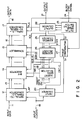
- the present invention relates to a digital multiplexer for time-division multiplexing digital signals from framing units.
- a digital multiplexer is a device for converting lower-order group input signals, which are asynchronous digital signals, on a plurality of channels to a higher-order group signal by time-division multiplexing.
- a conventional digital multiplexer is described in "Multiplexing and Synchronization Techniques," ch.3 in a book entitled “Digital Communication Techniques,” Tokai University publishing society in Japan.
- this digital multiplexer a plurality of framing units are provided for a plurality of channels, respectively, and output signals of the framing units are time-division multiplexed by a multiplexer.
- the multiplexer provides to the framing units block synchronization signals each of which is delayed in time by a predetermined number of bits which differs from channel to channel.
- Each of the framing units produces a block signal composed of a m-bit information signal and a 1-bit block delimiter signal in synchronism with a corresponding block synchronization signal.
- the multiplexer multiplexes block signals sequentially sent from the framing units and adds C bits to a resultant multiplexed signal. This results in a BSI-code higher-order group signal composed of mBlC.
- the multiplexer needs delay circuits corresponding in number to the channels. This will result in increased scale and cost of the multiplexer circuitry.
- delay circuits necessary for producing block synchronization signals must be provided in the number of signals to be multiplexed. This will render flexible alteration of the number of signals to be multiplexed difficult.
- N framing units block N-channel digital information signals, respectively, to provide blocked signals.
- the framing units respond to a common block synchronization signal from a multiplexing unit to provide the blocked signals in a time relation suitable for multiplexing.
- the multiplexing unit multiplexes the blocked signals from the framing units to provide a multiplexed signal (higher-order group signal).
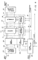
- a digital multiplexer of the present invention comprises N framing units 2 connected to receive lower-order group signals l on N channels, respectively, and having their outputs coupled to a multiplexing unit 5.
- a lower-order group input signal is converted by a corresponding framing unit to a blocked signal 3 composed of m-bit information and a l-bit block delimiter signal inserted at (m+l)-bit intervals.
- Blocked signals from framing units l are then time-division multiplexed by multiplexing unit 5 for conversion to a higher-order group signal of a BSI (Bit Sequence Independence) code 6 of mBl, for example.
- BSI Bit Sequence Independent
- mBl is a coded signal composed of a m-bit information signal (m-l bits in the case of a block containing a control bit) and a C (Complementary) bit serving as the block delimiter bit having a cycle of m+l bits
- mBl is a coded signal composed of a m-bit information signal (m-l bits in the case of a block containing a control bit) and a C (Complementary) bit serving as the block delimiter bit having a cycle of m+l bits
- the C bit is represented by a complement of an information bit k bits before. Namely, if the information bit preceding the C bit by k bits is l, then the C bit will be 0. Conversely, if the information bit is 0, then the C-bit will be l.
- the higher-order group signal 6 resulting from the multiplexing process will never contain consecutive 1s or 0s more than m bits and thus has a proper format for the BSI code.
- a complement of the information bit of the previous channel may be used.
- the block delimiter signal for each channel of the higher-order group signals may be replaced by a complement of an information bit k bits before.
- a space bit or a mark bit may be used as the block delimiter signal.
- the insertion of the block delimiter signal, or the C bit into a blocked signal may be performed by either of framing unit 2 and multiplexing unit 5.
- Framing units 2 are arranged to receive a common block synchronization signal 4 from multiplexing unit 5, delay the respective data by the respective necessary bits and deliver blocked signals 3 simultaneously.
- Multiplexing unit 5 converts the N-bit parallel signal to a serial signal, thereby producing a time-division multiplexed higher-order group signal.
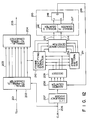
- Fig. 2 shows a detailed arrangement of framing units of Fig. 1.
- a serial-to-parallel converter 12 has an input terminal and m data output terminals. Input data 11 applied to the input data terminal in serial form constitutes a digital information signal which corresponds to the lower-order group signal of Fig. 1.
- serial-to-parallel converter 12 produces parallel data of m-n bits, m-n bits (m-l bits in this embodiment) are output onto the first to (m-n)-th or (m-l)-th output lines in the embodiment.
- serial-to-parallel converter 12 applies the parallel data to bit inserter 14 via the output lines.
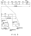
- bit inserter 14 provides to a remaining output line of converter 12 control bits including, as shown in Fig. 3, frame synchronization bits (F1-F4) necessary for framing, a channel-identifying bit (CID), a parity bit (P), a service bit (SV), staff control bits (SFC1 - SCF3), a staff bit (SB) and the like.
- F1-F4 frame synchronization bits necessary for framing
- CID channel-identifying bit
- P parity bit
- SV service bit
- SFC1 - SCF3 staff control bits
- SB staff bit
- Frame synchronization bits F1 to F4 are used for specifying the position of a corresponding frame at the receiving end, in other words, for establishing frame synchronization.
- Channel identification bit CID is used for identifying a corresponding channel to which the relevant frame belongs.
- Parity bit P is used for parity check at the receiving end.
- Service bit SV is at user's disposal. Parity bit P may be inserted into the parallel data after the multiplexing process to higher-order group signal 6.
- Staff bit SB is provided for synchronization of the input and output of framing unit 2 and inserted into a specific position when a phase difference above a fixed value occurs between input and output clocks.
- Staff control bits SFC1 to SFC3 are adapted to represent whether data at a position into which the staff bit is to be inserted is staff bit SB or usual data. The insertion of staff bit SB into the parallel data is called "staff on.”
- bit inserter 14 Outputs of bit inserter 14 are connected to a scrambler 15.
- Scrambler 15 scrambles an output signal of bit inserter 14 so as to keep the mark-to-space ratio of the output signal almost constant and then provides a parallel frame signal 16.
- bit inserter 14 and scrambler 15 constitute the framing unit.
- Outputs of the framing unit, or outputs of scrambler 15 are connected to inputs Of a parallel-to-serial converter 17.
- Parallel-to-serial converter 17 converts the parallel frame signal 16 from the framing unit to a serial data signal which in turn is output as a block signal 18.
- Input clocks (a first clock signal) 19 are applied to serial-to-parallel converter 12 and an input counter (a first counter) 20 through a clock input terminal.
- the input clocks 19 are synchronized with input data 11.
- Input counter 20 serves as means for switching the parallel data 13 output from serial-to-parallel converter 12 between m bits and (m-n) bits and is composed of a modulus counter of dividing-factor variable type.
- Input counter 20 usually operates as a modulo m counter to apply a latch pulse LAP to serial-to-parallel counter 12 when counting the input clocks 19 by m, i.e., the number of bits contained in the parallel data 13.
- output clocks (a second clock signal) 21 are applied to parallel-to-serial converter 17, an output counter 22 and a phase comparator 27 through an output clock terminal.
- the output clocks are synchronized with the output data 18.
- Output counter 22 is a modulo (m+l) counter which is adapted to produce internal clocks (a third clock signal) ICK used in bit inserter 14 and scrambler 15 and apply a parallel load signal PLS to parallel-to-serial converter 17 when the count thereof becomes 0.
- the parallel load signal PLS is used as a timing signal for outputting the block signal 18 from parallel-to-serial converter 17.
- Output counter 22 is connected to an initial-value setting switching circuit 23. Supplied with a block synchronization signal 24 corresponding to the block synchronization signal 4 produced by multiplexing unit 5 of Fig. 1, initial-value setting circuit 23 loads an initial value previously set therein to output counter 22. Output counter 22 is preset by the initial value and issues to serial-to-parallel converter 17 the parallel load signal PLS corresponding to the initial value. Accordingly, the phase of the parallel load signal PLS, acting as the timing signal for outputting the block signal 18, can arbitrarily be set to the block synchronization signal 24 by selection of the initial value. Thus, it becomes possible to control the output timing of the block signal 18, or the phase of the block signal relative to the block synchronization signal 24. As a result, even if being supplied with the common block synchronization signal 4, framing units 2 of Fig. 1 can simultaneously issue the block signals 3 so that they may correctly be multiplexed in multiplexing unit 5, by properly setting initial-value setting switch 23.
- the internal clocks ICK produced by output counter 22 are applied to bit inserter 14, scrambler 15 and address counter 25.
- Outputs of address counter 25 are coupled to inputs of phase comparator 27 along with an output of phase comparator 27.
- Phase comparator 27 makes a comparison between a phase-comparing signal S1 issued from input counter 20 and a phase reference signal S2 issued from output counter 22.
- Phase reference signal S2 has only to be synchronized with the output clocks 21. Thus, for example, even a start pulse in one frame may be used as the phase synchronization signal.
- Phase comparator 27, having a storage function stores the result of the phase comparison between signals S1 and S2 at a specific time within one frame. When detecting phase inconsistency of signals S1 and S2 and storing its comparison result, phase comparator 27 issues a staff demand signal SFTR to address decoder 26.
- a time when phase comparator 27 stores the comparison result is a time earlier than the first bit SFC1 of staff control bits SFC1 to SFC3 (Fig. 3), for example, a time corresponding to the front position of a frame. This is because, when address decoder 26 receives the staff demand signal SFTR from phase comparator 27, each of the staff control bits SFC1 to SFC3 is set to a specific value, and whether or not the staff bit SB is to be inserted into the block signal is instructed by a combination of the three bits.
- phase comparator 27 When phase comparator 27 is timed to store the comparison result as described above, the setting of the staff bits SFC1 to SFC3 and the insertion of the staff bit SB into the block signal on the basis of the stored comparison result may be performed in the same frame as the frame in which the comparison result is recorded.
- Phase comparator 27 may store the comparison result later than the first staff control bit SFC1. Not only is the comparison result stored once per one frame, but also it may be stored several times per one frame in synchronism with the cycle of blocks forming one frame. In this case, setting of the staff control bits SFC1 to SFC3 and insertion of the staff bit SB may be performed in the next frame. The storage of the comparison result in phase comparator 27 is cancelled within a period of time between the insertion of the staff bit SB based on the storage and the completion of framing the relevant frame.
- Address decoder 26 responds to the outputs of address counter 25 and the output of phase comparator 27 to apply a select signal to an insert data selector 28, an insert control signal INS-C to bit inserter 14, a scramble off signal SCR-O and a scramble reset signal SCR-R to scrambler 15, and a counter mode switching signal CNT-C to input counter 20.
- the counter mode switching signal CNT-C is adapted to switch input counter 20 from the modulo m counter to the modulo (m-l) counter when bit inserter 14 inserts data to be inserted (control signal) from insert data selector 28 in the parallel data 13.
- input counter 20 issues the latch pulse LAP to serial-to-parallel converter 12 after counting (m-l) input clocks 19.
- serial-to-parallel converter 12 issues parallel data of input data 11 onto only (m-l) output lines among m output lines and no data onto another output line.
- the output line with no data can be used as an empty bit for bit inserter 14.
- bit inserter 14 can apply a control bit to the empty-bit output line.
- the output line used as the empty bit is preselected to be the lowermost one (the m-th output line) of the output lines of serial-to-parallel converter 12.
- Bit inserter 14 inserts in this empty bit a control bit necessary for framing supplied from insert data selector 28.
- address counter 25 address decoder 26 and insert data selector 28 constitute a frame controller.
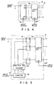
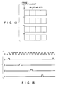
- Fig. 4 shows an arrangement of serial-to-parallel converter 12, which is comprised of an m-stage shift register 41 and a latch circuit 42.
- M-stage shift register 41 receives input data (lower-order group signal) 11 and input clocks 19, and latch circuit 42 responds to latch pulse LAP to temporally store parallel outputs of shift register 41 and issue parallel data 13.
- Fig. 5 shows another arrangement of serial-to-parallel converter 12, which is comprised of m edge-triggered type-D flip-flops 51, a latch circuit 52 responsive to latch pulse LAP to temporally store outputs of flip-flops 51, a counter 53 adapted to count input clocks 19, and a decoder 54 for decoding an count of counter 53.
- Fig. 6 shows waveforms of outputs Qcl through Qcm of decoder 54 which are applied to clock inputs of flip-flops 51 as clock pulses. By being sequentially clocked, flip-flops 51 can operate like shift register 41 of Fig. 4.
- a master-slave type-D flip-flop may be used as each of flip-flops 51 of Fig. 5.
- the clock pulses provided by decoder 54 are such that their rising edges are sequentially delayed and their falling edges occur simultaneously as shown in Fig. 7.
- Master flip-flops respond to the rising edges of the clock pulses to perform serial-to-parallel conversion of input data 11.
- slave flip-flops latch the parallel data from the master flip-flops in response to the falling edges of the clocks.
- flip-flops (master-slave flip-flops) 51 double as latch circuits, eliminating the need for latch circuit 52.
- Fig. 8 specifically shows the output signals of address decoder 26 responsive to output signals of address counter 25 and the insert data 29 applied to insert data selector 28.
- F1 ⁇ F4, SV, CID, P, SFC1 ⁇ SFC3 applied to insert data selector 28 from address decoder 26 instruct selection of corresponding control signals denoted by the same symbols in Fig. 3.
- F1D ⁇ F4D, SVD, CIDD, PD, SBD, SFC1D ⁇ SF3D contained in the insert data 29 each represent a value of data to be inserted in the parallel data 13 as a corresponding one of the control signals F1 ⁇ F4, SV, CID, P, SFC1 ⁇ SFC3.
- the insert control signal INS-C issued from address decoder 26 is used for instructing bit inserter 14 of the presence or absence of insert data.
- the scramble-off signal SCR-O is used to instruct whether the m-th line data of parallel data applied to scrambler 15 should be scrambled or not (scramble-off). When a control signal is on the m-th line, the scramble-off state results.
- the scramble reset signal SCR-R is used to reset a random sequence generator (to be described later) in scrambler 15.
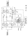
- the parallel data 13 from serial-to-parallel converter 12 is applied to m edge-triggered type-D flip-flops 61, serving as buffers, which latch the parallel data in response to the rising edge of a clock obtained through an inverter 62 for inverting internal clocks ICK.
- Outputs of flip-flops 61 are latched by m edge-triggered type-D flip-flops 63 which respond to the rising edge of a clock obtained through a buffer 64 connected to receive internal clocks ICK.
- a switch 65 is inserted between the Q output of the m-th flip-flop 61m and the D input of the m-th flip-flop 63m.
- This switch 65 is controlled by the Q output of an edge-triggered type-D flip-flop 66 which is responsive to the rising edge of an output clock of inverter 62 to latch the insert control signal INS-C.
- Switch 65 normally connects the Q output of flip-flop 61m with the D input of flip-flop 63m.
- switch 65 disconnects flip-flop 61m from flip-flop 63m to apply insert data selected by insert data selector 28 to the D input of flip flop 63m as a control signal. Consequently, the control signal is inserted into the previous empty bit.
- a block diagram of scrambler 15 is shown.
- the parallel data from bit inserter 14 is applied to m edge-triggered type-D flip-flops 71, serving as buffers, which latch the parallel data in response to the rising edge of a clock obtained through an inverter 72 for inverting internal clocks ICK.
- Outputs of flip-flops 71 are coupled to inputs of m exclusive OR circuits (EOR circuits) 73, respectively.
- EOR circuits 73 have their other inputs connected to outputs of quasi-random generator 74.
- EOR circuits 73 are applied to m edge-triggered type-D flip-flops 75 which latch the EOR-circuit outputs in response to the rising edge of a clock obtained through a buffer 76 for inverting internal clocks ICK.
- Quasi-random generator 74 generates m M-sequence (maximum periodic sequence) signals. When the quasi-random sequential signal and input data are exclusively ORed, the input data is randomized, in other words, scrambled.
- a switch 77 is inserted between the input/output of the m-th EOR circuit 73m and the D input of the m-th flip-flop 75m.
- This switch 77 is controlled by the Q output of an edge-triggered type-D flip-flop 78 which is responsive to the rising edge of an output clock of inverter 72 to latch the scramble-off signal SCR-O.
- Switch 65 normally connects the output of EOR 73m with the D input of flip-flop 75m. When the scramble-off signal SCR-O comes into the scramble-off state, switch 65 connects the input of EOR circuit 73m (the output of flip-flop 71m) to the D input of flip-flop 75m.
- the first through (m-l)-th bits of the parallel data from bit inserter 14 are normally scrambled, while the m-th bit is scrambled only when an information signal (input data) is on the m-th bit line.
- an information signal is on the m-th bit line, the information signal is issued as it is without being scrambled.
- Quasi-random generator 74 is formed of an array of shift registers and an exclusive OR circuit for feedback connection from proper stages of each shift register to the input thereof, generating a quasi-random pattern which is repeated in a long cycle.
- quasi-random generator 74 is reset by application of scramble reset signal SCR-R thereto so as to return the output thereof to an initial value and initiate the generation of the quasi-random sequence signals in a sequence determined by the feedback connection again.
- the initial value of quasi-random generator 74 can be set by initial value setting switch 79. If the initial value is made different from framing unit to framing unit of the digital multiplexer of Fig. 1, the randomization would not be degraded even after the multiplexing process by multiplexing unit 5.
- each of the framing units respond to the common frame synchronization signal from the multiplexing unit to produce a train of blocked signals
- the train of blocked signals of each framing unit is delayed from the train of blocked signals of the following framing unit by a time corresponding to a predetermined number of bits between successive blocked signals.
- Multiplexing unit 5 multiplexes the blocked signals from framing units 2 to produce a multiplexed signal (higher-order group signal). That is to say, framing units 2 perform the delay process necessary for multiplexing, and multiplexing unit 5 multiplexes the blocked signals simultaneously sent from framing units 2 to provide the higher-order group signal. Therefore, multiplexing unit 5 needs no delay circuits.
- each of framing units 2 performs both the insertion of control information necessary for framing and the staff process for synchronization. Therefore, the circuit scale of the multiplexer of the present invention can considerably be reduced as compared to a prior art which performs the framing process and the staff process separately.
- the framing process is performed at a stage in which the input data is converted to the parallel data of m bits or (m-l) bits by serial-to-parallel converter 12. Therefore, even if the bit rate of the lower-order group signal, or input data 11 is high, the processing speed for framing may be l/m or l/(m-l) Of the bit rate. This permits the use of general-purpose inexpensive electronic components in portions other than serial-to-parallel converter 12 and parallel-to-serial converter 17.
- the serial input data is converted by the serial-to-parallel converter to the parallel data of m bits or (m-n) bits (m>n>0) for the m output lines or (m-n) output lines, exclusive of n output lines in specific positions, and the control bits necessary for framing are put onto the n output lines (in the case of the parallel data of m-n bits) for insertion in the parallel data.
- the parallel data is converted to the serial data by the serial-to-parallel converter.
- the lowered processing speed is accompanied by reduced influence of propagation delay of the control signals on the framing unit.
- inside layouts of ICs will not be almost subjected to limitations for reducing the propagation delay.
- an input terminal receiving serial input data 101 is connected to an input terminal of a serial-to-parallel converter 102, and a frame controller 105 is connected to a tag word memory 107.
- Serial-to-parallel converter 102 converts the serial input data 101 to parallel data 103 of m bits for application to data memory 104.
- Data memory 104 stores the parallel data 103.
- tag word 106 of n bits generated from frame controller 105 is written into a tag memory 107.
- Data memory 104 and tag memory 107 may be formed integrally by a (m+n)-bit memory.
- Serial-to-parallel converter 102 is comprised of a m-bit shift register. What number of bits (k bits, m ⁇ k) of the m-bit output are to be used is determined by the time when a write pulse 108 is applied from frame controller 105 to data memory 104 and tag memory 107. That is, if the write pulse is applied to the memory at the instant of entry of the k-th bit of serial input data 101 into shift register 102, then k-bit data is written into data memory 104 as parallel data 103.
- Frame controller 105 responds to input clocks 109 synchronized with input data 101 and output clocks 110 synchronized with output data 121 to produce write pulse 108 and processing clocks 118 to be described later.
- Frame controller 105 includes a counter for counting the clocks and a memory accessed by the count value of the counter, to output the tag word.
- Tag word 106 carries information concerning processes to be executed by processing units 111 and 115.
- Inserter 111 is externally supplied with a block synchronization bit, a parity bit, a service bit, a staff control bit, a staff bit and so on as control bits 114 to be added to parallel data 103 and inserts control bits 114 in (m-k) bits of parallel data 103 in accordance with the decode result for the first bit of the tag word from memory/decoder circuit 113.
- Parallel data issued from first processing unit 111 is transferred to scrambler 116 in second processing unit 115, and, at the same time, outputs of memory/decoder 113 of first processing unit 111 are transferred to memory/decoder 117 of second processing unit 115.
- scrambler 116 performs an exclusive OR operation of the input parallel data and quasi-random sequential data of M sequences (maximum periodic sequences) output in parallel from a quasi-random generator.
- scrambler 116 operates not to scramble the control bits inserted by inserter 112.
- the scramble control signal may be used to instruct the presence or absence of the scramble reset.
- the output of the quasi-random generator is reset to 0 in scrambler 116.
- parallel data (parallelly framed data) 119 is returned to serial data by parallel-to-serial converter 120 and then transferred to a multiplexing unit or a transmission system as output data 121 of the framing unit.
- First and second processing units 111 and 115 perform transfers of the parallel data and tag word and internal processes in synchronism with processing clocks 118 from frame controller 105.
- the transfers of the parallel data and tag word could reliably be performed by displacing the phase of processing clocks by 180 degrees or 90 degrees.
- processing clocks 118 two-phase clocks ⁇ 1 and ⁇ 2 differing in phase by 180 degrees as shown and four-phase clocks sequentially displaced in phase by 90 degrees may be used.
- Processing clocks 118 are generally generated in correlation with output clocks 110. In other words, processing clocks 118 are generated in the same cycle as output clocks 110.
- the processing units may include processing units for performing the alteration of data and the like which have no direct correlation with the framing.
- processing units for performing the alteration of data and the like which have no direct correlation with the framing.
- a tag word with information associated with the processes to be performed as well as parallel data may be transferred.
- the tag word need not be in one-to-one correspondence with the above processes.
- the tag word may be assigned a binary code representing the number of times of conversion from the front of a frame in serial-to-parallel converter 102, in other words, a word number (block number) of parallel data 103 obtained by serial-to-parallel converter 102.
- the binary code is initialized at the front of the frame.
- each processing unit can determine what process to perform in a block known from the block number on the basis Of the decode result by the decoder circuit, and executes subsequent processing based on the determined result.
- frame controller 105 issues tag word data directing the framing process which is transferred to memory/decoder circuits 113 and 117 via tag memory 107.
- inserter 112 and scrambler 116 perform their own unique processes according to the contents of the tag word decoded by memory/decoder circuits 113 and 117, or the insertion of the control bits and the scrambling process.
- input data 101 is formatted in a form suitable for the framing process by frame controller 105 and then transferred to processing units 111 and 115 together with the tag word data.
- Processing units 111 and 115 process the input data in accordance with the tag word. Therefore, processing units 111 and 115 can uniquely process the input data without being controlled by the input data.
- serial input data is converted to parallel data and stored in the data memory, and then the parallel data read from the image memory is sequentially subjected to different types of process necessary for the framing.
- the processing speed can be lowered by a factor corresponding to the number of bits of the parallel data, and the framing can be realized by using low-speed components in various portions except for the serial-to-parallel and parallel-to-serial converters.
- a problem of a time difference between the parallel data and the tag word will not virtually arise because the tag word carrying information directly or indirectiy concerning the processes to be performed by each processing unit is stored in the tag memory and then sequentially transferred to the processing units simultaneously with the parallel data stored in the data memory. Accordingly, in the case of IC version of the apparatus, the inside layout of an IC can be made free from such limitations for timing adjustment of control operations and data signals as in the prior art, enabling a layout with high degree of freedom to be designed.
- n 8 bits.
- input data 201 is serial data which has a bit rate of and a frame structure in which one block is comprised of 8 bits and frame identifying signals F1, F2, F3, F4 are each added to the front of a first block of four successive blocks as shown in Fig. 13.
- the serial data is converted to 8-bit parallel data 203 by serial-to-parallel converter 202.
- the frame synchronizing signal is issued onto the lowest one of 8 output lines of serial-to-parallel converter 202.
- Output data 203 of serial-to-parallel converter 202 is returned to serial data 205 by parallel-to-serial converter 204 and then sent to a succeeding circuit.
- the clock signal a is applied to address counter 208 serving as a first counting means.
- Output signals of address counter 208 are applied to decoder circuit 209 to provide 4-phase sequential pulses (frame position pulses) shown at b, c, d, e in Fig. 14 and having the same period as the frame identifying signal. That is, a frame position pulse is produced once every four blocks.
- the frame position pulses are entered into frame identifying signal detector 210 and frame pattern generator 211.
- Frame identifying signal detector 210 detects a frame identifying signal on the specific bit of parallel data 203 from serial-to-parallel converter 202 by using the frame position pulses.
- Frame pattern generator 211 ANDS the frame position pulses with a frame identifying bit previously set to provide a frame pattern.
- Coincidence detector 212 detects the coincidence or inconsistency between the frame identifying signal from frame identifying circuit 210 and the frame pattern from frame pattern generator 211 to produce a coincidence detect pulse 213 when the coincidence occurs or an inconsistency detect pulse 214 when no coincidence occurs.
- Frame protection counter 215 serving as second counting means comprises modulo l counter 216, modulo m counter 217 and JK flip-flop 218.
- Counters 216 and 217 are adapted to detect coincidence detect pulse 213 and inconsistency detect pulse 214, respectively.
- Counter 216 for counting coincidence detect pulse 213 is reset by inconsistency detect pulse 214
- counter 217 for counting inconsistency pulse 214 is reset by coincidence detect pulse 213.
- Outputs of counters 216 and 217 are coupled to J and K inputs, respectively, of flip-flop 218 which provides a count enable signal 219 to address counter 208.
- flip-flop 218 is inverted in state to temporally disable address counter 208 so that a synchronization restorative operation is performed.
- the frame synchronization is established only when coincidence detect pulse 213 is successively produced for eight frame periods. The synchronization will not be lost unless inconsistency detect pulse 214 is successively produced over eight frames.
- the frame synchronization pulse may be produced on the basis of coincidence detect pulse 213 from coincidence detector 212.
- serial input data having a frame structure in which a frame identifying signal is located at a predetermined position of blocks
- parallel data is converted to parallel data in such a way that the frame identifying signal always appears in a specific bit, and then the detection of the frame identifying signal is performed for the specific bit.
- the circuit scale can be reduced significantly.
- the frame synchronization circuit can be realized by using general-purpose ICs instead of using high-speed logic components because the transmission signal is lowered in speed by the serial-to-parallel conversion to establish the frame synchronization.
Claims (19)
- Unité de formation de trames utilisée pour un multiplexeur numérique, caractérisée en ce qu'elle comprend :
un moyen de conversion de série en parallèle (12) ayant m lignes de sorties parallèles, pour convertir une donnée d'entrée série en une donnée parallèle de m bits ou de (m - n) bits (m > n > 0) et pour sortir la donnée parallèle sur m ligne de sortie ou sur (m - n) lignes de sorties à l'exclusion de n lignes de sorties spécifiques ;
un moyen de commutation (20) pour commuter de manière sélective la donnée parallèle sortie par ledit moyen de conversion de série en parallèle (12) entre n bits et (m - n) bits ;
un moyen de formation de trames (14, 15) pour insérer des bits de commande nécessaires pour la formation de trames dans lesdites n lignes de sortie spécifiques lorsque la donnée parallèle de (m - n) bits est sortie dudit moyen de conversion de série en parallèle ; et,
un moyen de conversion de parallèle en série (17) pour convertir la donnée de sortie dudit moyen de formation de trames en donnée série. - Unité de formation de trames selon la revendication 1, caractérisée en ce que ledit moyen de formation de trame comprend un moyen (14) pour insérer de manière sélective un bit de synchronisation de trame, un bit d'identification de canal, un bit de parité, un bit de service et au moins l'un d'un bit de commande de repérage de déphasage et d'un bit de repérage de déphasage.
- Unité de formation de trames selon la revendication 1, caractérisée en ce que ledit moyen de formation de trames comprend un moyen (15) pour crypter la donnée parallèle.
- Unité de formation de trames selon la revendication 1, caractérisée en ce que,
ledit moyen de conversion de série en parallèle (12) possède une fonction de registre à décalage pour décaler la donnée d'entrée série, en réponse à des signaux d'horloge prédéterminés, et une fonction de verrou ; et caractérisée en ce que,
ledit moyen de commutation comprend un moyen de comptage (20) pour compter les impulsions d'horloge et possédant un facteur de division commutable entre 1/m et 1/(m+1), ledit moyen de comptage appliquant une impulsion de verrouillage audit moyen de conversion de série en parallèle pour commuter de manière sélective ladite donnée parallèle qui en est issue entre m bits et (m - n) bits. - Multiplexeur numérique comprenant :
N unités de formation de trames (2) pour mettre sous forme de blocs des signaux d'information numérique de N canaux en fonction d'un format approprié pour la formation de trames, pour fournir N signaux sous forme de bloc comportant chacun un certain nombre de signaux de bloc, caractérisé en ce qu'il comprend en outre :
un moyen de multiplexage (5) pour produire un signal de synchronisation de bloc et pour multiplexer par répartition dans le temps les signaux de bloc sortis simultanément desdites unités de formation de trames, au moins un à la fois, en réponse au signal de synchronisation de bloc pour fournir un signal multiplexé par répartition dans le temps ;
chacune desdites unités de formation de trames (2) incluant un moyen de production de signal de cadencement (22, 23) sensible au signal de synchronisation de bloc pour produire un signal de cadencement à un instant fonction d'une valeur initiale qui diffère d'une unité de formation de trames à l'autre ; et un moyen (17) pour produire le signal de bloc en synchronisme avec le signal de cadencement. - Multiplexeur numérique selon la revendication 5, caractérisé en ce que ledit moyen de production de signaux de cadencement comprend un moyen de réglage de valeur initiale (23) ; un moyen de comptage (22) pour compter les signaux d'horloge appliqués de l'extérieur pour produire le signal de cadencement lorsque le comptage des signaux d'horloge dont le nombre correspond à la valeur initiale fixée par ledit moyen de réglage de valeur initiale (23) en réponse au signal de synchronisation de bloc.
- Multiplexeur numérique selon la revendication 5, caractérisé en ce que chacune desdites unités de formation de trames (2) comprend un moyen de conversion de série en parallèle (12) pour convertir le signal d'information numérique en donnée parallèle ; un moyen de formation de trame (14, 15) pour ajouter de manière sélective une information binaire spécifique à la donnée parallèle issue dudit moyen de conversion de série en parallèle pour fournir un signal de trame parallèle incluant le signal de bloc ; et un moyen de conversion de parallèle en série (17) pour convertir le signal de trame parallèle issue dudit moyen de formation de trames, en donnée série et pour fournir un signal de bloc en réponse au signal de cadencement.
- Unité de formation de trames utilisée pour un multiplexeur, caractérisée en ce qu'elle comprend :
un moyen de conversion de série en parallèle (102) pour convertir une donnée d'entrée série en une donnée parallèle ;
une mémoire de données (104) pour mémoriser la donnée parallèle issue du moyen de conversion de série en parallèle ;
un moyen de formation de trames comportant une pluralité d'unités de traitement (111, 115) pour appliquer de manière séquentielle une pluralité de traitements nécessaires pour mettre sous forme de trames les données parallèles lues dans ladite mémoire de données ;
une mémoire d'étiquette (107) pour mémoriser un mot étiquette comportant une pluralité de bits avec de l'information liée à un traitement à appliquer à la donnée parallèle dans chacune desdites unités de traitement ; et,
un moyen (105) pour transférer de manière séquentielle le mot étiquette auxdites unités de traitement (111, 115) dans ladite unité de formation de trame. - Unité de formation de trames, selon la revendication 8, caractérisée en ce que ledit moyen de formation de trames, comprend une unité de traitement (112) pour ajouter des bits de commande nécessaires pour mettre sous forme de trames les données parallèles ; et dans laquelle le mot étiquette contient de l'information pour indiquer la présence ou l'absence de l'insertion des bits de commande pour chaque donnée parallèle.
- Unité de formation de trames selon la revendication 8, caractérisée en ce que ladite unité de formation de trames comprend une unité de traitement (116) pour crypter la donnée parallèle ; et caractérisée en ce que le mot étiquette contient de l'information pour indiquer la manière de crypter pour chaque donnée parallèle.
- Unité de formation de trames selon la revendication 8, caractérisée en ce que les bits du mot étiquette correspondent, respectivement, aux traitements à effectuer par lesdites unités de traitement (111, 115).
- Unité de formation de trames selon la revendication 8, caractérisée en ce que le mot étiquette contient de l'information représentant le nombre de conversions à partir du début d'une trame par ledit moyen de conversion de série en parallèle.
- Unité de formation de trames selon la revendication 8, caractérisée en ce que chacune desdites unités de traitement (111, 115) dans ledit moyen de formation de trames comprend un moyen (113, 117) pour décoder le mot étiquette.
- Unité de formation de trames utilisée pour un multiplexeur numérique, caractérisée en ce qu'elle comprend un moyen de conversion de série en parallèle (12) pour convertir des données d'entrée série en données parallèles, en réponse à des premiers signaux d'horloge ;
un premier moyen de comptage (20) pour compter les premiers signaux d'horloge ;
un second moyen de comptage (22) pour compter des seconds signaux d'horloge ;
un moyen de comparaison de phase (27) pour comparer un signal de sortie dudit premier moyen de comptage (20) avec un signal synchronisé avec les seconds signaux d'horloge ;
un moyen de formation de trames (14, 15, 25, 26, 28), pour mettre sous forme de trame la donnée parallèle provenant dudit moyen de conversion de série en parallèle en synchronisme avec un signal de sortie dudit second moyen de comptage (22) et pour effectuer un traitement de repérage de déphasage en fonction d'une sortie dudit moyen de comparaison de phase (27) ; et,
un moyen de conversion de parallèle en série (17) pour convertir la donnée de sortie dudit moyen de formation de trames en réponse au second signal d'horloge. - Unité de formation de trames selon la revendication 14, caractérisée en ce que ledit moyen de formation de trame comprend un moyen (14) pour insérer de manière sélective, dans des bits spécifiques de la donnée parallèle issue dudit moyen de conversion de série en parallèle (12), au moins l'un d'un bit de synchronisation de trame, d'un bit d'identification de canal, d'un bit de contrôle de parité et d'un bit de service, et un bit de commande de repérage de déphasage et un bit de repérage de déphasage.
- Unité de formation de trames selon la revendication 15, caractérisée en ce que ledit moyen de formation de trames, comprend un moyen (26) pour mémoriser un résultat de comparaison par ledit moyen de comparaison (27) à un instant prédéterminé dans une trame ; et un moyen (28) pour déterminer une valeur du bit de commande de repérage de déphasage en fonction du résultat de comparaison mémorisé et pour insérer le bit de repérage de déphasage dans la donnée parallèle en fonction de la détermination de la valeur du bit de commande de repérage de déphasage.
- Unité de formation de trames selon la revendication 16, caractérisée en ce que le cadencement de mémorisation du résultat de comparaison par ledit moyen de comparaison de phase (27) est réglé à un instant synchrone avec une période de chacun des blocs formant une trame.
- Unité de formation de trames selon la revendication 16, caractérisée en ce que ledit moyen de formation de trames comprend un moyen (28) pour annuler la mémorisation du résultat de comparaison dans un intervalle de temps allant de l'insertion du bit de repérage de déphasage, effectuée en fonction du résultat de comparaison, à la fin d'une trame dans laquelle le bit de repérage de déphasage est inséré.
- Circuit de synchronisation de trames utilisé pour un multiplexeur numérique, caractérisé en ce qu'il comprend :
un circuit convertisseur de série en parallèle (202) pour convertir des données d'entrée série, ayant une structure de trame dans laquelle un signal d'identification de trame est inséré dans une position prédéterminée des blocs, en des données parallèles de n bits, de telle façon que le bit d'identification de trame soit placé au droit d'un bit spécifique ;
un moyen (210) pour détecter le signal de détection de trame à partir du bit spécifique de la donnée de sortie dudit circuit convertisseur de série en parallèle ;
un premier moyen de comptage (208) pour compter un signal d'horloge ayant le même rythme que le rythme de codage des données de sortie dudit circuit convertisseur de série en parallèle ;
un moyen (209) sensible audit premier moyen de comptage pour produire des impulsions de position de trame ayant la même période que celle du signal d'identification de trame ;
un moyen (211) sensible aux impulsions de position de trame issues dudit moyen de production d'impulsions pour produire un modèle de trame du même modèle que celui du signal d'identification de trame ;
un moyen de détection de coïncidence (212) pour détecter la coïncidence/non-coïncidence entre le modèle de trame produit par ledit moyen de production de modèles et le signal d'identification de trame pour produire au moins une impulsion de non-coïncidence ; et,
un second moyen de comptage (217) pour compter des impulsions de non-coïncidence consécutives produites par ledit moyen de détection de coïncidence pour arrêter temporairement l'opération de comptage dudit premier moyen de comptage (208) lorsqu'un nombre prédéterminé d'impulsions de non-coïncidence consécutives sont comptées.
Applications Claiming Priority (10)
| Application Number | Priority Date | Filing Date | Title |
|---|---|---|---|
| JP255000/87 | 1987-10-09 | ||
| JP254996/87 | 1987-10-09 | ||
| JP25500087A JPH0197031A (ja) | 1987-10-09 | 1987-10-09 | フレーム処理装置 |
| JP25499987A JPH0612892B2 (ja) | 1987-10-09 | 1987-10-09 | フレーム処理装置 |
| JP254997/87 | 1987-10-09 | ||
| JP254998/87 | 1987-10-09 | ||
| JP62254996A JPH0197032A (ja) | 1987-10-09 | 1987-10-09 | フレーム同期回路 |
| JP25499887A JPH0197029A (ja) | 1987-10-09 | 1987-10-09 | フレーム処理装置 |
| JP25499787A JPH0197033A (ja) | 1987-10-09 | 1987-10-09 | ディジタル多重変換装置 |
| JP254999/87 | 1987-10-09 |
Publications (3)
| Publication Number | Publication Date |
|---|---|
| EP0311448A2 EP0311448A2 (fr) | 1989-04-12 |
| EP0311448A3 EP0311448A3 (en) | 1990-08-01 |
| EP0311448B1 true EP0311448B1 (fr) | 1994-01-19 |
Family
ID=27530284
Family Applications (1)
| Application Number | Title | Priority Date | Filing Date |
|---|---|---|---|
| EP88309416A Expired - Lifetime EP0311448B1 (fr) | 1987-10-09 | 1988-10-07 | Multiplexeur numérique |
Country Status (3)
| Country | Link |
|---|---|
| US (1) | US4899339A (fr) |
| EP (1) | EP0311448B1 (fr) |
| DE (1) | DE3887249T2 (fr) |
Families Citing this family (16)
| Publication number | Priority date | Publication date | Assignee | Title |
|---|---|---|---|---|
| US5144620A (en) * | 1986-09-30 | 1992-09-01 | Nec Corporation | Cross-connection network using time switch |
| CA2024809C (fr) * | 1989-01-09 | 1994-11-01 | Masanori Hiramoto | Appareil de multiplexage et appareil de demultiplexage de signaux numeriques |
| JP2839547B2 (ja) * | 1989-05-02 | 1998-12-16 | 株式会社東芝 | 半導体集積回路装置 |
| US5359605A (en) * | 1989-06-22 | 1994-10-25 | U.S. Philips Corporation | Circuit arrangement for adjusting the bit rates of two signals |
| DE4035438A1 (de) * | 1990-11-08 | 1992-05-14 | Philips Patentverwaltung | Schaltungsanordnung zum entfernen von stopfbits |
| FR2677208B1 (fr) * | 1991-05-27 | 1993-09-24 | Matra Communication | Procede et dispositif d'insertion de voies paquets dans un signal de television a multiplex analogique-numerique. |
| CA2114526A1 (fr) * | 1992-06-29 | 1994-01-06 | Clifford H. Kraft | Systeme de transmission rapide de donnees a multiplexage temporel |
| US6384996B1 (en) * | 1994-10-31 | 2002-05-07 | Samsung Electronics Co., Ltd. | Insertion of ones and zeroes into I-NRZI modulation for magnetic recording apparatus to facilitate head tracking |
| US5907719A (en) * | 1996-01-22 | 1999-05-25 | Cirrus Logic, Inc. | Communication interface unit employing two multiplexer circuits and control logic for performing parallel-to-serial data conversion of a selected asynchronous protocol |
| KR19980040837A (ko) * | 1996-11-29 | 1998-08-17 | 조희재 | 비화채널 수신방법 |
| US6044121A (en) * | 1997-07-22 | 2000-03-28 | Cabletron Systems, Inc. | Method and apparatus for recovery of time skewed data on a parallel bus |
| US6332173B2 (en) * | 1998-10-31 | 2001-12-18 | Advanced Micro Devices, Inc. | UART automatic parity support for frames with address bits |
| US7095758B2 (en) * | 2000-06-16 | 2006-08-22 | Nippon Telegraph And Telephone Corporation | Multiplexing and transmission apparatus |
| US6333893B1 (en) * | 2000-08-21 | 2001-12-25 | Micron Technology, Inc. | Method and apparatus for crossing clock domain boundaries |
| US8514881B2 (en) * | 2007-01-17 | 2013-08-20 | Nippon Telegraph And Telephone Corporation | Digital transmission system and digital transmission method |
| US8074054B1 (en) * | 2007-12-12 | 2011-12-06 | Tellabs San Jose, Inc. | Processing system having multiple engines connected in a daisy chain configuration |
Family Cites Families (4)
| Publication number | Priority date | Publication date | Assignee | Title |
|---|---|---|---|---|
| FR2376572A1 (fr) * | 1976-12-30 | 1978-07-28 | Roche Alain | Circuits de conversion serie-parallele et de multiplexage ou de conversion parallele-serie et de demultiplexage pour des multiplex numeriques |
| JPS58153434A (ja) * | 1982-03-09 | 1983-09-12 | Nec Corp | 多重変換方式 |
| JPS61108286A (ja) * | 1984-10-31 | 1986-05-26 | Iwatsu Electric Co Ltd | 時分割情報伝送装置 |
| EP0220808A3 (fr) * | 1985-08-26 | 1988-05-04 | AT&T Corp. | Multiplexeur pour signaux numériques |
-
1988
- 1988-10-07 US US07/254,847 patent/US4899339A/en not_active Expired - Lifetime
- 1988-10-07 DE DE3887249T patent/DE3887249T2/de not_active Expired - Lifetime
- 1988-10-07 EP EP88309416A patent/EP0311448B1/fr not_active Expired - Lifetime
Also Published As
| Publication number | Publication date |
|---|---|
| US4899339A (en) | 1990-02-06 |
| DE3887249D1 (de) | 1994-03-03 |
| EP0311448A3 (en) | 1990-08-01 |
| DE3887249T2 (de) | 1994-06-16 |
| EP0311448A2 (fr) | 1989-04-12 |
Similar Documents
| Publication | Publication Date | Title |
|---|---|---|
| EP0311448B1 (fr) | Multiplexeur numérique | |
| EP0405761B1 (fr) | Système de synchronisation de groupes de données tramées dans une transmission en série de bits | |
| US4920546A (en) | Frame synchronizing apparatus | |
| EP0334357B1 (fr) | Dispositif pour l'insertion d'impulsion | |
| EP0405760A2 (fr) | Système de synchronisation de groupes de données tramées dans une transmission en série de bits | |
| US5202904A (en) | Pulse stuffing apparatus and method | |
| EP0379384B1 (fr) | Circuit d'ajustement de phase | |
| US5086438A (en) | Signal generating and receiving apparatuses based on synchronous transfer mode | |
| US4573172A (en) | Programmable circuit for series-parallel transformation of a digital signal | |
| US3541524A (en) | Time division communications processor | |
| EP0548649B1 (fr) | Générateur de code DS3 AIS/Repos parallèle | |
| US3557314A (en) | Frame synchronization circuit | |
| EP0409168B1 (fr) | Circuit de mémoire élastique | |
| US6367027B1 (en) | Skew pointer generation | |
| JPH0380646A (ja) | 擬似乱数加算回路 | |
| JPH0197033A (ja) | ディジタル多重変換装置 | |
| JP2548709B2 (ja) | 多重フレ−ムアライナ | |
| JP2577986B2 (ja) | 擬似ランダム雑音符号発生器 | |
| JPH0197031A (ja) | フレーム処理装置 | |
| JPH0197029A (ja) | フレーム処理装置 | |
| JP3309161B2 (ja) | Cidパターン発生装置 | |
| KR970024666A (ko) | 피씨엠 데이타 지연회로 | |
| KR930004309B1 (ko) | 신호 변환회로 | |
| KR100363411B1 (ko) | 그룹간선상의 채널선택 로직회로 | |
| KR890000056B1 (ko) | 시분할 다중 통신 시스템의 데이터 동기회로 |
Legal Events
| Date | Code | Title | Description |
|---|---|---|---|
| PUAI | Public reference made under article 153(3) epc to a published international application that has entered the european phase |
Free format text: ORIGINAL CODE: 0009012 |
|
| 17P | Request for examination filed |
Effective date: 19881014 |
|
| AK | Designated contracting states |
Kind code of ref document: A2 Designated state(s): DE FR GB SE |
|
| PUAL | Search report despatched |
Free format text: ORIGINAL CODE: 0009013 |
|
| AK | Designated contracting states |
Kind code of ref document: A3 Designated state(s): DE FR GB SE |
|
| 17Q | First examination report despatched |
Effective date: 19930422 |
|
| GRAA | (expected) grant |
Free format text: ORIGINAL CODE: 0009210 |
|
| AK | Designated contracting states |
Kind code of ref document: B1 Designated state(s): DE FR GB SE |
|
| PG25 | Lapsed in a contracting state [announced via postgrant information from national office to epo] |
Ref country code: SE Effective date: 19940119 |
|
| REF | Corresponds to: |
Ref document number: 3887249 Country of ref document: DE Date of ref document: 19940303 |
|
| ET | Fr: translation filed | ||
| PG25 | Lapsed in a contracting state [announced via postgrant information from national office to epo] |
Ref country code: GB Effective date: 19941007 |
|
| PLBE | No opposition filed within time limit |
Free format text: ORIGINAL CODE: 0009261 |
|
| STAA | Information on the status of an ep patent application or granted ep patent |
Free format text: STATUS: NO OPPOSITION FILED WITHIN TIME LIMIT |
|
| 26N | No opposition filed | ||
| GBPC | Gb: european patent ceased through non-payment of renewal fee |
Effective date: 19941007 |
|
| PGFP | Annual fee paid to national office [announced via postgrant information from national office to epo] |
Ref country code: DE Payment date: 20071004 Year of fee payment: 20 |
|
| PGFP | Annual fee paid to national office [announced via postgrant information from national office to epo] |
Ref country code: FR Payment date: 20071009 Year of fee payment: 20 |