EP0303193A2 - Integrierte Halbleiterschaltungsvorrichtung - Google Patents
Integrierte Halbleiterschaltungsvorrichtung Download PDFInfo
- Publication number
- EP0303193A2 EP0303193A2 EP88112741A EP88112741A EP0303193A2 EP 0303193 A2 EP0303193 A2 EP 0303193A2 EP 88112741 A EP88112741 A EP 88112741A EP 88112741 A EP88112741 A EP 88112741A EP 0303193 A2 EP0303193 A2 EP 0303193A2
- Authority
- EP
- European Patent Office
- Prior art keywords
- circuit
- boost
- charge pumping
- voltage
- mos transistors
- Prior art date
- Legal status (The legal status is an assumption and is not a legal conclusion. Google has not performed a legal analysis and makes no representation as to the accuracy of the status listed.)
- Granted
Links
- 239000004065 semiconductor Substances 0.000 title claims abstract description 10
- 238000005086 pumping Methods 0.000 claims abstract description 34
- 239000003990 capacitor Substances 0.000 claims abstract description 20
- 230000000875 corresponding effect Effects 0.000 description 10
- 238000010586 diagram Methods 0.000 description 2
- 230000004075 alteration Effects 0.000 description 1
- 230000000694 effects Effects 0.000 description 1
- 238000000034 method Methods 0.000 description 1
- 230000003252 repetitive effect Effects 0.000 description 1
- 230000001360 synchronised effect Effects 0.000 description 1
Images

Classifications
-
- G—PHYSICS
- G11—INFORMATION STORAGE
- G11C—STATIC STORES
- G11C17/00—Read-only memories programmable only once; Semi-permanent stores, e.g. manually-replaceable information cards
-
- H—ELECTRICITY
- H02—GENERATION; CONVERSION OR DISTRIBUTION OF ELECTRIC POWER
- H02M—APPARATUS FOR CONVERSION BETWEEN AC AND AC, BETWEEN AC AND DC, OR BETWEEN DC AND DC, AND FOR USE WITH MAINS OR SIMILAR POWER SUPPLY SYSTEMS; CONVERSION OF DC OR AC INPUT POWER INTO SURGE OUTPUT POWER; CONTROL OR REGULATION THEREOF
- H02M3/00—Conversion of DC power input into DC power output
- H02M3/02—Conversion of DC power input into DC power output without intermediate conversion into AC
- H02M3/04—Conversion of DC power input into DC power output without intermediate conversion into AC by static converters
- H02M3/06—Conversion of DC power input into DC power output without intermediate conversion into AC by static converters using resistors or capacitors, e.g. potential divider
- H02M3/07—Conversion of DC power input into DC power output without intermediate conversion into AC by static converters using resistors or capacitors, e.g. potential divider using capacitors charged and discharged alternately by semiconductor devices with control electrode, e.g. charge pumps
- H02M3/073—Charge pumps of the Schenkel-type
Definitions
- the present invention relates to a semiconductor IC (integrated circuit) device including an internal booster circuit for internally boosting up a power source voltage as supplied from an outer voltage source.
- An electrically erasable, programmable read only memory requires a high voltage of, for example, about 20 V for data alteration and erasure of memory cells.
- a recent EEPROM is designed to internally boost up a power source voltage (usually 5 V) coming from an outer source, not to directly use an external high voltage. Since the user need not prepare any high voltage source, the EEPROM becomes more user-friendly.
- Fig. 1 shows a conventional charge pumping circuit which is employed as an internal booster circuit for EEPROM.
- a plurality of N channel enhancement type MOS (insulated gate type) transistors T1 to Tn are cascade-circuited each having its gate connected directly to its drain.
- a clock signal ⁇ 1 of a first phase is supplied via capacitor C1 to the node of each of the odd-numbered transistors T1 to Tn, while a clock signal ⁇ 2 of a second phase is supplied via capacitor C2 to the node of each of the even-numbered transistors.
- Respective capacitors C1 and C2 have a common capacitive values.
- the clock signals ⁇ 1 and ⁇ 2 are not synchronized with each other and their amplitude level is equal to that of power source voltage V DD , noting that the power source voltage V DD is applied to input voltage node IN.
- Fig. 3 shows a relation between a current output supplied and a boost-up output of the charge pumping circuit. As shown in Fig. 3, a current output supplied becomes very small when the power source voltage V DD is small.
- EEPROMs will be incorporated into a portable electronic apparatus.
- a battery power source of about 3 V is usually employed in that application.
- the conventional internal booster circuit fails to exhibit an adequate current supply capacity.
- a semiconductor integrated circuit device which comprises a first charge pumping circuit comprising a plurality of MOS transistors cascade-connected between an input voltage node and a booster output node with the gate of the MOS transistor connected to the drain thereof, where, of all associated nodes, those odd-numbered nodes receive one of first and second clock signals of a different phase through a corresponding capacitor and those even-numbered nodes receive the other clock signal through a corresponding capacitor; a second charge pumping circuit comprising a plurality of MOS transistors cascade-connected between the input voltage node and the booster output node and equal in number to those of the first charge pumping circuit where, of all associated nodes, those odd-numbered nodes receive one of first and second clock signals of a different phase through a corresponding capacitor and those even-numbered nodes receive the other clock signal through a corresponding capacitor and the gate of the respective MOS transistors is connected to the gate of the corresponding MOS
- the first charge pumping circuit is connected at its output terminal to the high resistive element and hence there is almost no external current loss, it is possible to obtain a considerably high boost-up voltage even if a low-voltage source is employed. Furthermore, the respective stage transistor of the second charge circuit is driven by a voltage on a corresponding stage node of the first charge pumping circuit and hence a high current supply capacity can be obtained from an output terminal of the second charge pumping circuit.
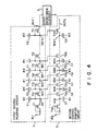
- Fig. 4 shows an internal booster circuit incorporated into a semiconductor circuit, such as an EEPROM.
- 1 and 2 show first and second charge pumping circuits, respectively, with high resistive element 2 connected between a boost-up voltage output node OUT1 of first charge pumping circuit 1 and a ground potential terminal.
- First charge pumping circuit 1 comprises a plurality of MOS transistors T1 to Tn cascade-connected between input voltage node IN1 and output node OUT1 with their gate connected to a corresponding drain.
- Second charge pumping circuit 2 comprises a plurality of MOS transistors T1a to Tna cascade-connected between input voltage node IN2 and booster voltage output node OUT2 and equal to those of first charge pumping circuit 1.
- Clock signals ⁇ 1 and ⁇ 2 are alternately applied, respectively via capacitors C1 and C2, to corresponding ones of nodes N1a to Nna-1 provided between transistors T1a and Tna.
- the gates of transistors T2a ... Tna in second charge pumping circuit 2 are connected to the corresponding gates of transistors T2 ... Tn in first charge pumping circuit 1.
- the same input voltage (usually a power source voltage V DD externally supplied from EEPROM) is applied to input voltage nodes IN1 and IN2 of charge pumping circuits 1 and 2, respectively.
- the gates of first stage transistors T1 and T1a are connected to input voltage nodes IN1 and IN2, respectively, and connected substantially in common with each other.
- the clock signals ⁇ 1 and ⁇ 2 are mutually not so overlapped with respect to each other as in the conventional circuit and have an amplitude level equal to the power source voltage V DD .
- the first charge pumping circuit 1 performs substantially the same operation as the conventional counterpart, but high resistive element 3 is connected to output node OUT1 and hence almost no outer current loss occurs.
- an amount of charge, Q transferred from one transistor to another adjacent one is very small and a voltage V DD - V TH - Q C to be boosted at the respective stage node is nearly equal to V DD - V TH . Since, therefore, there is almost no external current loss, even if an input voltage V DD is as low as, for example, about 3 V, first charge pumping circuit 1 can obtain an adequate boost-up voltage as shown in Fig. 3.
- second charge pumping circuit 2 the gates of transistors T2a ... Tna are connected to the gates of corresponding stage transistors in the first charge pumping circuit, in place of being connected to the drains of transistors T2a ... Tna in the second charge pumping circuit.
- a high gate voltage is applied to the gate of transistors T2a ... Tna as compared to the drain voltage on the side of input voltage node IN2.
- the boost-up voltage at the respective stage becomes V DD - Q C and it is possible to obtain an adequate boost-up voltage output in the case of an amount of charge, Q, being greater, that is, in the case where there is a greater external current loss.
Landscapes
- Engineering & Computer Science (AREA)
- Power Engineering (AREA)
- Dc-Dc Converters (AREA)
- Semiconductor Integrated Circuits (AREA)
- Read Only Memory (AREA)
- Non-Volatile Memory (AREA)
Applications Claiming Priority (2)
| Application Number | Priority Date | Filing Date | Title |
|---|---|---|---|
| JP202387/87 | 1987-08-13 | ||
| JP20238787A JPS6445157A (en) | 1987-08-13 | 1987-08-13 | Semiconductor integrated circuit |
Publications (3)
| Publication Number | Publication Date |
|---|---|
| EP0303193A2 true EP0303193A2 (de) | 1989-02-15 |
| EP0303193A3 EP0303193A3 (en) | 1989-11-15 |
| EP0303193B1 EP0303193B1 (de) | 1993-03-31 |
Family
ID=16456650
Family Applications (1)
| Application Number | Title | Priority Date | Filing Date |
|---|---|---|---|
| EP88112741A Expired - Lifetime EP0303193B1 (de) | 1987-08-13 | 1988-08-04 | Integrierte Halbleiterschaltungsvorrichtung |
Country Status (5)
| Country | Link |
|---|---|
| US (1) | US4935644A (de) |
| EP (1) | EP0303193B1 (de) |
| JP (1) | JPS6445157A (de) |
| KR (1) | KR910007405B1 (de) |
| DE (1) | DE3879804T2 (de) |
Cited By (2)
| Publication number | Priority date | Publication date | Assignee | Title |
|---|---|---|---|---|
| US5196996A (en) * | 1990-08-17 | 1993-03-23 | Hyundai Electronics Industries Co., Ltd. | High voltage generating circuit for semiconductor devices having a charge pump for eliminating diode threshold voltage losses |
| EP0836268A1 (de) * | 1996-10-11 | 1998-04-15 | STMicroelectronics S.r.l. | Verbesserte positive Ladungspumpe |
Families Citing this family (40)
| Publication number | Priority date | Publication date | Assignee | Title |
|---|---|---|---|---|
| JP2533213B2 (ja) * | 1990-02-13 | 1996-09-11 | 株式会社東芝 | 半導体集積回路 |
| US5008799A (en) * | 1990-04-05 | 1991-04-16 | Montalvo Antonio J | Back-to-back capacitor charge pumps |
| KR920006991A (ko) * | 1990-09-25 | 1992-04-28 | 김광호 | 반도체메모리 장치의 고전압발생회로 |
| US5126590A (en) * | 1991-06-17 | 1992-06-30 | Micron Technology, Inc. | High efficiency charge pump |
| CN1075690C (zh) * | 1991-11-07 | 2001-11-28 | 摩托罗拉公司 | 混合信号处理系统及其供电方法 |
| US5191232A (en) * | 1992-03-17 | 1993-03-02 | Silicon Storage Technology, Inc. | High frequency voltage multiplier for an electrically erasable and programmable memory device |
| US5280420A (en) * | 1992-10-02 | 1994-01-18 | National Semiconductor Corporation | Charge pump which operates on a low voltage power supply |
| US5291446A (en) * | 1992-10-22 | 1994-03-01 | Advanced Micro Devices, Inc. | VPP power supply having a regulator circuit for controlling a regulated positive potential |
| US5347172A (en) * | 1992-10-22 | 1994-09-13 | United Memories, Inc. | Oscillatorless substrate bias generator |
| US5337284A (en) * | 1993-01-11 | 1994-08-09 | United Memories, Inc. | High voltage generator having a self-timed clock circuit and charge pump, and a method therefor |
| JP3043201B2 (ja) * | 1993-04-22 | 2000-05-22 | 株式会社東芝 | 昇圧回路 |
| JP2718375B2 (ja) * | 1994-09-30 | 1998-02-25 | 日本電気株式会社 | チャージポンプ回路 |
| JP3638641B2 (ja) * | 1994-10-05 | 2005-04-13 | 株式会社ルネサステクノロジ | 昇圧電位発生回路 |
| US5677645A (en) * | 1995-05-08 | 1997-10-14 | Micron Technology, Inc. | Vccp pump for low voltage operation |
| US5889428A (en) * | 1995-06-06 | 1999-03-30 | Ramtron International Corporation | Low loss, regulated charge pump with integrated ferroelectric capacitors |
| JP2830807B2 (ja) * | 1995-11-29 | 1998-12-02 | 日本電気株式会社 | 半導体メモリ装置 |
| US5734290A (en) * | 1996-03-15 | 1998-03-31 | National Science Council Of R.O.C. | Charge pumping circuit having cascaded stages receiving two clock signals |
| DE69627142T2 (de) * | 1996-08-02 | 2003-10-16 | Stmicroelectronics S.R.L., Agrate Brianza | Bidirektionale Ladungspumpe |
| JPH1145978A (ja) * | 1997-07-28 | 1999-02-16 | Toshiba Microelectron Corp | 半導体記憶装置及び電圧発生回路 |
| US5949708A (en) | 1997-12-31 | 1999-09-07 | Micron Technology, Inc. | Integrated circuit charge coupling circuit |
| US6166982A (en) * | 1998-06-25 | 2000-12-26 | Cypress Semiconductor Corp. | High voltage switch for eeprom/flash memories |
| US6172553B1 (en) | 1998-06-25 | 2001-01-09 | Cypress Semiconductor Corp. | High voltage steering network for EEPROM/FLASH memory |
| US6094095A (en) * | 1998-06-29 | 2000-07-25 | Cypress Semiconductor Corp. | Efficient pump for generating voltages above and/or below operating voltages |
| KR100275743B1 (ko) * | 1998-09-08 | 2001-01-15 | 윤종용 | 승압회로 및 그의 승압방법 |
| US5982224A (en) * | 1998-09-22 | 1999-11-09 | Samsung Electronics Co., Ltd. | Low-power charge pump circuit having reduced body effect |
| US6320797B1 (en) | 1999-02-24 | 2001-11-20 | Micron Technology, Inc. | Method and circuit for regulating the output voltage from a charge pump circuit, and memory device using same |
| US6160723A (en) * | 1999-03-01 | 2000-12-12 | Micron Technology, Inc. | Charge pump circuit including level shifters for threshold voltage cancellation and clock signal boosting, and memory device using same |
| US6037622A (en) * | 1999-03-29 | 2000-03-14 | Winbond Electronics Corporation | Charge pump circuits for low supply voltages |
| JP3476384B2 (ja) * | 1999-07-08 | 2003-12-10 | Necマイクロシステム株式会社 | 昇圧回路とその制御方法 |
| IT1313877B1 (it) * | 1999-12-17 | 2002-09-24 | St Microelectronics Srl | Moltiplicatore di tensione in tecnologia cmos |
| JP3696125B2 (ja) | 2000-05-24 | 2005-09-14 | 株式会社東芝 | 電位検出回路及び半導体集積回路 |
| US7023260B2 (en) * | 2003-06-30 | 2006-04-04 | Matrix Semiconductor, Inc. | Charge pump circuit incorporating corresponding parallel charge pump stages and method therefor |
| JP2005339658A (ja) | 2004-05-26 | 2005-12-08 | Toshiba Corp | 昇圧回路 |
| TWI261407B (en) * | 2004-08-03 | 2006-09-01 | Ememory Technology Inc | Charge pump circuit |
| US7477093B2 (en) * | 2006-12-31 | 2009-01-13 | Sandisk 3D Llc | Multiple polarity reversible charge pump circuit |
| US7495500B2 (en) * | 2006-12-31 | 2009-02-24 | Sandisk 3D Llc | Method for using a multiple polarity reversible charge pump circuit |
| US7859240B1 (en) | 2007-05-22 | 2010-12-28 | Cypress Semiconductor Corporation | Circuit and method for preventing reverse current flow into a voltage regulator from an output thereof |
| US7889523B2 (en) * | 2007-10-10 | 2011-02-15 | Freescale Semiconductor, Inc. | Variable load, variable output charge-based voltage multipliers |
| CA2894324C (en) * | 2014-06-13 | 2022-12-06 | Zohaib Hameed | Rf-dc power converter |
| US10847227B2 (en) | 2018-10-16 | 2020-11-24 | Silicon Storage Technology, Inc. | Charge pump for use in non-volatile flash memory devices |
Family Cites Families (7)
| Publication number | Priority date | Publication date | Assignee | Title |
|---|---|---|---|---|
| GB1593863A (en) * | 1977-03-25 | 1981-07-22 | Plessey Co Ltd | Circuit arrangements |
| JPS54113822A (en) * | 1978-02-24 | 1979-09-05 | Hitachi Ltd | Substrate bias voltage generating circuit |
| JPS5694654A (en) * | 1979-12-27 | 1981-07-31 | Toshiba Corp | Generating circuit for substrate bias voltage |
| US4739191A (en) * | 1981-04-27 | 1988-04-19 | Signetics Corporation | Depletion-mode FET for the regulation of the on-chip generated substrate bias voltage |
| US4733108A (en) * | 1982-06-28 | 1988-03-22 | Xerox Corporation | On-chip bias generator |
| US4701637A (en) * | 1985-03-19 | 1987-10-20 | International Business Machines Corporation | Substrate bias generators |
| US4621315A (en) * | 1985-09-03 | 1986-11-04 | Motorola, Inc. | Recirculating MOS charge pump |
-
1987
- 1987-08-13 JP JP20238787A patent/JPS6445157A/ja active Granted
-
1988
- 1988-08-04 EP EP88112741A patent/EP0303193B1/de not_active Expired - Lifetime
- 1988-08-04 US US07/228,156 patent/US4935644A/en not_active Expired - Lifetime
- 1988-08-04 DE DE8888112741T patent/DE3879804T2/de not_active Expired - Fee Related
- 1988-08-12 KR KR1019880010291A patent/KR910007405B1/ko not_active Expired
Cited By (3)
| Publication number | Priority date | Publication date | Assignee | Title |
|---|---|---|---|---|
| US5196996A (en) * | 1990-08-17 | 1993-03-23 | Hyundai Electronics Industries Co., Ltd. | High voltage generating circuit for semiconductor devices having a charge pump for eliminating diode threshold voltage losses |
| EP0836268A1 (de) * | 1996-10-11 | 1998-04-15 | STMicroelectronics S.r.l. | Verbesserte positive Ladungspumpe |
| US6075402A (en) * | 1996-10-11 | 2000-06-13 | Sgs-Thomson Microelectronics S.R.L. | Positive charge pump |
Also Published As
| Publication number | Publication date |
|---|---|
| JPH0519311B2 (de) | 1993-03-16 |
| DE3879804D1 (de) | 1993-05-06 |
| EP0303193B1 (de) | 1993-03-31 |
| JPS6445157A (en) | 1989-02-17 |
| EP0303193A3 (en) | 1989-11-15 |
| DE3879804T2 (de) | 1993-07-08 |
| KR890004337A (ko) | 1989-04-21 |
| US4935644A (en) | 1990-06-19 |
| KR910007405B1 (ko) | 1991-09-25 |
Similar Documents
| Publication | Publication Date | Title |
|---|---|---|
| EP0303193A2 (de) | Integrierte Halbleiterschaltungsvorrichtung | |
| JP2528196B2 (ja) | 電圧逓倍回路 | |
| US7208996B2 (en) | Charge pump circuit | |
| US4970409A (en) | Voltage multiplier for nonvolatile semiconductor memory | |
| US4029973A (en) | Voltage booster circuit using level shifter composed of two complementary MIS circuits | |
| US5734290A (en) | Charge pumping circuit having cascaded stages receiving two clock signals | |
| EP0836268A1 (de) | Verbesserte positive Ladungspumpe | |
| EP0616329A2 (de) | Spannung-Erhögungsschaltung | |
| US4757214A (en) | Pulse generator circuit | |
| US7576593B2 (en) | Two-phase charge pump circuit without body effect | |
| US6337594B1 (en) | Charge pump circuit | |
| US5675279A (en) | Voltage stepup circuit for integrated semiconductor circuits | |
| KR100262233B1 (ko) | 출력 버퍼 회로(Output buffer circuit) | |
| US6184594B1 (en) | Multi-stage charge pump having high-voltage pump control feedback and method of operating same | |
| EP0030130B1 (de) | Oszillator und einen solchen Oszillator enthaltende EPROM | |
| EP1041705A2 (de) | Ladungspumpenschaltung | |
| EP0404125B1 (de) | Boostschaltung | |
| US6806760B2 (en) | Low-voltage booster circuits and methods of operation thereof | |
| US6631081B2 (en) | Capacitive high voltage generator | |
| US6906504B2 (en) | Voltage booster circuit and semiconductor device for incorporating same | |
| US20030011419A1 (en) | Semiconductor integrated circuit device | |
| KR100466198B1 (ko) | 승압회로 | |
| EP0233734A2 (de) | Generatorschaltung zur Taktsignalerzeugung | |
| JP3354708B2 (ja) | 半導体昇圧回路 | |
| JP3354713B2 (ja) | 半導体昇圧回路 |
Legal Events
| Date | Code | Title | Description |
|---|---|---|---|
| PUAI | Public reference made under article 153(3) epc to a published international application that has entered the european phase |
Free format text: ORIGINAL CODE: 0009012 |
|
| 17P | Request for examination filed |
Effective date: 19880901 |
|
| AK | Designated contracting states |
Kind code of ref document: A2 Designated state(s): DE FR GB |
|
| PUAL | Search report despatched |
Free format text: ORIGINAL CODE: 0009013 |
|
| AK | Designated contracting states |
Kind code of ref document: A3 Designated state(s): DE FR GB |
|
| 17Q | First examination report despatched |
Effective date: 19910820 |
|
| GRAA | (expected) grant |
Free format text: ORIGINAL CODE: 0009210 |
|
| AK | Designated contracting states |
Kind code of ref document: B1 Designated state(s): DE FR GB |
|
| REF | Corresponds to: |
Ref document number: 3879804 Country of ref document: DE Date of ref document: 19930506 |
|
| ET | Fr: translation filed | ||
| PLBE | No opposition filed within time limit |
Free format text: ORIGINAL CODE: 0009261 |
|
| STAA | Information on the status of an ep patent application or granted ep patent |
Free format text: STATUS: NO OPPOSITION FILED WITHIN TIME LIMIT |
|
| 26N | No opposition filed | ||
| REG | Reference to a national code |
Ref country code: GB Ref legal event code: 746 Effective date: 19981026 |
|
| REG | Reference to a national code |
Ref country code: FR Ref legal event code: D6 |
|
| REG | Reference to a national code |
Ref country code: GB Ref legal event code: IF02 |
|
| PGFP | Annual fee paid to national office [announced via postgrant information from national office to epo] |
Ref country code: DE Payment date: 20050728 Year of fee payment: 18 |
|
| PGFP | Annual fee paid to national office [announced via postgrant information from national office to epo] |
Ref country code: GB Payment date: 20050803 Year of fee payment: 18 |
|
| PGFP | Annual fee paid to national office [announced via postgrant information from national office to epo] |
Ref country code: FR Payment date: 20050809 Year of fee payment: 18 |
|
| PG25 | Lapsed in a contracting state [announced via postgrant information from national office to epo] |
Ref country code: DE Free format text: LAPSE BECAUSE OF NON-PAYMENT OF DUE FEES Effective date: 20070301 |
|
| GBPC | Gb: european patent ceased through non-payment of renewal fee |
Effective date: 20060804 |
|
| REG | Reference to a national code |
Ref country code: FR Ref legal event code: ST Effective date: 20070430 |
|
| PG25 | Lapsed in a contracting state [announced via postgrant information from national office to epo] |
Ref country code: GB Free format text: LAPSE BECAUSE OF NON-PAYMENT OF DUE FEES Effective date: 20060804 |
|
| PG25 | Lapsed in a contracting state [announced via postgrant information from national office to epo] |
Ref country code: FR Free format text: LAPSE BECAUSE OF NON-PAYMENT OF DUE FEES Effective date: 20060831 |