EP0301633B1 - Vertikal-Ablenkschaltung in einer Bildwiedergabeanordnung - Google Patents
Vertikal-Ablenkschaltung in einer Bildwiedergabeanordnung Download PDFInfo
- Publication number
- EP0301633B1 EP0301633B1 EP88201482A EP88201482A EP0301633B1 EP 0301633 B1 EP0301633 B1 EP 0301633B1 EP 88201482 A EP88201482 A EP 88201482A EP 88201482 A EP88201482 A EP 88201482A EP 0301633 B1 EP0301633 B1 EP 0301633B1
- Authority
- EP
- European Patent Office
- Prior art keywords
- field
- generator
- counter
- clock
- pulse
- Prior art date
- Legal status (The legal status is an assumption and is not a legal conclusion. Google has not performed a legal analysis and makes no representation as to the accuracy of the status listed.)
- Expired - Lifetime
Links
- 230000009467 reduction Effects 0.000 claims description 15
- 239000003990 capacitor Substances 0.000 description 27
- 230000008859 change Effects 0.000 description 4
- 238000010586 diagram Methods 0.000 description 3
- 238000000034 method Methods 0.000 description 3
- 230000001360 synchronised effect Effects 0.000 description 2
- 230000009471 action Effects 0.000 description 1
- 230000008901 benefit Effects 0.000 description 1
- 238000006243 chemical reaction Methods 0.000 description 1
- 230000008878 coupling Effects 0.000 description 1
- 238000010168 coupling process Methods 0.000 description 1
- 238000005859 coupling reaction Methods 0.000 description 1
- 230000003247 decreasing effect Effects 0.000 description 1
- 230000001419 dependent effect Effects 0.000 description 1
- 238000001514 detection method Methods 0.000 description 1
- 238000007599 discharging Methods 0.000 description 1
- 230000002349 favourable effect Effects 0.000 description 1
- 238000009499 grossing Methods 0.000 description 1
- 239000000463 material Substances 0.000 description 1
- 239000004065 semiconductor Substances 0.000 description 1
- 230000001629 suppression Effects 0.000 description 1
- 230000002277 temperature effect Effects 0.000 description 1
Images
Classifications
-
- H—ELECTRICITY
- H04—ELECTRIC COMMUNICATION TECHNIQUE
- H04N—PICTORIAL COMMUNICATION, e.g. TELEVISION
- H04N3/00—Scanning details of television systems; Combination thereof with generation of supply voltages
- H04N3/10—Scanning details of television systems; Combination thereof with generation of supply voltages by means not exclusively optical-mechanical
- H04N3/16—Scanning details of television systems; Combination thereof with generation of supply voltages by means not exclusively optical-mechanical by deflecting electron beam in cathode-ray tube, e.g. scanning corrections
- H04N3/18—Generation of supply voltages, in combination with electron beam deflecting
-
- H—ELECTRICITY
- H03—ELECTRONIC CIRCUITRY
- H03K—PULSE TECHNIQUE
- H03K4/00—Generating pulses having essentially a finite slope or stepped portions
- H03K4/02—Generating pulses having essentially a finite slope or stepped portions having stepped portions, e.g. staircase waveform
- H03K4/026—Generating pulses having essentially a finite slope or stepped portions having stepped portions, e.g. staircase waveform using digital techniques
-
- H—ELECTRICITY
- H03—ELECTRONIC CIRCUITRY
- H03K—PULSE TECHNIQUE
- H03K4/00—Generating pulses having essentially a finite slope or stepped portions
- H03K4/02—Generating pulses having essentially a finite slope or stepped portions having stepped portions, e.g. staircase waveform
- H03K4/023—Generating pulses having essentially a finite slope or stepped portions having stepped portions, e.g. staircase waveform by repetitive charge or discharge of a capacitor, analogue generators
-
- H—ELECTRICITY
- H04—ELECTRIC COMMUNICATION TECHNIQUE
- H04N—PICTORIAL COMMUNICATION, e.g. TELEVISION
- H04N3/00—Scanning details of television systems; Combination thereof with generation of supply voltages
- H04N3/10—Scanning details of television systems; Combination thereof with generation of supply voltages by means not exclusively optical-mechanical
- H04N3/16—Scanning details of television systems; Combination thereof with generation of supply voltages by means not exclusively optical-mechanical by deflecting electron beam in cathode-ray tube, e.g. scanning corrections
- H04N3/27—Circuits special to multi-standard receivers
Definitions
- the invention relates to a field deflection circuit in a picture display device suitable for receiving and processing a signal comprising line and field pulses, said field deflection circuit comprising a clock pulse generator, a sawtooth generator, a power amplifier coupled to the sawtooth generator, and a field deflection coil coupled to the power amplifier, said sawtooth generator being provided with a storage element for storing information under influence of applied clock pulses and having reset means for resetting the storage element under influence of the field pulses.
- a field deflection circuit of this type is known from the British patent application GB-A-2.095.491.
- this known field deflection circuit an essentially sawtooth-shaped signal is generated by applying charges to a capacitor each time a clock pulse occurs and by resetting the capacitor to a given value after occurrence of a field-frequency reset pulse.
- a staircase-shaped signal is generated but the sawtooth shape required for the vertical deflection is obtained because the height of the separate steps is very small as compared with the total amplitude of the stair-case and because a smoothing means is used. Since the number of charges per field has a predetermined value, the amplitude of the generated voltage is constant.
- This known field deflection circuit also includes a phase control loop for controlling the frequency of the clock pulse generator. If the field frequency in the incoming signal changes, the control loop adjusts itself after some time in such a manner that the clock pulse frequency is a multiple of the field frequency whilst the amplitude of the sawtooth remains unchanged. In view of the very low value of the frequency such a control is, however, very slow and may give rise to instability at the instant of change.
- the control loop comprises capacitors having a large capacitance which are not integratable in an integrated circuit. In an integrated circuit comprising most components of the field deflection circuit a plurality of connection terminals must be reserved for this purpose.
- a field deflection circuit in which the amplitude of the generated sawtooth and hence the picture height is constant, but without using a feedback control and without any additional large capacitors with their associated connection terminals being required.
- a field deflection circuit according to the invention is characterized in that the field deflection circuit also comprises a pulse reduction circuit coupled to the clock pulse generator which reduces to a predetermined number m the number of clock pulses generated by the clock pulse generator that are applied to the sawtooth generator per field period.
- the field deflection circuit does not include a control circuit so that any change is passed on without significant delay, whilst the amplitude of the sawtooth-shaped signal remains unchanged.
- An embodiment of a field deflection circuit according to the invention is characterized in that the pulse reduction circuit comprises a rate multiplier for substantially regularly distributing the clock pulses applied to the sawtooth generator during the field period.
- a further embodiment of a field deflection circuit is characterized in that the pulse reduction circuit comprises a counter, which counter is connected to the clock pulse generator for determining the number of clock pulses h generated per field period, and a latch connected to the counter for storing for one field period the number h, established by the counter of the clock pulses, generated per field period by the clock pulse generator, and the rate multiplier comprises a down-counter connected to the latch for counting from the number h to zero, and a subtractor stage for subtracting the predetermined number m from the number h, and a comparison stage for comparing the result of the subtraction with the count of the down-counter whose significance is reversed, the comparison stage applying clock pulses to the sawtooth generator if the reversed count is larger than the subtraction result.
- the pulse reduction circuit is able to determine how many clock pulses are to be suppressed to obtain the predetermined number (m).
- a further embodiment of a field deflection circuit is characterized in that the pulse reduction circuit comprises a counter, which counter is connected to the clock pulse generator for determining the number of clock pulses h generated per field period, and a latch connected to the counter for storing for one field period the number h, established by the counter of the clock pulses, generated per field period by the clock pulse generator, and the rate multiplier comprises a comparison stage connected to the latch for comparing the number h with a content n of a memory which receives the clock pulses generated by the clock pulse generator, in which the said content becomes n + m after one clock pulse period if n is smaller than h, no clock pulse being applied to the sawtooth generator in this case and in which in the opposite case the said content becomes n - h + m after one clock pulse period and a clock pulse is applied to the sawtooth generator.
- the pulse reduction circuit comprises a counter, which counter is connected to the clock pulse generator for determining the number of clock pulses h generated per field period, and a latch
- a further embodiment of a field deflection circuit according to the invention is characterized in that the pulse reduction circuit comprises a comparison stage connected to the latch for comparing the number h with a content n of a memory which receives the clock pulses generated by the clock pulse generator, in which the said content becomes n + m after one clock pulse period if n is smaller than h, whilst no clock pulse is applied to the sawtooth generator and in which in the opposite case the said content becomes n - h + m after one clock pulse period, whilst a clock pulse is applied to the sawtooth generator.
- a further embodiment of a field deflection circuit according to the invention is characterized in that the field deflection circuit comprises a counter connected to the clock pulse generator for determining the number of clock pulses generated per field period, and a gate for passing a pulse generated by the counter for resetting the clock pulse generator and the sawtooth generator in the absence of a received field pulse, the occurrence of the generated field pulse corresponding to a frequency which is lower than the lowest field frequency in the signal for which the picture display device is suitable.
- the advantage hereof is that the field deflection circuit will have a fast lock-in as soon as the field pulse is present again.
- a further embodiment of a field deflection circuit according to the invention is characterized in that the pulse generated by the counter is also the reset pulse for the storage element.
- a further embodiment of a field deflection circuit according to the invention is characterized in that the frequency of the clock pulses is an integral multiple of the line frequency. Since clock pulses are omitted, a perturbation is produced. By using an integral multiple of the line frequency this perturbation will give little rise to a visible interference.
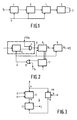
- the reference numeral 1 denotes a staircase voltage generator.
- the staircase-shaped voltage generated thereby is applied to a power amplifier 2 which converts this voltage into a current.
- a field deflection coil 3 through which the said current, the field deflection current flows is connected to an output of amplifier 2.
- Amplifier 2 is formed in known manner as a linear amplifier, particularly due to the use of negative feedback. Consequently the field deflection current would have a shape which is substantially equal to the staricase-shaped output signal of generator 1.
- the voltage of generator 1 may be considered as an essentially sawtooth-shaped voltage.
- generator 1 receives clock pulses which are generated by a clock pulse generator 4.
- the number of clock pulses applied to generator 1 is maintained at a given value by a pulse reduction circuit 5 in a manner to be explained hereinafter.
- the output of circuit 5 is connected to the input of generator 1.
- Line pulses of the signal presented to the picture display device of which the circuit of Fig. 1 forms part are applied to generator 4 for synchronising the clock pulses.
- Field pulses R are applied to generator 4, circuit 5 and generator 1 for their resetting.
- the said line and field pulses may be the pulses which are present in the incoming signal and which are obtained by means of a synchronising signal separator of known type.
- the said pulses may originate from a line or field synchronising circuit with which interference-free signals are obtained in known manner which are substantially synchronous with the corresponding incoming signals.
- Each clock pulse applied to generator 1 causes a given variation of the signal of the generator and there is no variation in the time interval between two successive clock pulses.
- the desired staircase-shaped signal is produced in this manner.
- the field pulse causes a variation in the opposite direction so that the signal level assumes substantially the same value as at the occurrence of the previous field pulse.
- Generator 1 is adapted in such a manner that the variation caused upon the occurrence of each clock pulse has a constant value. In this way the amplitude of the generated staircase is only dependent on the number of clock pulses per field period.
- Generator 1 comprises, for example a capacitor each time receiving a constant charge so that the voltage across the capacitor increases, which capacitor is subsequently discharged by the field pulse.
- the amplitude of the staircase and consequently the height of the picture shown on a display screen is not constant. This is very undesirable.
- a constant number of clock pulses per field period could be obtained by coupling the clock pulse frequency with the field frequency.
- the field frequency may have different values, for example, 50 Hz according to the European television broadcasting standard or 60 Hz in the U.S.A.
- the clock pulse frequency should thus have to be switchable under the influence of a field frequency detection circuit.
- the clock pulse generator should be incorporated in a control loop for controlling the frequency of the generator in dependence upon a detected difference between the incoming field frequency and a frequency which would be derived from that of the generator. In view of the low value of the field frequency such a control would be very impractical.
- the clock pulse frequency in the circuit of Fig. 1 is derived from and synchronized with the incoming line frequency f H and may therefore have difference values.
- f H is, for example 15.750 kHz for the American standard, 15.625 kHz for the European standard and 31.250 kHz for a high-resolution system with 1250 lines per picture and a field frequency of 50 Hz.
- the clock pulses of generator 4 may have the line frequency or a lower frequency.
- a higher frequency which is an integral multiple of the line frequency will preferably be chosen for obtaining a staircase approximating the sawtooth shape as much as possible.
- a frequency is chosen which is 12 times higher than frequency f H and which is derived from the teletext clock present in the picture display device.
- circuit 5 suppresses the superfluous clock pulses.
- the remaining clock pulses are transferred to generator 1.
- a condition is that the number m should be smaller than the lowest line number to be expected, multiplied by 12.
- the pulse reduction circuit 5 may be formed such that all incoming clock pulses are passed on until the number m is reached, whereafter no clock pulse is passed any longer until the next field pulse occurs. The desired amplitude is then reached after the m passed clock pulse, whereafter the level of the signal generated by generator 1 remains unchanged until the end of the field period. In most cases, however, such a signal cannot be used for the field deflection. For this reason the clock pulses suppressed by circuit 5, i.e. 1 out of 5 in the first case considered, 1 out of 21 in the second case and 3 out of 5 clock pulses in the third case are distributed over the entire field period as regularly as possible.
- the signal of generator 1 has a staircase shape with m vertical steps and occasionally with a horizontally extended step. If there is a switch-over after reception of a signal with a given field period, to a signal with a different field period, the m steps are now distributed over a different duration than beforehand so that the sawtooth has a different slope. This is obtained substantially without any time delay.
- the said frequencies are so high that the perturbations have little influence on the operation of amplifier 2 and on the field deflection current.
- a maximum possible value of h and hence of the clock pulse frequency and a minimum possible value of m are important. The figures found will be slightly less favourable if the above-assumed regularity is not exactly achieved.
- the field period has always been referred to, that is to say, no allowance has been made for the fact that the generated essentially sawtooth-shaped signal has a retrace which is not infinitely short. It is therefore more correct to use the term field trace period, i.e. the period of approximately 19 ms for the European standard which is required for vertical visible scanning of the display screen. This means that the constant number m of steps is distributed over the field trace period.
- a clock pulse frequency which is an integral multiple of the line frequency.
- the chrominance sub-carrier frequency which is a non-integral multiple of the line frequency or a frequency derived therefrom, may be chosen alternatively. Since the number m of the clock pulses actually contributing to the sawtooth generation is constant, the number h and hence the clock pulse frequency do not even have to be constant. The only condition imposed on this frequency is that a possible variation thereof, for example as a result of noise, temperature effects or video recorder tape stretch does not give rise to an impermissible variation of the amplitude of the generated sawtooth.
- Fig. 2 shows an embodiment of pulse generator 4.
- a flip-flop 6 receives a pulse originating from the field synchronising circuit and occurring a certain time, for example 12.5 line periods after the commencement of the field period. This pulse indicates the commencement of the field trace period.
- Flip-flop 6 is reset at the end of the field period.
- a pulse whose duration corresponds to that of the field trace and which is applied to an AND gate 7 for keeping this gate open is present at an output of flip-flop 6.
- Clock pulses whose repetition frequency is 12 times the line frequency f H and which originate from the line synchronising circuit are also applied to gate 7.
- the output signal of gate 7 is also the output signal of generator 4. It comprises the clock pulses occurring during the field trace period.
- clock pulses are counted by a 13-bit counter 8 for circuit 5.
- Counter 8 is reset at the end of the field period whilst the content of the counter is taken over by a latch 9. If the content of counter 8 does not change, the number available at the output of latch 9 does not change either, i.e. the number h expressing how many clock pulses have occurred during the field trace period.
- the generator of Fig. 2 has an OR gate 10 and a multiplex circuit 11.
- a field pulse originating from the field synchronising circuit and occurring at the commencement of the field retrace period is applied to an input of gate 10.
- the output signal of circuit 11 is present at another input of gate 10.
- the outputs of counter 8 with the two most significant bits are connected to two inputs of the circuit 11 in which a choice is made between these two bits by means of a signal which originates from the control section of the picture display device and which indicates the value of the line frequency.
- frequency f H has the value of 31.250 kHz (high resolution system)
- the most significant bit of counter 8 is applied by means of circuit 11 to gate 10 for resetting flip - flop 6 and counter 8.
- the number of clock pulses that has to be suppressed by the pulse reduction circuit 5 is known in advance.
- Circuit 5 may thus be designed for regularly suppressing the superfluous pulses, i.e. every sixth pulse in the example of the European television broadcasting standard. If the display systems are not known in advance and if the circuit of Fig. 1 is to be universal circuit 5 must be capable of realising a distribution of the suppressed pulses which is as regular as possible, irrespective of the number h.
- the comparison is effected by means of this stage in such a manner that the sequence of significance of the number present at the outputs of counter 12 is reversed.
- the number whose reversal is larger than the number w give rise to an output signal of stage 13 to be applied to sawtooth generator 1. A series of pulses with a certain regularity is obtained thereby.
- Such a reversal is known per se, namely from United States Patent 3,836,908. The result of this method is, however, not ideal. This will be apparent from a numerical example in which for the sake of simplicity h is chosen to be 31 and m is chosen to be 5.
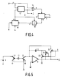
- a more regular distribution is obtained with the circuit of Fig. 4.
- the number h determined by generator 4 is applied to a first input of a comparison stage 15 and via a reversal to an input of an AND-gate 16 another input of which is connected to an output of stage 15.
- An output of gate 16 is connected to an input of a multiplex circuit 17.
- the chosen number m is present in digital form at another input of circuit 17.
- the information chosen is applied to an input of an adder stage 18.
- Another input information of stage 18 is the information of a latch 19 which is also applied to a second input of stage 15.
- the output information of gate 18 is applied to the latch 19 which also receives the clock pulse signal of generator 4.
- the output signal of stage 15 is also the output signal of the circuit of Fig. 4 and it is applied to generator 1.
- circuit 17 passes nothing in the first half of a period of the clock signal and it passes the number m in the second half. At the start of a new clock period the content of latch 19 is equal to the previous content n plus the number m. The same cycle is performed several successive times in which the value of the number n is each time increased, more specifically until n has become equal to or larger than the number h. A logic 1 is then present at the output of stage 15, that is to say, a clock pulse is applied to generator 1, while gate 16 is opened so that the number -h is passed on to circuit 17.
- circuits of Figs. 3 and 4 are examples of circuits for generating pulses with almost equal intervals in between under the influence of binary codes. Such circuits are known under the name of rate multipliers and are described in the literature for interpolative digital-to-analog conversion, for example in the American publication "IEEE Transactions on Communications", Vol. COM-22, No. 11, November 1974, pages 1797 to 1806. An example of such a circuit is also described in "Philips Data Handbook, Electronic components and materials, Integrated circuits, Book ICO4", 1986, pages 539 to 546, type number HEF4527B. It is apparent from Fig. 4 on page 545 that a number of pulses preprogrammed from a given number of pulses is passed on.
- This circuit is used for arithmetic operations. It will be evident that a choice may be made from these circuits for use as a pulse reduction circuit in the field deflection circuit according to the invention.
- the circuit described with reference to Fig. 4 is preferred in view of the more regular distribution of the output pulses.
- the components 8 and 9 operate as analog-to-digital converters, namely for converting the analog pulses at the output of gate 7 into the digital number h which is applied to the pulse reduction circuit 5. It will thus be evident that other known analog-to-digital converters can be used for the same purpose.
- Fig. 5 shows a preferred embodiment of this generator which is a circuit with switched capacitors.
- the circuit comprises two capacitors C1 of approximately 0.1 pF and C2 of approximately 200 pF which are both integrated in a semiconductor body comprising all components of the deflection circuits of Fig. 1 with the exception of capacitors having a large capacitance and possibly elements having a large dissipation in circuit 2, and with the exception of coil 3.
- connection of capacitor C1 shown on the left may be connected via a switch S1 either to a DC voltage source V or to ground, and the connection of the capacitor shown on the right can be connected either to ground or to an inverting input terminal of an amplifier A a non-inverting input terminal of which is connected to ground.
- a connection of capacitor C2 is connected to the said inverting input terminal.
- the other connection of the capacitor may be connected to an output terminal of amplifier A via a switch S4 and to ground via a switch S5.
- a switch S3 is arranged between the inverting input terminal and the output terminal of amplifier A.
- Switches S1 and S2 are operated by the clock pulses from circuit 5. During the first half of a clock period, in which period capacitor C1 is connected to source V at one end and to ground at the other end, capacitor C1 is charged under the voltage of source V and during the second half of the period, in which switches S1 and S2 are in the other position, capacitor C1 is discharged whilst the charge stored therein is transferred to capacitor C2. For this purpose switch S4 conducts while switches S3 and S5 are blocked. In this way an essentially linearly varying voltage with a decreasing variation is produced at the output of amplifier A.
- switches S3, S4 and S5 are changed over under the influence of the field reset pulse R from gate 10 and this in such a manner that switches S3 and S5 conduct while switch S4 is blocked.
- Capacitor C2 is discharged by the output of amplifier A. Thanks to switches S3 and S4 an offset voltage which may be present at the output terminal of amplifier A has no influence on the level of the essentially sawtooth-shaped voltage produced, which level is assumed at the end of discharging capacitor C2. This level is determined by the potential with which switch S5 is connected, i.e. that of ground in the embodiment of Fig. 5.
- V is the value of the voltage of the source V.
- the output of amplifier A or the connection of capacitor C2 shown on the right is connected to the power amplifier 2.
Landscapes
- Engineering & Computer Science (AREA)
- Multimedia (AREA)
- Signal Processing (AREA)
- Power Engineering (AREA)
- Details Of Television Scanning (AREA)
Claims (7)
- Vertikal-Ablenkschaltung in einer Bildwiedergabeanordnung zum Empfangen und Verarbeiten eines Signals mit Zeilen- und Teilbildimpulsen, wobei diese Vertikal-Ablenkschaltung einen Taktimpulsgenerator (4), einen Sägezahngenerator (1), einen mit dem Sägezahngenerator (1) gekoppelten Leistungsverstärker (2) sowie eine mit dem Leistungsverstärker (2) gekoppelte Vertikal-Ablenkspule (3) aufweist, wobei der Sägezahngenerator (1) mit einem Speicherelement zum Speichern von Information unter dem Einfluß zugeführter Taktimpulse, sowie mit Rückstellmitteln versehen ist zum Rückstellen des Speicherelementes unter dem Einfluß der Teilbildimpulse, dadurch gekennzeichnet, daß die Vertikal-Ablenkschaltung ebenfalls eine mit dem Taktimpulsgenerator (4) gekoppelte Impulsverringerungsschaltung (5) aufweist, welche die je Vertikal-Periode dem Sägezahngenerator (1) zugeführte, von dem Taktimpulsgenerator (4) erzeugte Anzahl Taktimpulse auf eine vorbestimmte Anzahl m verringert.
- Vertikal-Ablenkschaltung nach Anspruch 1, dadurch gekennzeichnet, daß die Impulsverringerungsschaltung (5) mit einem Geschwindigkeitsmultiplizierer versehen ist zur nahezu regelmäßigen Verteilung der während der Vertikal-Periode dem Sägezahngenerator (1) zugeführten Taktimpulse.
- Vertikal-Ablenkschaltung nach Anspruch 2, dadurch gekennzeichnet, daß die Impulsverringerungsschaltung (5) einen Zähler (8) aufweist, der zur Bestimmung der Anzahl je Vertikal-Periode erzeugter Taktimpulse h mit dem Taktimpulsgenerator (4) verbunden ist, sowie eine mit dem Zähler verbundene Verriegelungsschaltung (9) zur Speicherung der Anzahl h während nur einer Vertikal-Periode, wobei diese Anzahl festgestellt wird durch den Zähler (8) der vom Taktimpulsgenerator (4) je Vertikal-Periode erzeugten Taktimpulse, und daß der Geschwindigkeitsmultiplizierer einen mit der Verriegelungsschaltung (9) verbundenen Rückwärtszähler (12) aufweist zum Zählen von der Zahl h zu Null, sowie eine Subtrahierstufe (14) zum Subtrahieren der vorbestimmten Zahl m von der Zahl h, und eine Vergleichsstufe (13) zum Vergleichen des Ergebnisses der Subtraktion mit der Zählung des Rückwärtszählers (12), deren Signifikanz umgekehrt wird, wobei die Vergleichsstufe (13) dem Sägezahngenerator (1) Taktimpulse zuführt, wenn die umgekehrte Zählung größer ist als das Subtraktionsergebnis.
- Vertikal-Ablenkschaltung nach Anspruch 2, dadurch gekennzeichnet, daß die Impulsverringerungsschaltung (5) einen Zähler (8) aufweist, der mit dem Taktimpulsgenerator (4) verbunden ist zum Bestimmen der Anzahl je Vertikal-Periode erzeugter Taktimpulse h und eine mit dem Zähler (8) verbundene Verriegelungsschaltung (9) zur Speicherung der Anzahl h während nur einer Vertikal-Periode, wobei diese Anzahl festgestellt wird durch den Zähler (8) der vom Taktimpulsgenerator (4) je Vertikal-Periode erzeugten Taktimpulse, und daß der Geschwindigkeitsmultiplizierer eine mit der Verriegelungsstufe (9) verbundene Vergleichsstufe (15) aufweist, zum Vergleichen der Anzahl h mit einem Inhalt n eines Speichers (19), der die vom Taktimpulsgenerator (4) erzeugten Taktimpulse erhält, wobei nach einer Taktimpulsperiode der genannte Inhalt


- Vertikal-Ablenkschaltung nach Anspruch 1, dadurch gekennzeichnet, daß diese Schaltungsanordnung einen mit dem Taktimpulsgenerator (4) verbundenen Zähler (8) aufweist zum Bestimmen der Anzahl je Vertikal-Periode erzeugter Taktimpulse h, sowie ein Gatter (10) zum Hindurchlassen eines von dem Zähler (8) erzeugten Impulses zum Rückstellen des Taktimpulsgenerators (4) und des Sägezahngenerators (1) beim Fehlen eines erhaltenen Teilbildimpulses, wobei das Auftreten des erzeugten Teilbildimpulses einer Frequenz entspricht, die niedriger ist als die niedrigste Vertikal-Frequenz in dem Signal, für das die Bildwiedergabeanordnung geeignet ist.
- Vertikal-Ablenkschaltung nach Anspruch 5, dadurch gekennzeichnet, daß der von dem Zähler (8) erzeugte Impuls ebenfalls der Rückstellimpuls für das Speicherelement ist.
- Vertikal-Ablenkschaltung nach einem der vorstehenden Ansprüche, dadurch gekennzeichnet, daß die Frequenz der Taktimpulse ein ganzes Vielfaches der Horizontal-Frequenz ist.
Applications Claiming Priority (2)
| Application Number | Priority Date | Filing Date | Title |
|---|---|---|---|
| NL8701692 | 1987-07-17 | ||
| NL8701692 | 1987-07-17 |
Publications (2)
| Publication Number | Publication Date |
|---|---|
| EP0301633A1 EP0301633A1 (de) | 1989-02-01 |
| EP0301633B1 true EP0301633B1 (de) | 1993-03-31 |
Family
ID=19850334
Family Applications (1)
| Application Number | Title | Priority Date | Filing Date |
|---|---|---|---|
| EP88201482A Expired - Lifetime EP0301633B1 (de) | 1987-07-17 | 1988-07-12 | Vertikal-Ablenkschaltung in einer Bildwiedergabeanordnung |
Country Status (6)
| Country | Link |
|---|---|
| US (1) | US4891565A (de) |
| EP (1) | EP0301633B1 (de) |
| JP (1) | JPS6441379A (de) |
| KR (1) | KR890003199A (de) |
| DE (1) | DE3879797T2 (de) |
| FI (1) | FI87503C (de) |
Families Citing this family (3)
| Publication number | Priority date | Publication date | Assignee | Title |
|---|---|---|---|---|
| NL8901147A (nl) * | 1989-05-08 | 1990-12-03 | Philips Nv | Schakeling voor het leveren van een periodiek in wezen paraboolvormig signaal. |
| US5343301A (en) * | 1992-11-05 | 1994-08-30 | Ampex Systems Corporation | Input clock presence detector for a digital video input |
| WO2001082483A1 (en) * | 2000-04-26 | 2001-11-01 | Koninklijke Philips Electronics N.V. | Apparatus and method for generating a periodic non-linear waveform |
Family Cites Families (6)
| Publication number | Priority date | Publication date | Assignee | Title |
|---|---|---|---|---|
| US3758825A (en) * | 1971-08-20 | 1973-09-11 | Bel Tel Lab Inc | Digital deflection system for cathode ray tubes |
| DE2317851B2 (de) * | 1973-04-10 | 1975-04-24 | Grundig E.M.V. Elektro-Mechanische Versuchsanstalt Max Grundig, 8510 Fuerth | Digital-Analog-Wandler |
| US4228461A (en) * | 1979-05-25 | 1980-10-14 | Zenith Radio Corporation | Vertical synchronization system |
| US4334174A (en) * | 1979-09-21 | 1982-06-08 | Zenith Radio Corporation | Sawtooth waveform generation for a television receiver |
| US4361785A (en) * | 1979-10-01 | 1982-11-30 | K&R Engineering Sales Corporation | Versatile video CRT display |
| GB2095491A (en) * | 1981-03-02 | 1982-09-29 | Croma Research Ltd | Constant amplitude sawtooth generator |
-
1988
- 1988-06-24 US US07/211,306 patent/US4891565A/en not_active Expired - Fee Related
- 1988-07-12 DE DE88201482T patent/DE3879797T2/de not_active Expired - Fee Related
- 1988-07-12 EP EP88201482A patent/EP0301633B1/de not_active Expired - Lifetime
- 1988-07-14 KR KR1019880008726A patent/KR890003199A/ko not_active Withdrawn
- 1988-07-14 FI FI883353A patent/FI87503C/fi not_active IP Right Cessation
- 1988-07-16 JP JP63176252A patent/JPS6441379A/ja active Pending
Also Published As
| Publication number | Publication date |
|---|---|
| FI883353A0 (fi) | 1988-07-14 |
| DE3879797D1 (de) | 1993-05-06 |
| KR890003199A (ko) | 1989-04-13 |
| JPS6441379A (en) | 1989-02-13 |
| FI883353L (fi) | 1989-01-18 |
| FI87503B (fi) | 1992-09-30 |
| DE3879797T2 (de) | 1993-09-30 |
| FI87503C (fi) | 1993-01-11 |
| EP0301633A1 (de) | 1989-02-01 |
| US4891565A (en) | 1990-01-02 |
Similar Documents
| Publication | Publication Date | Title |
|---|---|---|
| US4292654A (en) | Deflection system and switched-mode power supply using a common ramp generator | |
| US4351002A (en) | Circuit for correcting phase deviations between the line deflection drive signals and the line synchronizing signals in a television receiver | |
| US5043813A (en) | Display locked timing signals for video processing | |
| US4891565A (en) | Field deflection circuit in a picture display device | |
| US4827343A (en) | Method and apparatus for reducing analog/digital converter requirements in picture-in-picture television circuits | |
| FI71049C (fi) | Horisontalsynkroniseringsarrangemang foer en televisionanvisningsapparat | |
| US4336513A (en) | Hum reduction circuit | |
| US4024343A (en) | Circuit arrangement for synchronizing an output signal in accordance with a periodic pulsatory input signal | |
| EP0397239B1 (de) | Schaltungsanordnung zum Liefern eines periodischen, im wesentlichen parabelförmigen Signals | |
| US4833371A (en) | Picture display device with symmetrical deflection | |
| EP0423882B1 (de) | Schaltungsanordnung in einer Bildwiedergabeanordnung mit einer Videosignalverarbeitungsschaltung und einer Zeilensynchronschaltung | |
| EP0265986B1 (de) | Vertikal-Ablenkschaltung in einer Bildwiedergabevorrichtung | |
| JP2539784B2 (ja) | 画像処理システム | |
| EP0314219B1 (de) | Horizontal-Synchronschaltung | |
| US5003392A (en) | Circuit for digitally deriving pulses of horizontal and vertical frequency from a synchronizing signal | |
| FI104775B (fi) | Tahdistettu vaakapyyhkäisy vaakataajuuden monikerroilla | |
| EP0963075A2 (de) | Taktsignalerzeugungsvorrichtung | |
| EP0322743B1 (de) | Signalgenerator | |
| EP0406949B1 (de) | Oszillatorschaltung | |
| EP0289082A1 (de) | Digital-Analog-Wandler | |
| EP0287168A1 (de) | Bildwiedergabevorrichtung mit einer Schaltung zur Umwandlung der Anzahl von Teilbildern | |
| WO1998043439A9 (en) | Video synchronizing signal generator | |
| JPH01238694A (ja) | 画像表示装置 | |
| JPH07239385A (ja) | 放射線量測定装置 | |
| US5376906A (en) | CCD filter having comb-shaped characteristics |
Legal Events
| Date | Code | Title | Description |
|---|---|---|---|
| PUAI | Public reference made under article 153(3) epc to a published international application that has entered the european phase |
Free format text: ORIGINAL CODE: 0009012 |
|
| AK | Designated contracting states |
Kind code of ref document: A1 Designated state(s): BE DE FR GB IT NL |
|
| 17P | Request for examination filed |
Effective date: 19890715 |
|
| 17Q | First examination report despatched |
Effective date: 19900903 |
|
| GRAA | (expected) grant |
Free format text: ORIGINAL CODE: 0009210 |
|
| AK | Designated contracting states |
Kind code of ref document: B1 Designated state(s): BE DE FR GB IT NL |
|
| PG25 | Lapsed in a contracting state [announced via postgrant information from national office to epo] |
Ref country code: NL Effective date: 19930331 Ref country code: BE Effective date: 19930331 |
|
| REF | Corresponds to: |
Ref document number: 3879797 Country of ref document: DE Date of ref document: 19930506 |
|
| ITF | It: translation for a ep patent filed | ||
| ET | Fr: translation filed | ||
| NLV1 | Nl: lapsed or annulled due to failure to fulfill the requirements of art. 29p and 29m of the patents act | ||
| PLBE | No opposition filed within time limit |
Free format text: ORIGINAL CODE: 0009261 |
|
| STAA | Information on the status of an ep patent application or granted ep patent |
Free format text: STATUS: NO OPPOSITION FILED WITHIN TIME LIMIT |
|
| 26N | No opposition filed | ||
| ITPR | It: changes in ownership of a european patent |
Owner name: CAMBIO RAGIONE SOCIALE;PHILIPS ELECTRONICS N.V. |
|
| REG | Reference to a national code |
Ref country code: FR Ref legal event code: CD |
|
| PGFP | Annual fee paid to national office [announced via postgrant information from national office to epo] |
Ref country code: GB Payment date: 19980701 Year of fee payment: 11 |
|
| PGFP | Annual fee paid to national office [announced via postgrant information from national office to epo] |
Ref country code: FR Payment date: 19980716 Year of fee payment: 11 |
|
| REG | Reference to a national code |
Ref country code: FR Ref legal event code: CD |
|
| PGFP | Annual fee paid to national office [announced via postgrant information from national office to epo] |
Ref country code: DE Payment date: 19980925 Year of fee payment: 11 |
|
| PG25 | Lapsed in a contracting state [announced via postgrant information from national office to epo] |
Ref country code: GB Free format text: LAPSE BECAUSE OF NON-PAYMENT OF DUE FEES Effective date: 19990712 |
|
| PG25 | Lapsed in a contracting state [announced via postgrant information from national office to epo] |
Ref country code: FR Free format text: THE PATENT HAS BEEN ANNULLED BY A DECISION OF A NATIONAL AUTHORITY Effective date: 19990731 |
|
| GBPC | Gb: european patent ceased through non-payment of renewal fee |
Effective date: 19990712 |
|
| PG25 | Lapsed in a contracting state [announced via postgrant information from national office to epo] |
Ref country code: DE Free format text: LAPSE BECAUSE OF NON-PAYMENT OF DUE FEES Effective date: 20000503 |
|
| REG | Reference to a national code |
Ref country code: FR Ref legal event code: ST |
|
| PG25 | Lapsed in a contracting state [announced via postgrant information from national office to epo] |
Ref country code: IT Free format text: LAPSE BECAUSE OF NON-PAYMENT OF DUE FEES;WARNING: LAPSES OF ITALIAN PATENTS WITH EFFECTIVE DATE BEFORE 2007 MAY HAVE OCCURRED AT ANY TIME BEFORE 2007. THE CORRECT EFFECTIVE DATE MAY BE DIFFERENT FROM THE ONE RECORDED. Effective date: 20050712 |