EP0299752B1 - Kontrolle eines Verfahrens zur Abscheidung eines dünnen Filmes mittels Plasma - Google Patents
Kontrolle eines Verfahrens zur Abscheidung eines dünnen Filmes mittels Plasma Download PDFInfo
- Publication number
- EP0299752B1 EP0299752B1 EP88306431A EP88306431A EP0299752B1 EP 0299752 B1 EP0299752 B1 EP 0299752B1 EP 88306431 A EP88306431 A EP 88306431A EP 88306431 A EP88306431 A EP 88306431A EP 0299752 B1 EP0299752 B1 EP 0299752B1
- Authority
- EP
- European Patent Office
- Prior art keywords
- plasma
- ratio
- emission
- intensity
- species
- Prior art date
- Legal status (The legal status is an assumption and is not a legal conclusion. Google has not performed a legal analysis and makes no representation as to the accuracy of the status listed.)
- Expired - Lifetime
Links
- 238000000427 thin-film deposition Methods 0.000 title description 5
- 238000004886 process control Methods 0.000 title description 4
- 238000000034 method Methods 0.000 claims abstract description 71
- 230000008569 process Effects 0.000 claims abstract description 47
- 239000000758 substrate Substances 0.000 claims abstract description 32
- 238000000151 deposition Methods 0.000 claims abstract description 21
- 239000010409 thin film Substances 0.000 claims abstract description 21
- 239000007789 gas Substances 0.000 claims description 53
- QVGXLLKOCUKJST-UHFFFAOYSA-N atomic oxygen Chemical compound [O] QVGXLLKOCUKJST-UHFFFAOYSA-N 0.000 claims description 13
- 239000001301 oxygen Substances 0.000 claims description 13
- 229910052760 oxygen Inorganic materials 0.000 claims description 13
- 239000000463 material Substances 0.000 claims description 9
- 230000005684 electric field Effects 0.000 claims description 8
- 230000005670 electromagnetic radiation Effects 0.000 claims description 7
- 238000005137 deposition process Methods 0.000 claims description 5
- 239000011261 inert gas Substances 0.000 claims description 4
- 230000005855 radiation Effects 0.000 claims description 4
- 230000001419 dependent effect Effects 0.000 claims description 2
- 239000010408 film Substances 0.000 abstract description 25
- 230000003287 optical effect Effects 0.000 abstract description 8
- 239000001257 hydrogen Substances 0.000 description 30
- 229910052739 hydrogen Inorganic materials 0.000 description 30
- UFHFLCQGNIYNRP-UHFFFAOYSA-N Hydrogen Chemical compound [H][H] UFHFLCQGNIYNRP-UHFFFAOYSA-N 0.000 description 29
- 238000006243 chemical reaction Methods 0.000 description 18
- 229910052734 helium Inorganic materials 0.000 description 17
- SWQJXJOGLNCZEY-UHFFFAOYSA-N helium atom Chemical compound [He] SWQJXJOGLNCZEY-UHFFFAOYSA-N 0.000 description 17
- 239000001307 helium Substances 0.000 description 16
- 230000008021 deposition Effects 0.000 description 14
- 238000012545 processing Methods 0.000 description 13
- 238000009792 diffusion process Methods 0.000 description 12
- XUIMIQQOPSSXEZ-UHFFFAOYSA-N Silicon Chemical compound [Si] XUIMIQQOPSSXEZ-UHFFFAOYSA-N 0.000 description 10
- 229910052710 silicon Inorganic materials 0.000 description 10
- 238000005334 plasma enhanced chemical vapour deposition Methods 0.000 description 9
- 238000000623 plasma-assisted chemical vapour deposition Methods 0.000 description 9
- 239000010703 silicon Substances 0.000 description 9
- 239000013307 optical fiber Substances 0.000 description 8
- 230000008859 change Effects 0.000 description 7
- 238000000576 coating method Methods 0.000 description 7
- 238000012544 monitoring process Methods 0.000 description 7
- 239000011248 coating agent Substances 0.000 description 6
- 230000007423 decrease Effects 0.000 description 6
- 238000001228 spectrum Methods 0.000 description 6
- 230000008901 benefit Effects 0.000 description 5
- 238000004364 calculation method Methods 0.000 description 5
- 238000010586 diagram Methods 0.000 description 5
- 238000004544 sputter deposition Methods 0.000 description 5
- 238000000295 emission spectrum Methods 0.000 description 4
- 239000011521 glass Substances 0.000 description 4
- 230000004044 response Effects 0.000 description 4
- OKTJSMMVPCPJKN-UHFFFAOYSA-N Carbon Chemical group [C] OKTJSMMVPCPJKN-UHFFFAOYSA-N 0.000 description 3
- 239000000835 fiber Substances 0.000 description 3
- 238000002955 isolation Methods 0.000 description 3
- 238000005259 measurement Methods 0.000 description 3
- 230000007246 mechanism Effects 0.000 description 3
- 238000005086 pumping Methods 0.000 description 3
- 239000010453 quartz Substances 0.000 description 3
- 239000000523 sample Substances 0.000 description 3
- VYPSYNLAJGMNEJ-UHFFFAOYSA-N silicon dioxide Inorganic materials O=[Si]=O VYPSYNLAJGMNEJ-UHFFFAOYSA-N 0.000 description 3
- 238000012360 testing method Methods 0.000 description 3
- XKRFYHLGVUSROY-UHFFFAOYSA-N Argon Chemical compound [Ar] XKRFYHLGVUSROY-UHFFFAOYSA-N 0.000 description 2
- 229910002808 Si–O–Si Inorganic materials 0.000 description 2
- RTAQQCXQSZGOHL-UHFFFAOYSA-N Titanium Chemical compound [Ti] RTAQQCXQSZGOHL-UHFFFAOYSA-N 0.000 description 2
- 125000004429 atom Chemical group 0.000 description 2
- 238000004422 calculation algorithm Methods 0.000 description 2
- 229910052799 carbon Inorganic materials 0.000 description 2
- 238000004590 computer program Methods 0.000 description 2
- 230000000694 effects Effects 0.000 description 2
- 230000005284 excitation Effects 0.000 description 2
- UQEAIHBTYFGYIE-UHFFFAOYSA-N hexamethyldisiloxane Chemical compound C[Si](C)(C)O[Si](C)(C)C UQEAIHBTYFGYIE-UHFFFAOYSA-N 0.000 description 2
- 125000004435 hydrogen atom Chemical group [H]* 0.000 description 2
- 239000007788 liquid Substances 0.000 description 2
- 125000002496 methyl group Chemical group [H]C([H])([H])* 0.000 description 2
- 239000000203 mixture Substances 0.000 description 2
- 239000010936 titanium Substances 0.000 description 2
- 229910052719 titanium Inorganic materials 0.000 description 2
- YZCKVEUIGOORGS-UHFFFAOYSA-N Hydrogen atom Chemical compound [H] YZCKVEUIGOORGS-UHFFFAOYSA-N 0.000 description 1
- 229910018540 Si C Inorganic materials 0.000 description 1
- 229910018557 Si O Inorganic materials 0.000 description 1
- NRTOMJZYCJJWKI-UHFFFAOYSA-N Titanium nitride Chemical compound [Ti]#N NRTOMJZYCJJWKI-UHFFFAOYSA-N 0.000 description 1
- 239000004411 aluminium Substances 0.000 description 1
- 229910052782 aluminium Inorganic materials 0.000 description 1
- XAGFODPZIPBFFR-UHFFFAOYSA-N aluminium Chemical compound [Al] XAGFODPZIPBFFR-UHFFFAOYSA-N 0.000 description 1
- 239000005328 architectural glass Substances 0.000 description 1
- 229910052786 argon Inorganic materials 0.000 description 1
- 230000009286 beneficial effect Effects 0.000 description 1
- 230000005540 biological transmission Effects 0.000 description 1
- 229910021386 carbon form Inorganic materials 0.000 description 1
- 150000001875 compounds Chemical class 0.000 description 1
- 239000000470 constituent Substances 0.000 description 1
- 230000008878 coupling Effects 0.000 description 1
- 238000010168 coupling process Methods 0.000 description 1
- 238000005859 coupling reaction Methods 0.000 description 1
- 238000004132 cross linking Methods 0.000 description 1
- 230000000593 degrading effect Effects 0.000 description 1
- 238000001739 density measurement Methods 0.000 description 1
- 230000005281 excited state Effects 0.000 description 1
- 238000009501 film coating Methods 0.000 description 1
- 239000003574 free electron Substances 0.000 description 1
- 239000008246 gaseous mixture Substances 0.000 description 1
- 230000009191 jumping Effects 0.000 description 1
- 239000011344 liquid material Substances 0.000 description 1
- 229910052751 metal Inorganic materials 0.000 description 1
- 239000002184 metal Substances 0.000 description 1
- 125000004430 oxygen atom Chemical group O* 0.000 description 1
- 230000000737 periodic effect Effects 0.000 description 1
- 230000035699 permeability Effects 0.000 description 1
- 239000004033 plastic Substances 0.000 description 1
- 229920003023 plastic Polymers 0.000 description 1
- 239000000376 reactant Substances 0.000 description 1
- 230000003678 scratch resistant effect Effects 0.000 description 1
- 238000006748 scratching Methods 0.000 description 1
- 230000002393 scratching effect Effects 0.000 description 1
- 229910010271 silicon carbide Inorganic materials 0.000 description 1
- LIVNPJMFVYWSIS-UHFFFAOYSA-N silicon monoxide Inorganic materials [Si-]#[O+] LIVNPJMFVYWSIS-UHFFFAOYSA-N 0.000 description 1
- 239000002210 silicon-based material Substances 0.000 description 1
- 239000007787 solid Substances 0.000 description 1
- 125000006850 spacer group Chemical group 0.000 description 1
- 230000004304 visual acuity Effects 0.000 description 1
Images




Classifications
-
- C—CHEMISTRY; METALLURGY
- C08—ORGANIC MACROMOLECULAR COMPOUNDS; THEIR PREPARATION OR CHEMICAL WORKING-UP; COMPOSITIONS BASED THEREON
- C08J—WORKING-UP; GENERAL PROCESSES OF COMPOUNDING; AFTER-TREATMENT NOT COVERED BY SUBCLASSES C08B, C08C, C08F, C08G or C08H
- C08J5/00—Manufacture of articles or shaped materials containing macromolecular substances
- C08J5/12—Bonding of a preformed macromolecular material to the same or other solid material such as metal, glass, leather, e.g. using adhesives
-
- C—CHEMISTRY; METALLURGY
- C23—COATING METALLIC MATERIAL; COATING MATERIAL WITH METALLIC MATERIAL; CHEMICAL SURFACE TREATMENT; DIFFUSION TREATMENT OF METALLIC MATERIAL; COATING BY VACUUM EVAPORATION, BY SPUTTERING, BY ION IMPLANTATION OR BY CHEMICAL VAPOUR DEPOSITION, IN GENERAL; INHIBITING CORROSION OF METALLIC MATERIAL OR INCRUSTATION IN GENERAL
- C23C—COATING METALLIC MATERIAL; COATING MATERIAL WITH METALLIC MATERIAL; SURFACE TREATMENT OF METALLIC MATERIAL BY DIFFUSION INTO THE SURFACE, BY CHEMICAL CONVERSION OR SUBSTITUTION; COATING BY VACUUM EVAPORATION, BY SPUTTERING, BY ION IMPLANTATION OR BY CHEMICAL VAPOUR DEPOSITION, IN GENERAL
- C23C14/00—Coating by vacuum evaporation, by sputtering or by ion implantation of the coating forming material
- C23C14/0021—Reactive sputtering or evaporation
- C23C14/0036—Reactive sputtering
- C23C14/0042—Controlling partial pressure or flow rate of reactive or inert gases with feedback of measurements
-
- C—CHEMISTRY; METALLURGY
- C23—COATING METALLIC MATERIAL; COATING MATERIAL WITH METALLIC MATERIAL; CHEMICAL SURFACE TREATMENT; DIFFUSION TREATMENT OF METALLIC MATERIAL; COATING BY VACUUM EVAPORATION, BY SPUTTERING, BY ION IMPLANTATION OR BY CHEMICAL VAPOUR DEPOSITION, IN GENERAL; INHIBITING CORROSION OF METALLIC MATERIAL OR INCRUSTATION IN GENERAL
- C23C—COATING METALLIC MATERIAL; COATING MATERIAL WITH METALLIC MATERIAL; SURFACE TREATMENT OF METALLIC MATERIAL BY DIFFUSION INTO THE SURFACE, BY CHEMICAL CONVERSION OR SUBSTITUTION; COATING BY VACUUM EVAPORATION, BY SPUTTERING, BY ION IMPLANTATION OR BY CHEMICAL VAPOUR DEPOSITION, IN GENERAL
- C23C14/00—Coating by vacuum evaporation, by sputtering or by ion implantation of the coating forming material
- C23C14/22—Coating by vacuum evaporation, by sputtering or by ion implantation of the coating forming material characterised by the process of coating
- C23C14/54—Controlling or regulating the coating process
-
- C—CHEMISTRY; METALLURGY
- C23—COATING METALLIC MATERIAL; COATING MATERIAL WITH METALLIC MATERIAL; CHEMICAL SURFACE TREATMENT; DIFFUSION TREATMENT OF METALLIC MATERIAL; COATING BY VACUUM EVAPORATION, BY SPUTTERING, BY ION IMPLANTATION OR BY CHEMICAL VAPOUR DEPOSITION, IN GENERAL; INHIBITING CORROSION OF METALLIC MATERIAL OR INCRUSTATION IN GENERAL
- C23C—COATING METALLIC MATERIAL; COATING MATERIAL WITH METALLIC MATERIAL; SURFACE TREATMENT OF METALLIC MATERIAL BY DIFFUSION INTO THE SURFACE, BY CHEMICAL CONVERSION OR SUBSTITUTION; COATING BY VACUUM EVAPORATION, BY SPUTTERING, BY ION IMPLANTATION OR BY CHEMICAL VAPOUR DEPOSITION, IN GENERAL
- C23C16/00—Chemical coating by decomposition of gaseous compounds, without leaving reaction products of surface material in the coating, i.e. chemical vapour deposition [CVD] processes
- C23C16/44—Chemical coating by decomposition of gaseous compounds, without leaving reaction products of surface material in the coating, i.e. chemical vapour deposition [CVD] processes characterised by the method of coating
- C23C16/50—Chemical coating by decomposition of gaseous compounds, without leaving reaction products of surface material in the coating, i.e. chemical vapour deposition [CVD] processes characterised by the method of coating using electric discharges
-
- C—CHEMISTRY; METALLURGY
- C23—COATING METALLIC MATERIAL; COATING MATERIAL WITH METALLIC MATERIAL; CHEMICAL SURFACE TREATMENT; DIFFUSION TREATMENT OF METALLIC MATERIAL; COATING BY VACUUM EVAPORATION, BY SPUTTERING, BY ION IMPLANTATION OR BY CHEMICAL VAPOUR DEPOSITION, IN GENERAL; INHIBITING CORROSION OF METALLIC MATERIAL OR INCRUSTATION IN GENERAL
- C23C—COATING METALLIC MATERIAL; COATING MATERIAL WITH METALLIC MATERIAL; SURFACE TREATMENT OF METALLIC MATERIAL BY DIFFUSION INTO THE SURFACE, BY CHEMICAL CONVERSION OR SUBSTITUTION; COATING BY VACUUM EVAPORATION, BY SPUTTERING, BY ION IMPLANTATION OR BY CHEMICAL VAPOUR DEPOSITION, IN GENERAL
- C23C16/00—Chemical coating by decomposition of gaseous compounds, without leaving reaction products of surface material in the coating, i.e. chemical vapour deposition [CVD] processes
- C23C16/44—Chemical coating by decomposition of gaseous compounds, without leaving reaction products of surface material in the coating, i.e. chemical vapour deposition [CVD] processes characterised by the method of coating
- C23C16/52—Controlling or regulating the coating process
Definitions
- This invention relates generally to plasma diagnostics and process control in depositing thin films on substrates, particularly those processes utilising sputtering, plasma enhanced chemical vapour deposition (PECVD) and plasma polymerisation.
- PECVD plasma enhanced chemical vapour deposition
- a thin film depositing plasma is formed in a chamber by introducing at least one gas into a region of a controlled electrical field.
- Many such plasma processes operate at low pressure with magnetic confinement.
- Most plasma processes involve a control of at least the internal pressure level, the electrical field characteristics, and the composition and proportional flow rates of individual gases into the plasma. Selection of these variables, in turn, affects the properties of a resulting thin film.
- Such properties can include the film's hardness, its adhesion to the substrate, its permeability to certain liquids or gases, optical characteristics of translucence and refractive index, and its general composition.
- the property or properties of the resulting film that are important depend upon the purpose and application of the resulting product.
- the film's hardness, adhesion to glass and degree of optical clarity are the most important properties.
- a coating is desired to prevent the permeation of oxygen, that property of the thin film is most important.
- characteristics of the emission of electromagnetic radiation in the visible and near visible regions of the plasma are monitored, such as by use of a spectrometer, and input variables to the plasma process are controlled in response to this monitoring.
- the purpose of this monitoring and control is to maintain the monitored aspects of the plasma emission at a level that has been determined to relate to certain desired properties of the thin film that is being deposited. Such properties may be resistance to scratching or optical clarity of the film, as examples.
- Certain aspects of the plasma emission found to correlate with a high film deposition rate can also be controlled. These plasma characteristics are controlled in real time by automatically making any adjustments to the plasma input variables that are necessary to maintain the monitored plasma emission characteristics within close limits. This results in the thin film coating being uniform and the process being repeatable. The necessity for independent test depositions and subsequent analysis of the film properties is minimised. A high yield process for commercially coating large substrates is made practical by this diagnostic and control technique.
- the intensity of each of a plurality of lines of emission of the plasma is measured and compared. It has been found that the average electron temperature (T e ) in the plasma is proportional to a ratio of the intensities of two lines of emissions from a single species in the plasma. Since such a species has been excited to emission by adsorbing energy from colliding electrons, the intensity of the lines is proportional to such an average energy. By comparing emission line intensities, the distribution of those energies can be estimated and T e calculated.
- the average electron temperature of the plasma affects the film deposition rate and properties of the resulting film, so it is an important piece of information to have in a real time plasma control system.
- the ratio of intensities of the emission lines in the single species may be controlled directly by adjusting the plasma input variables until a predetermined value of the ratio is obtained, the predetermined value having been earlier determined to provide a film having the desired properties.
- a system is schematically illustrated that includes an enclosed reaction chamber 11 in which a plasma is formed and in which a substrate, such as substrate 13, is placed for depositing a thin film of material on it.
- the substrate 13 can be any vacuum compatible material, such as metal, glass, some plastics and coated substrates.
- One or more gases are supplied to the reaction chamber by a gas supply system 15.
- An electric field is created by a power supply 17, and a low pressure is maintained by a pressure control system 19.
- An optical emission spectrometer 21 is connected through an optical fibre light transmission medium 23 to the reaction chamber in some appropriate manner to couple the visible and near visible emission (especially the ultraviolet wavelengths) of the plasma to the spectrometer.
- a quartz window 24 in a side wall of the reaction chamber can be used to optically couple the plasma emission with the external fibre medium 23.
- a general system control 25, including a computer control portion, is connected to each of the other components of the system in a manner to receive status information from them and send controlling commands to them.
- the reaction chamber 11 can, in the system of Figure 1, be of an appropriate type to perform any of the sputtering, plasma-enhanced chemical vapour deposition (PECVD), plasma polymerisation processes or other vacuum thin film deposition processes.
- PECVD plasma-enhanced chemical vapour deposition
- the reaction chamber 11 is divided into a load lock compartment 27 and a process compartment 29 by an isolation slit valve 31.
- the pressure control system 19 includes a mechanical pump 33 connected to the load lock chamber 27 by a valve 35.
- the pressure control system also includes diffusion pumps 37 and 39, and an associated mechanical pump 41.
- the diffusion pump 37 is connected to the load lock chamber 27 through an isolation gate valve 43 and an adjustable baffle 45.
- the diffusion pump 39 is connected to the process chamber 29 through an isolation gate valve 47 and an adjustable baffle 49.
- the baffle 49 is controlled by the system control 25, while a coating process is being carried out, in order to maintain the internal pressure at a desired value.
- a substrate to be coated is first loaded into the load lock compartment 27 with the valve 31 closed.
- the mechanical pump 33 then reduces the pressure most of the way to the high vacuum region.
- the diffusion pump 37 is then operated to reduce the pressure further, to about 666 x 10 ⁇ 6 Pa (5 x 10 ⁇ 6 Torr).
- the operating pressure is typically in the neighbourhood of 46 ⁇ m (microns) for a PECVD or plasma polymerisation process and is achieved by flowing the process gases into the reaction chamber and throttling the diffusion pump 39 by use of the baffle 49.
- the diffusion pump 39 maintains the deposition chamber 29 at the operating pressure. Once the load lock chamber 27 is reduced to base pressure, the valve 31 is opened and the substrate 13 moved into the deposition chamber 29.
- this is accomplished by a plurality of rollers 53, preferably made of aluminium with substrate supporting, electrically insulative O-ring spacers attached around outside surfaces.
- the rollers are driven by a motor source (not shown) to rotate about their axes at controllable speeds and thus move the substrate 13.
- a typical deposition process involves passing the substrate 13 back and forth through the plasma 51 a number of times in order that the thin film deposited on the top of the substrate 13 has a desired uniform thickness.
- a magnetron is positioned within the chamber 29, formed of a magnetic structure 55 and cathode 57.
- the power supply 17 has its output connected between the cathode 57 and a metallic body of the reaction chamber 29.
- the magnetron creates an appropriate combination of magnetic and electrical fields in the region 51 in order to create a plasma there when the proper gases are introduced into the reaction chamber 29.
- the substrate 13 is maintained electrically isolated and is passed directly through the plasma region 51.
- the gaseous components necessary for the plasma to form in the region 51 are introduced into the deposition chamber 29 by a conduit 59.
- a tube (not shown) having a plurality of gas supply nozzles along its length is positioned across the width of the chamber 29 (in a direction into the paper of Figure 2) at the position where the conduit 59 enters the chamber. That gas flows within the deposition chamber 29 generally from the supply tube to the diffusion pump 39, as shown in dotted outline in Figure 2. It has been found preferable to introduce the gas on the side of the plasma region 51 that is closest to the pump 39.
- a pair of baffles 61 and 63 on either side of the magnetron also helps to confine the gas flow to the plasma region 51.
- a particular gas supply system 15 that is connected to the conduit 59 depends, of course, on how many gases are being combined and their nature.
- two separate sources 65 and 67 of gases under high pressure are utilised, fewer or additional such gas sources being necessary for other processes.
- a source 69 of a liquid material to be vaporised is provided.
- a vaporising apparatus 71 provides a desired controlled flow of vapour into the input conduit 59, in accordance with a control signal from the system control 25 that operates upon a flow meter that is part of the apparatus 71.
- the high pressure gases 65 and 67 are delivered through individually controlled flow meters 73 and 75, respectively.
- An important control of the plasma 51, and thus of the resulting film deposited on the substrate 13, is provided by the ability to adjust the proportions of each gaseous component that is flowing through the inlet tube 59 and into the deposition chamber 29.
- Each of the flow meters 73 and 75, and that in the apparatus 71, supply the system control 25 with an electrical signal proportional to the flow rate of gas through it, and also responds to a signal from the system control 25 to adjust and control that flow rate.
- steps are desirably taken to assure a sufficient supply of gases from the supply system 15.
- the highest possible deposition rate be achieved without degrading the quality of the deposited thin film.
- the gas supply system 15 and pressure control system 19 need to be adequately sized.
- the pressure control system 19 needs to have its mechanical pump 41 and diffusion pump 39 large enough to enable a flow of gases through the reaction chamber 11 sufficient that enough unreacted gas is always available in it.
- additional such pumps can be added to provide such a flow.
- the baffle 49 at the inlet of the diffusion pump 39 can be removed entirely, thereby causing the diffusion pump 39 to operate unimpeded.
- the diffusion pump 39 can even be eliminated entirely, and a larger mechanical pump 41 provided, as another alternative to providing the ability to reduce the pressure within the reaction chamber 29.
- the gas supply system 15 must be adequately sized.
- the balance between the pumping ability and source gas supply is chosen to result in the desired operating pressure within the chamber 29, and to assure that the thin film deposition process is not limited in any way by a lack of supply of a reactant gas component.
- the provision of a plurality of gas inlets to the reaction chamber 11 also allows an increased gas flow rate, as well as a good distribution of fresh gas throughout the chamber.
- the liquid 69 is an organosilicon
- the pressurised gases 65 and 67 are oxygen and helium, respectively.
- the particular organosilicon chosen for illustration is hexamethyldisiloxane (HMDSO), its structure being illustrated in Figure 4A.
- HMDSO hexamethyldisiloxane
- this particular thin film includes the coating of automobile or architectural glass substrates, either directly on the glass or on top of one or more other thin films such as a sputter deposited low emissivity coating.
- this class of substrates is physically large so the process must be able to form a film having uniform characteristics over the entire surface areas of each item.
- the diagnoses and control techniques about to be described with respect to such an example have a wide and general application to numerous other specific plasma processes and starting gaseous materials in thin film deposition processes.
- Figure 3 is an example optical emission spectrum obtained by the spectrometer 21 of Figure 1 from a plasma formed in the process chamber 29 from such a combination of gases.
- the intensities of three strong emission lines are measured and used to diagnose the characteristic of the plasma and then to make any adjustments to the relative proportion of the gaseous constituents that are required to maintain the plasma in a desired condition.
- These lines are the hydrogen alpha line 81, at about 657.1 nanometers wavelength, the hydrogen beta line 83, at about 486.1 nanometers wavelength, and a helium emission line 85, at about 501.8 nanometers wavelength.
- the spectrometer 21 need have a resolution capability of only 0.5 nanometers, which is well within the resolving power of commercially available instruments.
- ratios of these intensity levels are utilised to diagnose the plasma and control the process.
- the ratio of the intensity of the hydrogen alpha line 81 to the intensity of the helium line 85 is used to control the rate of flow of the silicon source material vapour through the flow meter 71.
- This material is the source of hydrogen whose emission is being monitored.
- the computer control system 25 causes the flow meter within the apparatus 71 to decrease the rate of flow of the silicon material vapour, without affecting the flow rates of the other gases. Also, if that ratio falls below the reference value, the flow meter 71 is opened to increase the flow of the silicon source material vapour.
- a second ratio that is utilised is of the intensities of two emission lines of a single atomic or molecular species in the plasma.
- the intensities of the hydrogen alpha line 81 and the hydrogen beta line 83 are used.
- this ratio is proportional to the average electron energy (average electron temperature T e ) of the plasma. If this ratio or the T e calculated from it, exceeds a reference value, the computer control 25 causes the flow meter 73 to increase the flow of oxygen without affecting the rate of flow of the silicon source vapour or helium. If the intensity ratio, or the T e calculated from it, falls below a reference value, the rate of oxygen flow is caused to decrease. A higher proportion of oxygen is believed to cause the average electron energy to decrease by combination with atomic hydrogen which is a primary source of electrons in this gaseous mixture.
- Figure 4A illustrates a molecule of the silicon source vapour. It is desired that the portion Si-O-Si be deposited on the substrate. As noted in Figure 4A, the bond energy between the silicon and oxygen atoms is significantly higher than that of the other bonds in the molecule. That bond strength is 8.31 electron volts (eV). The bond energy between the silicon atom and the methyl group CH3 is 4.53 electron volts.
- Figure 4B shows the methyl group with a carbon/hydrogen bond energy of 3.51 electron volts.
- a theoretical Maxwellian distribution of the energies of a population of electrons in the plasma is given in Figure 5.
- a solid curve 87 shows one such distribution.
- the electron population represented by curve 87 has an average energy T e .
- the distribution of energies shifts, such as shown by the dotted curve 89, but retains its basic shape.
- the curve shifts to a lower position, such as indicated by the alternate curve 91.
- the excitation energy that results in the hydrogen alpha line 93 is positioned at about 12 electron volts, that for the hydrogen beta line 95 at about 12.7 electron volts, and that for the helium line 97 at about 23 electron volts. These energies represent that which the hydrogen or helium atom must adsorb from a collision with a free electron in order to emit the monitored wavelength of radiation when the atom relaxes from its excited state.
- Figure 6 shows an energy diagram from the hydrogen atom that illustrates this.
- the intensities of these hydrogen emission lines are related to the density of electrons in the plasma having those energy levels.
- the ratio of the intensities of these hydrogen emission lines then provides a ratio of those densities. This allows a Maxwellian electron density curve to effectively be fit to those two points, from which the average electron temperature T e may be determined.
- the high energy "tail" of the electron energy curve of Figure 5 is desirably separately measured. Thy hydrogen line intensity ratio is suitable for defining the rest of the curve since the electron densities represented by it are at energy levels in the main part of the energy distribution curve. But the density distribution at higher energy levels can at the same time drop off to very low levels. This is believed due to ineffective energy coupling. Therefore, a separate measurement at a high energy level is also performed.
- a helium line of emission is chosen, and that is ratioed with one of the hydrogen lines, preferably the hydrogen alpha line, as a reference. This desired ratio is determined in advance of a deposition process, with the measured ratio being compared to that standard and any adjustments necessary being made in real time.
- a quantity of high energy electrons is generally desirable for directly impinging upon the substrate since it is known that this improves the hardness of the resulting deposited film through a higher degree of film cross-linking. Stress in the film also decreases, resulting in better adhesion of the film to the substrate. A low ratio in the plasma emission of the hydrogen alpha line intensity to that of helium predicts these beneficial results.
- helium emission line in forming this second ratio is also advantageous since helium is inert.
- the gas does not combine with other gas components of the plasma. Any inert gas has this advantage, as well as providing an emission line in the "tail" portion of the curve.
- An inert gas is used in this example primarily for facilitating an initial source of electrons when the plasma is initiated by establishing the electric field. But it has this additional diagnostic use, as well.
- the electron energy distribution curve of Figure 5 needs to be altered for a process being performed, it can be done in any of a number of ways.
- Increasing the excitation frequency of the power supply 17 tends to increase the average energy of the electrons, at least up to a point where the electrons can no longer follow the rapidly changing electric field.
- the power of the supply 17 may affect the electron energy distribution, depending upon the precise geometry of the deposition chamber, an increase in power increasing the electron energy.
- Another variable that may be adjusted is the total gas flow which changes the residence time of molecules within the plasma and increases the chance of collision.
- the pressure in the chamber 29 also affects molecular energy, within limits. The techniques used in this specific example, however, keeps these variables at a constant level and instead changes the ratio of the flow rate of the individual gases into the reaction chamber 29.
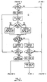
- a flow chart is provided of a controlling computer program that monitors the intensities of the three emission lines and make adjustments in the individual gaseous component flow rates as required to maintain the electron temperature distribution within acceptable limits.
- the process of Figure 7 can best be described as several functional modules.
- a first module 101 requires information of both the desired plasma parameters and those that actually exist. It is preferable to enter a desired average electron temperature T e and then calculate what exists in the plasma, as shown in Figure 7, since this permits the process operator to deal with known quantities. However, since T e is proportional to the ratio of the hydrogen alpha and hydrogen beta emission lines, that ratio itself could more simply be substituted in the flow diagram of Figure 7 where T e appears. It would then be that line intensity ratio to which the process is adjusted.
- a next module 105 of the processing algorithm looks at the intensity ratio between the hydrogen alpha and the helium emission lines.
- a first step 107 compares the actual and desired ratios. If they are within range, then the processing component 105 is omitted completely by jumping to a step 109 in the next module 117. However, if the desired and actual ratios are not equal, a step 111 causes the flow meter 71 to be adjusted to change the flow of silicon source vapour in a direction to move the compared ratios closer together.
- a step 113 of the module 105 checks to make sure that the calculated voltage is within the range of the flow meter 71. If it is, the processing proceeds to a step 109. If not, the process loop of module 105 is performed again. If the second calculation also results in a voltage that is not within the range of the flow meter 71, then the processing is stopped and an error message displayed for the operator, as indicated at 115.
- the next module 117 of the processing adjusts the flow of oxygen to the plasma in response to comparing the desired and actual T e . If those quantities are equal within an acceptable tolerance, then the processing loops back to the beginning module 101 and performs the data acquisition and comparison functions once again, and then steps through the remainder of the program. This constant monitoring of the plasma characteristics allows real time control of the plasma for uniform film results and repeatability of film properties from substrate to substrate.
- the program module 117 operates quite similarly to that of 105. If the newly calculated voltage for the oxygen supply flow meter is not within the range of that flow meter, as determined by the step 119, the calculation is made once more in case some error occurred. If the voltage is not within the range the second time, the processing is stopped and an error message displayed. Assuming, however, that the new oxygen flow meter valve control voltage is within its range, the processing is looped back to the beginning module 101 and repeated until the processing modules 101, 105 and 107 have been performed for a total of four times. After the fourth time, and if the last calculation loop resulted in a further adjustment to the oxygen flow meter, a next module 121 of processing is undertaken. After four times through the silicon source and oxygen flow rate adjustments, it is concluded that some other adjustment must be made. Of course, the precise number of processing cycles that are allowed before going to the next calculation module 121 can vary.
- the module 121 also looks at T e , but in this case adjusts the helium gas flow to the plasma chamber. An increase of the inert gas supply provides more electrons, and a decrease in the gas fewer electrons. The same check on the calculated voltage for the helium flow meter is made in the module 121 as in the modules 105 and 117, in step 123. Once a proper adjustment to the helium flow is made, the processing again loops back to the beginning module 101 to start the cycle over again.
- Plasma input variables of power of the supply 17 and pressure within the chamber 29 are not included in the algorithm of Figure 7 as quantities that are adjusted automatically. It has been found satisfactory to maintain those quantities fixed for at least a large processing batch. This is preferably accomplished by setting the control system 25 to the desired power and pressure.
- the control system 25 is provided with a standard capability of monitoring those quantities and adjusting them, if necessary, to maintain the constant levels that have been set.
- the spectra of the plasma 51 is dependent upon the position within the plasma which is observed. That is, the intensities of the three emission peaks 81, 83 and 85, both absolutely and relatively, are different depending upon where the end of the optical fibre 23 is positioned with respect to the quartz window 24 (Fig. 1) of the reaction chamber 11. So long as this position remains fixed and the intensity distribution across the plasma 51 does not change, the techniques of controlling that process described above optimise it. But if it is desired to use that same process control on a different piece of equipment, for example, it is likely that the plasma will be viewed at a location with a different emission spectrum. Thus, the control system which has been optimised for one plasma emission spectrum may have to be recalibrated to operate with a spectrum having different relative intensities of peaks of interest than in the plasma for which the control system was optimised.
- the spectrum can change across the plasma due to a change in the substrate being coated, primarily in its thickness, any change of gases, gas flow rates, a pumping rate change, some relative change in the electrical power being delivered to the system, and similar matters.
- a technique illustrated with respect to Figs. 8-10 maintains an end of the optical fibre medium 23 to gather light from the same relative position in the plasma, regardless of any such changes.
- the optical fibre 23 is positioned to view the plasma at the location where the ratio of the intensities of emission into relevant narrow band-widths is a maximum. In the example being described, that ratio is preferred to be the intensity of the hydrogen alpha line divided by the intensity of the helium line of emission.
- the optical fibre cable 23 is preferably terminated in a long, small diameter cylindrical tube 301.
- the cable preferably contains dozens of individual optical fibres.
- the purpose of the tube 301 is to limit the natural cone angle of acceptance of light of the optical fibre end so that it accepts substantially collimated light rays emitted from an area of the plasma 51 that is substantially the same size as the size of the opening of the tube 301 at an end adjacent the quartz window 24.
- the inside of the tube 301 is made to be highly reflective.
- the light-guiding tube 301 is attached to a support block 303 that is carried with respect to the reaction chamber 11 in a manner that allows it to be moved in both X and Y directions.
- Appropriate control motors are used to provide such movement.
- An example is the use of separate X and Y direction drive motors 305 and 307, respectively, that drive the support block 303 through respective mechanical connections 309 and 311 to move the block 303 in those two directions.
- the motors 305 and 307 are controlled by position control circuits 313 which are in turn connected to the system computer control 25 (Fig. 1) by an appropriate circuit 315.
- the block 303 can then easily be controlled to move the optical fibre end tube 301 to a position to view the plasma 51 where the ratio of the intensity of the hydrogen alpha line to that of the helium line is a maximum. This adjustment can be made as frequently as each time a substrate is placed into the reaction chamber, or, more practically, on a periodic basis or when the nature of the substrate to be coated significantly changes.
- a number of specific ways of determining the desired location may alternatively be implemented by the mechanism of Figs. 8 and 9.
- One way is to scan the fibre cable tube 301 in some raster pattern across the window 24, while the computer control system 25 calculates a desired ratio from information obtained at several locations of each raster scan line. The location of the block 303 where the ratio is maximised is then determined and the block returned to that position for monitoring the plasma.
- Fig. 10 Another one of many ways of determining the maximum intensity ratio location is illustrated in Fig. 10.
- the tube 301 is located at four spaced apart positions indicated at 317, 319, 321 and 323.
- the ratio of intensities is calculated for each of those locations and the maximum determined. Assuming that maximum in this example was obtained at the location 321, then the tube 301 is positioned at four other locations spaced around the position 321, such as positions 325, 327, 329 and 331.
- the maximum intensity ratio for each of these four locations is noted, and another four locations tested around that location, and so forth.
- the fibre cable tube 301 can be adjusted in some manner by hand, while the operator is observing the desired intensity ratio which is being calculated by the system's computer.
Landscapes
- Chemical & Material Sciences (AREA)
- Engineering & Computer Science (AREA)
- Materials Engineering (AREA)
- Chemical Kinetics & Catalysis (AREA)
- Organic Chemistry (AREA)
- Metallurgy (AREA)
- Mechanical Engineering (AREA)
- General Chemical & Material Sciences (AREA)
- Physics & Mathematics (AREA)
- Fluid Mechanics (AREA)
- Plasma & Fusion (AREA)
- Polymers & Plastics (AREA)
- Medicinal Chemistry (AREA)
- Health & Medical Sciences (AREA)
- Manufacturing & Machinery (AREA)
- Chemical Vapour Deposition (AREA)
- Physical Vapour Deposition (AREA)
- Plasma Technology (AREA)
- Electrodes Of Semiconductors (AREA)
- Light Receiving Elements (AREA)
Claims (16)
- Verfahren zur Steuerung eines Prozesses zum Aufbringen eines dünnen Materialfilms auf ein Substrat in einer Kammer, in der ein Plasma gebildet wird, mit einer Mehrzahl von steuerbaren Prozeßparametern, wobei das Plasma eine Mehrzahl von atomaren und/oder molekularen Spezies mit jeweils einer beobachtbare elektromagnetische Strahlungsemission innerhalb eines sichtbaren oder nahezu sichtbaren Wellenlängenbereichs enthält, deren Art sich bei Veränderung der steuerbaren Prozeßparameter ebenfalls verändert, wobei das Verfahren folgende Schritte aufweist:
Erfassen zweier Charakteristiken der Strahlungsemission einer einzigen Spezies in dem Plasma, wobei diese Charakteristiken sich auf prozeßabhängige Eigenschaften des dünnen Films beziehen,
elektronisches Vergleichen der beiden Charakteristiken, und
Bewirken einer automatischen Veränderung eines oder mehrerer der Prozeßparameter zum Einstellen der beiden erfaßten Strahlungsemissionscharakteristiken der einzelnen Spezies auf einen vorgegebenen gewünschten Zusammenhang. - Verfahren nach Anspruch 1, wobei der Erfassungsschritt das Erfassen der Intensitäten der Emission der einzelnen Spezies in zwei verschiedenen Bandbreitenbereichen als die beiden Charakteristiken umfaßt.
- Verfahren nach Anspruch 1 oder 2, wobei der Vergleichsschritt die elektronische Verhältnisbildung der beiden Intensitäten in den zwei Bandbreitenemissionen umfaßt und wobei der automatische Einstellschritt das Vergleichen dieses Verhältnisses mit einer gewünschten Größe umfaßt.
- Verfahren nach einem der vorhergehenden Ansprüche, das einen zusätzlichen Schritt des Erfassens einer Intensität einer definierten Emissionsbandbreite einer anderen Spezies in dem Plasma aufweist.
- Verfahren zur Steuerung eines Prozesses zum Aufbringen eines dünnen Materialfilms auf ein Substrat in einer Kammer, in welcher ein Plasma gebildet wird, mit einer Mehrzahl von steuerbaren Prozeßparametern, die Druck und individuelle Strömungsdurchsätze von zwei oder mehr Gasen in die Kammer und ein elektrisches Feld umfassen, wobei das Verfahren die folgenden Schritte aufweist:
Erfassen der Intensität von jeweils zwei schmalbandigen Linien der sichtbaren oder nahezu sichtbaren elektromagnetischen Strahlungsemission von einer einzigen Spezies in dem Plasma,
elektronisches Berechnen des Verhältnisses der Wellenlängenbandintensitäten,
elektronisches Vergleichen des Verhältnisses mit einem gewünschten Verhältnis, das während des Aufbringprozesses aufrechtzuerhalten ist, und
Bewirken der automatischen Veränderung eines oder mehrerer der Prozeßparameter zum Einstellen des berechneten Verhältnisses zur Verringerung einer etwaigen Differenz zwischen den berechneten und dem gewünschtem Verhältnis. - Verfahren nach Anspruch 5, das zusätzlich folgende Schritte aufweist:
Erfassen der Intensität einer schmalbandigen Linie der sichtbaren oder nahezu sichtbaren elektromagnetischen Strahlungsemission von einer weiteren Spezies, die sich von einem Energiepegel ergibt, der höher als derjenige der erfaßten Linien der genannten einzelnen Spezies ist,
elektronisches Berechnen eines zweiten Verhältnisses von Emissionslinienintensitäten, wobei das zweite Verhältnis zwischen der Intensität einer der beiden Emissionslinien der einzelnen Spezies und der Intensität der Emissionslinie der anderen Spezies liegt,
elektronisches Vergleichen des zweiten berechneten Verhältnisses und eines zweiten gewünschten Verhältnisses, das während des Aufbringprozesses aufrechterhalten werden soll, und
Bewirken der automatischen Veränderung eines oder mehrerer der Prozeßparameter zum Einstellen des zweiten berechneten Verhältnisses zur Verringerung einer etwaigen Differenz zwischen den berechneten und dem gewünschten zweiten Verhältnis. - Verfahren nach Anspruch 6, bei welchem die weitere Spezies aus einem Inertgas besteht.
- Verfahren nach einem der Ansprüche 5 bis 7, bei welchem der Einstellschritt den Schritt der automatischen Veränderung des Strömungsdurchsatzes mindestens eines der Gase in die Kammer umfaßt.
- Verfahren nach einem der Ansprüche 6 bis 8, bei welchem der Einstellschritt für das zweite Verhältnis den Schritt der automatischen Veränderung des Strömungsdurchsatzes mindestens eines der Gase in die Kammer umfaßt.
- Verfahren nach einem der Ansprüche 6 bis 9, bei welchem der Vergleichsschritt den Schritt der Berechnung der mittleren Elektronentemperatur des Plasmas aus dem Intensitätsverhältnis umfaßt.
- Prozeß zum Aufbringen eines dünnen Materialfilms auf ein Substrat in einer Kammer, in welcher ein Plasma in einem Bereich magnetischer und elektrischer Felder als Ergebnis des Zuströmens mindestens eines ersten und eines zweiten Gases in die Kammer gebildet wird, mit folgenden Schritten:
Erfassen eines ersten und eines zweiten Intensitätspegels von jeweils zwei schmalbandigen Linien sichtbarer oder nahezu sichtbarer elektromagnetischer Strahlungsemission aus einer einzigen Spezies des Plasmas,
Erfassen eines dritten Intensitätspegels einer schmalbandigen Linie sichtbarer oder nahezu sichtbarer elektromagnetischer Strahlungsemission von einer weiteren Spezies, die sich aus einem Energiepegel ergibt, der höher als derjenige der erfaßten Linien der einzelnen Spezies ist,
elektronisches Gewinnen eines ersten Verhältnisses des ersten und des zweiten Intensitätspegels,
elektronisches Gewinnen eines zweiten Verhältnisses des ersten und des dritten Intensitätspegels,
Einstellen des Strömungsdurchsatzes des ersten Gases in die Kammer in solcher Weise, daß das erste Verhältnis auf einem ersten vorgegebenen Wert gehalten wird, und
Einstellen des Strömungsdurchsatzes des zweiten Gases in die Kammer in solcher Weise, daß das zweite Verhältnis auf einem zweiten vorgegebenen Wert gehalten wird. - Verfahren nach Anspruch 11, bei welchem das erste Gas durch Moleküle gekennzeichnet ist, in welchem die einzelne Spezies in solcher Weise enthalten ist, daß sie sich in dem Plasma von den Molekülen abspaltet, die weitere Spezies durch Inertheit gekennzeichnet ist, und das zweite Gas durch eine Veränderung der mittleren Elektronenenergie im Plasma gekennzeichnet ist.
- Prozeß nach Anspruch 11 oder 12, bei welchem das erste Gas einen Organosilikondampf und das zweite Gas Sauerstoff enthält.
- Verfahren nach einem der Ansprüche 11 bis 13, bei welchem die Intensitätspegelerfassungsschritte die Erfassung der Plasmaemissionsintensität aus einem Plasmabereich umfassen, bei welchem das zweite Intensitätsverhältnis im wesentlichen ein Maximum erreicht.
- Verfahren zur Bestimmung des Elektronentemperaturpegels in einem Plasma, mit folgenden Schritten:
Erfassen der Intensität jeweils zweier schmalbandiger Linien sichtbarer oder nahezu sichtbarer elektromagnetischer Strahlungsemission von einer einzigen Spezies in dem Plasma,
elektronisches Berechnen des Verhältnisses der Wellenlängenbandintensitäten, und
elektronisches Berechnen eines Schätzwerts der mittleren Elektronentemperatur des Plasmas aus dem Verhältnis. - Verfahren nach einem der vorhergehenden Ansprüche, wobei die Strahlungsemission im ultravioletten Bereich liegt.
Applications Claiming Priority (4)
| Application Number | Priority Date | Filing Date | Title |
|---|---|---|---|
| US7392887A | 1987-07-15 | 1987-07-15 | |
| US73928 | 1987-07-15 | ||
| US07/191,448 US4888199A (en) | 1987-07-15 | 1988-05-09 | Plasma thin film deposition process |
| US191448 | 2002-07-10 |
Publications (3)
| Publication Number | Publication Date |
|---|---|
| EP0299752A2 EP0299752A2 (de) | 1989-01-18 |
| EP0299752A3 EP0299752A3 (en) | 1990-04-11 |
| EP0299752B1 true EP0299752B1 (de) | 1994-08-31 |
Family
ID=26755049
Family Applications (1)
| Application Number | Title | Priority Date | Filing Date |
|---|---|---|---|
| EP88306431A Expired - Lifetime EP0299752B1 (de) | 1987-07-15 | 1988-07-13 | Kontrolle eines Verfahrens zur Abscheidung eines dünnen Filmes mittels Plasma |
Country Status (13)
| Country | Link |
|---|---|
| US (1) | US4888199A (de) |
| EP (1) | EP0299752B1 (de) |
| JP (1) | JP2539000B2 (de) |
| KR (1) | KR910009981B1 (de) |
| CN (1) | CN1024814C (de) |
| AT (1) | ATE110794T1 (de) |
| AU (1) | AU616894B2 (de) |
| CA (1) | CA1329166C (de) |
| DE (1) | DE3851281T2 (de) |
| ES (1) | ES2059523T3 (de) |
| MX (1) | MX171506B (de) |
| RU (1) | RU1797628C (de) |
| UA (1) | UA18259A (de) |
Families Citing this family (59)
| Publication number | Priority date | Publication date | Assignee | Title |
|---|---|---|---|---|
| US5348736A (en) | 1989-06-21 | 1994-09-20 | Colgate-Palmolive Company | Stabilized hair-treating compositions |
| LU87880A1 (fr) * | 1991-01-24 | 1992-10-15 | Europ Communities | Methode permettant de deposer une couche mince par photo-ablation |
| MX9303141A (es) * | 1992-05-28 | 1994-04-29 | Polar Materials Inc | Metodos y aparatos para depositar recubrimientos de barrera. |
| DE4320931A1 (de) * | 1992-10-21 | 1994-04-28 | Solvay Deutschland | Abscheidung von Schichten mit hoher spezifischer elektrischer Leitfähigkeit |
| US5395642A (en) * | 1992-10-21 | 1995-03-07 | Solvay Deutschland Gmbh | Process for depositing layers having high specific electrical conductivity |
| US5240736A (en) * | 1992-10-26 | 1993-08-31 | Ford Motor Company | Method and apparatus for in-situ measuring filament temperature and the thickness of a diamond film |
| US5429730A (en) * | 1992-11-02 | 1995-07-04 | Kabushiki Kaisha Toshiba | Method of repairing defect of structure |
| CH685755A5 (de) * | 1993-06-03 | 1995-09-29 | Tetra Pak Suisse Sa | Verfahren zur Herstellung eines Schichtstoffes. |
| CA2123479C (en) * | 1993-07-01 | 1999-07-06 | Peter A. Sieck | Anode structure for magnetron sputtering systems |
| US5534066A (en) * | 1993-10-29 | 1996-07-09 | International Business Machines Corporation | Fluid delivery apparatus having an infrared feedline sensor |
| CN1152979C (zh) * | 1993-10-29 | 2004-06-09 | 巴尔策斯有限公司 | 镀膜物体、其制备方法和用途 |
| CH687601A5 (de) * | 1994-02-04 | 1997-01-15 | Tetra Pak Suisse Sa | Verfahren zur Herstellung von im Innern sterilen Verpackungen mit hervorragenden Sperreigenschaften. |
| CH687614A5 (de) * | 1994-02-04 | 1997-01-15 | Tetra Pak Suisse Sa | Verfahren zum Versehen einer Verpackung mit hervorragenden Sperreigenschaften in bezug auf Gase. |
| US6149982A (en) * | 1994-02-16 | 2000-11-21 | The Coca-Cola Company | Method of forming a coating on an inner surface |
| WO1995022413A1 (en) | 1994-02-16 | 1995-08-24 | The Coca-Cola Company | Hollow containers with inert or impermeable inner surface through plasma-assisted surface reaction or on-surface polymerization |
| US5571470A (en) * | 1994-02-18 | 1996-11-05 | The Coca-Cola Company | Method for fabricating a thin inner barrier layer within a preform |
| US5741505A (en) * | 1995-01-20 | 1998-04-21 | Mars, Incorporated | Edible products having inorganic coatings |
| US5685797A (en) * | 1995-05-17 | 1997-11-11 | United Technologies Corporation | Coated planet gear journal bearing and process of making same |
| US5788869A (en) * | 1995-11-02 | 1998-08-04 | Digital Equipment Corporation | Methodology for in situ etch stop detection and control of plasma etching process and device design to minimize process chamber contamination |
| US5658423A (en) * | 1995-11-27 | 1997-08-19 | International Business Machines Corporation | Monitoring and controlling plasma processes via optical emission using principal component analysis |
| US5968324A (en) * | 1995-12-05 | 1999-10-19 | Applied Materials, Inc. | Method and apparatus for depositing antireflective coating |
| US6127262A (en) | 1996-06-28 | 2000-10-03 | Applied Materials, Inc. | Method and apparatus for depositing an etch stop layer |
| DE19629877C1 (de) * | 1996-07-24 | 1997-03-27 | Schott Glaswerke | CVD-Verfahren und Vorrichtung zur Innenbeschichtung von Hohlkörpern |
| US6223683B1 (en) * | 1997-03-14 | 2001-05-01 | The Coca-Cola Company | Hollow plastic containers with an external very thin coating of low permeability to gases and vapors through plasma-assisted deposition of inorganic substances and method and system for making the coating |
| US5778681A (en) * | 1997-04-15 | 1998-07-14 | Varian Associates, Inc. | Cooling device for cooling heatable gas chromatography analyte sample injector |
| JPH1129863A (ja) * | 1997-07-10 | 1999-02-02 | Canon Inc | 堆積膜製造方法 |
| US8075789B1 (en) * | 1997-07-11 | 2011-12-13 | Applied Materials, Inc. | Remote plasma cleaning source having reduced reactivity with a substrate processing chamber |
| AU8762398A (en) * | 1997-08-08 | 1999-03-01 | Lockheed Martin Corporation | Multi-spectroscopic emission line control for thin film sputtering process |
| US6024831A (en) * | 1997-08-20 | 2000-02-15 | Vanguard International Semiconductor Corporation | Method and apparatus for monitoring plasma chamber condition by observing plasma stability |
| US6203898B1 (en) * | 1997-08-29 | 2001-03-20 | 3M Innovatave Properties Company | Article comprising a substrate having a silicone coating |
| US6106676A (en) * | 1998-04-16 | 2000-08-22 | The Boc Group, Inc. | Method and apparatus for reactive sputtering employing two control loops |
| US6251233B1 (en) | 1998-08-03 | 2001-06-26 | The Coca-Cola Company | Plasma-enhanced vacuum vapor deposition system including systems for evaporation of a solid, producing an electric arc discharge and measuring ionization and evaporation |
| TW409383B (en) * | 1998-12-31 | 2000-10-21 | World Wiser Electronics Inc | Apparatus of plug hole process and the method thereof |
| US6366353B1 (en) * | 1999-11-05 | 2002-04-02 | Corning Incorporated | Method to determine the identity of a material in an object |
| TW413726B (en) * | 1999-11-20 | 2000-12-01 | Prec Instr Dev Ct | Method for monitoring thickness uniformity of films based on spectroscopic measurement |
| US6455098B2 (en) * | 2000-03-09 | 2002-09-24 | Semix Incorporated | Wafer processing apparatus and method |
| US6720052B1 (en) * | 2000-08-24 | 2004-04-13 | The Coca-Cola Company | Multilayer polymeric/inorganic oxide structure with top coat for enhanced gas or vapor barrier and method for making same |
| US6740378B1 (en) | 2000-08-24 | 2004-05-25 | The Coca-Cola Company | Multilayer polymeric/zero valent material structure for enhanced gas or vapor barrier and uv barrier and method for making same |
| US6613656B2 (en) * | 2001-02-13 | 2003-09-02 | Micron Technology, Inc. | Sequential pulse deposition |
| US6599584B2 (en) * | 2001-04-27 | 2003-07-29 | The Coca-Cola Company | Barrier coated plastic containers and coating methods therefor |
| ATE309291T1 (de) * | 2002-04-15 | 2005-11-15 | Coca Cola Co | Beschichtungszusammensetzung enthaltend einen epoxyzusatz und damit beschichtete strukturen |
| GB0222331D0 (en) * | 2002-09-26 | 2002-10-30 | Teer Coatings Ltd | A method for depositing multilayer coatings with controlled thickness |
| US8062716B2 (en) * | 2002-09-30 | 2011-11-22 | Toppan Printing Co., Ltd. | Method for forming thin film, apparatus for forming thin film, and method for monitoring thin film forming process |
| US6879744B2 (en) * | 2003-01-07 | 2005-04-12 | Georgi A. Atanasov | Optical monitoring of thin film deposition |
| US20050266173A1 (en) * | 2004-05-26 | 2005-12-01 | Tokyo Electron Limited | Method and apparatus of distributed plasma processing system for conformal ion stimulated nanoscale deposition process |
| FR2892854A1 (fr) * | 2005-10-27 | 2007-05-04 | Sidel Sas | Methode de surveillance d'un plasma, dispositif pour la mise en oeuvre de cette methode, application de cette methode au depot d'un film sur corps creux en pet |
| CN1851420B (zh) * | 2005-12-08 | 2010-12-08 | 北京北方微电子基地设备工艺研究中心有限责任公司 | 一种等离子体内电子温度测量装置 |
| US20090130362A1 (en) * | 2007-11-21 | 2009-05-21 | Egan Visual Inc. | Multiuse dry erase writing and projection surface |
| US9997325B2 (en) * | 2008-07-17 | 2018-06-12 | Verity Instruments, Inc. | Electron beam exciter for use in chemical analysis in processing systems |
| RU2413330C1 (ru) * | 2009-11-23 | 2011-02-27 | Закрытое акционерное общество "Нанотех-Актив" | Способ получения атомно-тонких монокристаллических пленок |
| US8304262B2 (en) * | 2011-02-17 | 2012-11-06 | Lam Research Corporation | Wiggling control for pseudo-hardmask |
| DE102011051226A1 (de) * | 2011-06-21 | 2012-12-27 | Q-Cells Se | Plasma-unterstütztes Abscheideverfahren und Vorrichtung zu dessen Durchführung |
| TWI495746B (zh) * | 2013-11-13 | 2015-08-11 | Mingdao University | 沉積系統 |
| JP6158111B2 (ja) * | 2014-02-12 | 2017-07-05 | 東京エレクトロン株式会社 | ガス供給方法及び半導体製造装置 |
| CN111133609B (zh) * | 2017-09-20 | 2022-11-25 | 应用材料公司 | 处理腔室以及用于形成电化学能储存装置的元件的陶瓷层的方法、蒸发源 |
| CN110632973B (zh) * | 2019-09-24 | 2021-07-09 | 中国航空工业集团公司沈阳飞机设计研究所 | 一种电磁辐射控制方法及其装置 |
| CN114622183A (zh) * | 2020-12-11 | 2022-06-14 | 湖南红太阳光电科技有限公司 | 一种制备氧化硅薄膜的方法 |
| RU2765222C1 (ru) * | 2020-12-30 | 2022-01-26 | Тхе Баттериес Сп. з о.о. | Способ формирования пленки LiCoO2 и устройство для его реализации |
| CN114615786B (zh) * | 2022-01-28 | 2024-07-23 | 北京控制工程研究所 | 一种磁响应磁等离子体动力推力器阴极及其制备方法 |
Family Cites Families (6)
| Publication number | Priority date | Publication date | Assignee | Title |
|---|---|---|---|---|
| US4006404A (en) * | 1976-01-30 | 1977-02-01 | The United States Of America As Represented By The Secretary Of The Navy | Pulsed plasma probe |
| DE2947542A1 (de) * | 1979-11-26 | 1981-06-04 | Leybold-Heraeus GmbH, 5000 Köln | Einrichtung zur ueberwachung und/oder steuerung von plasmaprozessen |
| FR2586156A1 (fr) * | 1985-08-07 | 1987-02-13 | Hochvakuum Dresden Veb | Procede pour regler la densite de vapeur dans des processus de revetement utilisant un plasma avec des evaporateurs a decharge d'arc, et dispositif correspondant pour revetir des substrats a l'aide de plasma |
| GB2181461B (en) * | 1985-10-10 | 1989-09-27 | Canadian Patents Dev | Doping semiconductor compounds by reactive sputtering |
| JPS6289869A (ja) * | 1985-10-15 | 1987-04-24 | Sumitomo Electric Ind Ltd | 硬質炭素膜の気相合成法 |
| JPS6293382A (ja) * | 1985-10-21 | 1987-04-28 | Mitsubishi Electric Corp | 薄膜形成装置 |
-
1988
- 1988-05-09 US US07/191,448 patent/US4888199A/en not_active Expired - Fee Related
- 1988-07-11 MX MX1222388A patent/MX171506B/es unknown
- 1988-07-13 AU AU19012/88A patent/AU616894B2/en not_active Ceased
- 1988-07-13 EP EP88306431A patent/EP0299752B1/de not_active Expired - Lifetime
- 1988-07-13 AT AT88306431T patent/ATE110794T1/de not_active IP Right Cessation
- 1988-07-13 ES ES88306431T patent/ES2059523T3/es not_active Expired - Lifetime
- 1988-07-13 DE DE3851281T patent/DE3851281T2/de not_active Expired - Fee Related
- 1988-07-14 UA UA4356339A patent/UA18259A/uk unknown
- 1988-07-14 CA CA000571973A patent/CA1329166C/en not_active Expired - Fee Related
- 1988-07-14 RU SU884356339A patent/RU1797628C/ru active
- 1988-07-14 KR KR1019880008852A patent/KR910009981B1/ko not_active Expired
- 1988-07-15 CN CN88104424A patent/CN1024814C/zh not_active Expired - Fee Related
- 1988-07-15 JP JP63176851A patent/JP2539000B2/ja not_active Expired - Lifetime
Also Published As
| Publication number | Publication date |
|---|---|
| KR910009981B1 (ko) | 1991-12-09 |
| CN1024814C (zh) | 1994-06-01 |
| CN1030615A (zh) | 1989-01-25 |
| UA18259A (uk) | 1997-12-25 |
| AU616894B2 (en) | 1991-11-14 |
| EP0299752A2 (de) | 1989-01-18 |
| ATE110794T1 (de) | 1994-09-15 |
| ES2059523T3 (es) | 1994-11-16 |
| EP0299752A3 (en) | 1990-04-11 |
| US4888199A (en) | 1989-12-19 |
| KR890002287A (ko) | 1989-04-10 |
| RU1797628C (ru) | 1993-02-23 |
| AU1901288A (en) | 1989-01-19 |
| DE3851281D1 (de) | 1994-10-06 |
| JP2539000B2 (ja) | 1996-10-02 |
| MX171506B (es) | 1993-11-03 |
| DE3851281T2 (de) | 1995-04-13 |
| CA1329166C (en) | 1994-05-03 |
| JPS6487777A (en) | 1989-03-31 |
Similar Documents
| Publication | Publication Date | Title |
|---|---|---|
| AU616894B2 (en) | Plasma thin film deposition process control | |
| EP0469926A1 (de) | Dünnschicht-Dampfsperren auf Siliziumoxidbasis | |
| US5904952A (en) | Method of plasma enhanced silicon oxide deposition | |
| Ryan et al. | Plasma polymerization of sputtered poly (tetrafluoroethylene) | |
| US5614248A (en) | Method for plasma-assisted reactive electron beam vaporization | |
| JPH0216733A (ja) | 半導体プロセッシングにおけるプラズマ特性の測定方法 | |
| US20190360923A1 (en) | System and method for monitoring atomic absorption during a surface modification process | |
| US20090120581A1 (en) | Systems and methods for plasma processing of microfeature workpieces | |
| DE19824364A1 (de) | Verfahren zum Aufbringen eines Verschleißschutz-Schichtsystems mit optischen Eigenschaften auf Oberflächen | |
| Cruden et al. | Time resolved ultraviolet absorption spectroscopy of pulsed fluorocarbon plasmas | |
| Clark et al. | Plasma polymerization. IV. A systematic investigation of the inductively coupled RF plasma polymerization of pentafluorobenzene. | |
| JP3511089B2 (ja) | 低温プラズマによる固体表面処理制御方法 | |
| US6903800B2 (en) | Film-processing method and film-processing apparatus | |
| US6493070B1 (en) | Method for in-situ monitoring layer uniformity of sputter coating based on intensity distribution of plasma spectrum | |
| Baravian et al. | Optical emission spectroscopy of active species in a TiCN PVD arc discharge | |
| Galyautdinov et al. | Technology of sputtering high-reflection coatings on ABS-plastic articles | |
| Zak et al. | Vinyl-based interlayers synthesized by variable pulsed plasma for polymer composites | |
| Meichsner | In situ characterisation of polymer surfaces and thin organic films in plasma processing | |
| Clark et al. | An investigation of the vacuum UV spectra of inductivity coupled RF plasmas excited in inert gases as a function of some of the operating parameters | |
| JPH059728A (ja) | 薄膜形成方法 | |
| Lee et al. | In situ monitoring of the relative distribution of radicals by a two probe system | |
| Stalder et al. | Mass spectroscopic investigations of a hydrocarbon arcjet plasma operating under diamond deposition conditions | |
| Stojcevski et al. | Broadband optical monitoring for a 2-meter optics magnetron sputtering deposition machine | |
| Koch et al. | In situ plasma and surface diagnostics of C: H deposition from ECR plasmas | |
| Ibrahim et al. | Optical thin films deposition by MDECR-PECVD |
Legal Events
| Date | Code | Title | Description |
|---|---|---|---|
| PUAI | Public reference made under article 153(3) epc to a published international application that has entered the european phase |
Free format text: ORIGINAL CODE: 0009012 |
|
| AK | Designated contracting states |
Kind code of ref document: A2 Designated state(s): AT BE CH DE ES FR GB IT LI LU NL SE |
|
| PUAL | Search report despatched |
Free format text: ORIGINAL CODE: 0009013 |
|
| AK | Designated contracting states |
Kind code of ref document: A3 Designated state(s): AT BE CH DE ES FR GB IT LI LU NL SE |
|
| 17P | Request for examination filed |
Effective date: 19900529 |
|
| 17Q | First examination report despatched |
Effective date: 19910725 |
|
| GRAA | (expected) grant |
Free format text: ORIGINAL CODE: 0009210 |
|
| ITF | It: translation for a ep patent filed | ||
| AK | Designated contracting states |
Kind code of ref document: B1 Designated state(s): AT BE CH DE ES FR GB IT LI LU NL SE |
|
| REF | Corresponds to: |
Ref document number: 110794 Country of ref document: AT Date of ref document: 19940915 Kind code of ref document: T |
|
| ET | Fr: translation filed | ||
| REF | Corresponds to: |
Ref document number: 3851281 Country of ref document: DE Date of ref document: 19941006 |
|
| REG | Reference to a national code |
Ref country code: ES Ref legal event code: FG2A Ref document number: 2059523 Country of ref document: ES Kind code of ref document: T3 |
|
| EAL | Se: european patent in force in sweden |
Ref document number: 88306431.3 |
|
| PGFP | Annual fee paid to national office [announced via postgrant information from national office to epo] |
Ref country code: AT Payment date: 19950619 Year of fee payment: 8 |
|
| PLBE | No opposition filed within time limit |
Free format text: ORIGINAL CODE: 0009261 |
|
| STAA | Information on the status of an ep patent application or granted ep patent |
Free format text: STATUS: NO OPPOSITION FILED WITHIN TIME LIMIT |
|
| 26N | No opposition filed | ||
| PG25 | Lapsed in a contracting state [announced via postgrant information from national office to epo] |
Ref country code: AT Effective date: 19960713 |
|
| PGFP | Annual fee paid to national office [announced via postgrant information from national office to epo] |
Ref country code: SE Payment date: 19970619 Year of fee payment: 10 |
|
| PGFP | Annual fee paid to national office [announced via postgrant information from national office to epo] |
Ref country code: FR Payment date: 19970620 Year of fee payment: 10 |
|
| PGFP | Annual fee paid to national office [announced via postgrant information from national office to epo] |
Ref country code: DE Payment date: 19970624 Year of fee payment: 10 Ref country code: CH Payment date: 19970624 Year of fee payment: 10 |
|
| PGFP | Annual fee paid to national office [announced via postgrant information from national office to epo] |
Ref country code: NL Payment date: 19970625 Year of fee payment: 10 |
|
| PGFP | Annual fee paid to national office [announced via postgrant information from national office to epo] |
Ref country code: GB Payment date: 19970626 Year of fee payment: 10 Ref country code: BE Payment date: 19970626 Year of fee payment: 10 |
|
| PGFP | Annual fee paid to national office [announced via postgrant information from national office to epo] |
Ref country code: ES Payment date: 19970717 Year of fee payment: 10 |
|
| PGFP | Annual fee paid to national office [announced via postgrant information from national office to epo] |
Ref country code: LU Payment date: 19971007 Year of fee payment: 10 |
|
| PG25 | Lapsed in a contracting state [announced via postgrant information from national office to epo] |
Ref country code: LU Free format text: LAPSE BECAUSE OF NON-PAYMENT OF DUE FEES Effective date: 19980713 Ref country code: GB Free format text: LAPSE BECAUSE OF NON-PAYMENT OF DUE FEES Effective date: 19980713 |
|
| PG25 | Lapsed in a contracting state [announced via postgrant information from national office to epo] |
Ref country code: SE Free format text: LAPSE BECAUSE OF NON-PAYMENT OF DUE FEES Effective date: 19980714 Ref country code: ES Free format text: LAPSE BECAUSE OF THE APPLICANT RENOUNCES Effective date: 19980714 |
|
| PG25 | Lapsed in a contracting state [announced via postgrant information from national office to epo] |
Ref country code: LI Free format text: LAPSE BECAUSE OF NON-PAYMENT OF DUE FEES Effective date: 19980731 Ref country code: CH Free format text: LAPSE BECAUSE OF NON-PAYMENT OF DUE FEES Effective date: 19980731 Ref country code: BE Free format text: LAPSE BECAUSE OF NON-PAYMENT OF DUE FEES Effective date: 19980731 |
|
| BERE | Be: lapsed |
Owner name: THE BOC GROUP INC. Effective date: 19980731 |
|
| PG25 | Lapsed in a contracting state [announced via postgrant information from national office to epo] |
Ref country code: NL Free format text: LAPSE BECAUSE OF NON-PAYMENT OF DUE FEES Effective date: 19990201 |
|
| GBPC | Gb: european patent ceased through non-payment of renewal fee |
Effective date: 19980713 |
|
| REG | Reference to a national code |
Ref country code: CH Ref legal event code: PL |
|
| EUG | Se: european patent has lapsed |
Ref document number: 88306431.3 |
|
| PG25 | Lapsed in a contracting state [announced via postgrant information from national office to epo] |
Ref country code: FR Free format text: LAPSE BECAUSE OF NON-PAYMENT OF DUE FEES Effective date: 19990331 |
|
| NLV4 | Nl: lapsed or anulled due to non-payment of the annual fee |
Effective date: 19990201 |
|
| PG25 | Lapsed in a contracting state [announced via postgrant information from national office to epo] |
Ref country code: DE Free format text: LAPSE BECAUSE OF NON-PAYMENT OF DUE FEES Effective date: 19990501 |
|
| REG | Reference to a national code |
Ref country code: FR Ref legal event code: ST |
|
| REG | Reference to a national code |
Ref country code: ES Ref legal event code: FD2A Effective date: 20001009 |
|
| PG25 | Lapsed in a contracting state [announced via postgrant information from national office to epo] |
Ref country code: IT Free format text: LAPSE BECAUSE OF NON-PAYMENT OF DUE FEES;WARNING: LAPSES OF ITALIAN PATENTS WITH EFFECTIVE DATE BEFORE 2007 MAY HAVE OCCURRED AT ANY TIME BEFORE 2007. THE CORRECT EFFECTIVE DATE MAY BE DIFFERENT FROM THE ONE RECORDED. Effective date: 20050713 |