EP0295802B1 - Flüssigkristall-Anzeige - Google Patents
Flüssigkristall-Anzeige Download PDFInfo
- Publication number
- EP0295802B1 EP0295802B1 EP88304847A EP88304847A EP0295802B1 EP 0295802 B1 EP0295802 B1 EP 0295802B1 EP 88304847 A EP88304847 A EP 88304847A EP 88304847 A EP88304847 A EP 88304847A EP 0295802 B1 EP0295802 B1 EP 0295802B1
- Authority
- EP
- European Patent Office
- Prior art keywords
- liquid crystal
- crystal display
- frames
- polarity
- display device
- Prior art date
- Legal status (The legal status is an assumption and is not a legal conclusion. Google has not performed a legal analysis and makes no representation as to the accuracy of the status listed.)
- Expired
Links
- 239000004973 liquid crystal related substance Substances 0.000 title claims description 46
- 239000011159 matrix material Substances 0.000 claims description 9
- 230000000694 effects Effects 0.000 claims description 2
- 238000000034 method Methods 0.000 description 28
- 239000000758 substrate Substances 0.000 description 7
- 239000013256 coordination polymer Substances 0.000 description 3
- 238000010586 diagram Methods 0.000 description 2
- 239000007788 liquid Substances 0.000 description 2
- 238000012986 modification Methods 0.000 description 2
- 230000004048 modification Effects 0.000 description 2
- 230000000717 retained effect Effects 0.000 description 2
- 238000010276 construction Methods 0.000 description 1
- 210000002858 crystal cell Anatomy 0.000 description 1
- 230000001788 irregular Effects 0.000 description 1
Images


Classifications
-
- G—PHYSICS
- G09—EDUCATION; CRYPTOGRAPHY; DISPLAY; ADVERTISING; SEALS
- G09G—ARRANGEMENTS OR CIRCUITS FOR CONTROL OF INDICATING DEVICES USING STATIC MEANS TO PRESENT VARIABLE INFORMATION
- G09G3/00—Control arrangements or circuits, of interest only in connection with visual indicators other than cathode-ray tubes
- G09G3/20—Control arrangements or circuits, of interest only in connection with visual indicators other than cathode-ray tubes for presentation of an assembly of a number of characters, e.g. a page, by composing the assembly by combination of individual elements arranged in a matrix no fixed position being assigned to or needed to be assigned to the individual characters or partial characters
- G09G3/34—Control arrangements or circuits, of interest only in connection with visual indicators other than cathode-ray tubes for presentation of an assembly of a number of characters, e.g. a page, by composing the assembly by combination of individual elements arranged in a matrix no fixed position being assigned to or needed to be assigned to the individual characters or partial characters by control of light from an independent source
- G09G3/36—Control arrangements or circuits, of interest only in connection with visual indicators other than cathode-ray tubes for presentation of an assembly of a number of characters, e.g. a page, by composing the assembly by combination of individual elements arranged in a matrix no fixed position being assigned to or needed to be assigned to the individual characters or partial characters by control of light from an independent source using liquid crystals
- G09G3/3611—Control of matrices with row and column drivers
- G09G3/3614—Control of polarity reversal in general
Definitions
- the present invention relates to a liquid crystal display device containing an X-Y matrix type liquid crystal display panel.
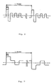
- an X-Y matrix type liquid crystal display panel is driven in either of the following two well-known methods: so-called A method (e.g. EP-A-0 216 168) in which the polarity of applied voltage is reversed in one horizontal scanning period as shown in Fig. 6, and so-called B method in which the polarity of applied voltage is reversed for each frame as shown in Fig. 7.
- a method e.g. EP-A-0 216 168
- B method in which the polarity of applied voltage is reversed for each frame as shown in Fig. 7.
- the waveforms shown in Figs. 6 and 7 include waveform distortion caused by the electrostatic capacity of the liquid crystal panel and by the resistance of the transparent electrodes.
- the A method provides a smaller ratio of waveform frequency variation by display pattern than the B method does (the frequency change ratio is 2 in the A method whereas it is N in the B method when the duty ratio is N), but provides higher frequency in general, resulting in larger power consumption.
- the A method is influenced significantly by waveform distortion so that the effective applied voltage drops. Because of this reason, the A method is hardly used for large liquid crystal display panels.
- an X-Y matrix type liquid crystal display panel is driven mostly by the B method.
- the B method tends to cause irregular picture and crosstalk which deteriorates the picture quality seriously.
- Fig. 8 shows a typical crosstalk phenomenon. It is shown that a pattern where black portions 2 should be normally displayed against the white background 1 suffers crosstalk so that portion 3 which should be white become gray.
- the driving waveforms for the portions 1 and 3 are shown in Figs. 9(1) and 9(2), respectively.
- the driving frequency component by the display pattern is mainly low frequency
- the driving frequency component by the display pattern is mainly high frequency.
- the difference in the frequency component of the driving waveforms results in a conspicuous crosstalk phenomenon.
- crosstalk can be caused by the diversified frequency characteristic of the threshold voltage of the liquid crystal display panel or by the variation of effective voltage caused by distorted driving waveform.
- the former cause occurs when the threshold voltage of the liquid crystal display panel changes in a driving frequency band although the effective voltage is constant.
- the driving frequency band varies depending upon the driving method.
- the frequency variation ratios of the conventional A and B methods are 2 and N (N is a duty ratio), respectively.
- N is a duty ratio
- a driving method from which the above problems are eliminated has been proposed.
- the proposed method is to reverse the polarity of driving voltage applied to the liquid crystal display panel at intervals of specified horizontal scanning periods. According to this method, the advantage of the B method can be made use of, while power consumption is minimized.
- the driving waveforms in which the polarity of the waveforms of Figs. 9(1) and 9(2) is reversed every four horizontal scanning periods (4H) are shown in Figs. 10(1) and 10(2), respectively.
- the frequency of polarity reversing signal is the major component of the driving frequency, so that the influence by the frequency by display pattern is reduced.
- the driving frequency having a low frequency component near the frame frequency is shifted to the higher frequency side so as to contract and equalize the driving frequency component for each picture element.
- the waveform distortion is also equalized as shown in Fig. 10, and the effective voltage value is levelled to some extent in this method.
- the above proposed method has an effect of reducing crosstalk phenomenon. But it has another problem that linear display irregularity is generated along the scanning lines when polarity is reversed. This display irregularity is caused by the following reason.
- Figs. 11(1) through 11(5) show examples of driving waveforms in the liquid crystal display device.
- waveform distortion caused by the electrostatic capacity of the liquid crystal panel and by the resistance of the transparent electrodes is also taken into account.
- Figs. 11(1) and 11(2) show the waveform of driving voltage applied to the scanning electrodes.
- the waveform of Fig. 11(1) is for the case where a selection pulse is generated immediately after the reversal of polarity
- the waveform of Fig. 11(2) is for another case.
- Fig. 11(3) shows the waveform of driving voltage applied to the signal electrodes. This waveform is for the case where all picture elements are turned off.
- Fig. 11(4) shows the potential difference between the waveform of Fig. 11(1) and that of Fig. 11(3)
- Fig. 11(5) shows the potential difference between the waveform of Fig. 11(2) and that of Fig. 11(3). Both are the waveforms of voltage applied to the picture elements. As shown, waveform distortion is different between Fig.
- crosstalk occurs in the conventional liquid crystal display device, and if measure is taken to eliminate the crosstalk, linear display irregularity or meandering phenomenon is observed on the screen.
- an object of the present invention is to provide a liquid crystal display device capable of producing a uniform and high quality display.
- Another object of the present invention is to provide a liquid crystal display device driving method which realizes a uniform and high quality display free from crosstalk, display irregularity and meandering phenomenon.
- a liquid crystal display device comprises an X-Y matrix type liquid crystal display panel in which M pcs. of signal electrodes (M > 1) and N pcs. of scanning electrodes (N ⁇ 1) are arranged in a matrix, and means for reversing the polarity of the voltage applied to the liquid crystal display panel at an interval of n horizontal scanning period (1 ⁇ n ⁇ N) as well as for setting the reversing timing at random at an interval of the predetermined number of frames.
- the driving frequency is independent of the display pattern and governed by the frequency of a polarity-reversing signal.
- the polarity reversing timing changes at randam every predetermined number of frames, say, every two frames, so that the effective voltage values on the scanning lines are levelled.
- a liquid crystal display device contain an X-Y matrix type liquid crystal display panel comprising a pair of insulating substrates with a liquid crystal layer sandwitched therebetween, N pcs. of scanning electrodes provided on the inner side of one of the insulating substrates, M pcs. of signal electrodes provided on the inner side of the other substrate, the scanning electrodes and the signal electrodes crossing each other at a right angle.
- N 200
- M is 640, although the numbers for M and N are not limited to these.
- an X-Y matrix type liquid crystal display panel 4 (hereinafter referred to simply as a liquid crystal panel) comprises a liquid crystal layer placed between a pair of insulating substrates, scanning electrodes X1, X2, ... X200 formed on the inner side of one of the pair of insulating substrates, and signal electrodes Y1, Y2, ... Y640 formed on the inner side of the other insulating substrate, the scanning electrodes crossing the signal electrodes.
- the insulating substrate may be made of a conducting member with insulating film applied thereon, or made of a conducting member alone. Insulating films are provided on the signal electrodes and scanning electrodes.
- a controller 7 supplies the drivers 5 and 6 with specified signals. Specifically, the controller 7 outputs display data DATA, dot clock pulse CP for taking the display data and latch pulse LP to the signal electrode driver 6.
- the latch pulse LP is output, making the signal electrode driver 6 latch the data for one line.
- the signal electrode driver 6 outputs 640 liquid crystal-driving signals on the basis of the latched data. In the present embodiment of the invention, it is assumed the latch pulse is output every one horizontal scanning period (1H) as shown in Fig. 2.
- the controller 7 outputs start pulse STP and latch pulse LP to the scanning electrode driver 5.
- the scanning electrode driver 5 uses the latch pulse LP as a clock pulse, the scanning electrode driver 5 shifts the selection waveform sequentially.
- the period required for outputting 200 latch pulses LP to complete selection of all the scanning electrodes is one frame.
- One frame is normally set at 50 to 60 Hz.
- a polarity reversal control circuit 8 generates a reversal control signal W which reverses the polarity of the voltage waveform applied to the liquid crystal panel 4 at an interval of n (1 ⁇ n ⁇ 200) horizontal scanning lines and which changes the reversing timing at random every predetermined number of frames, say, every two frames.
- Start pulse STP, latch pulse LP, dot clock pulse CP and alternating signal M are supplied from the controller 7 to the polarity reversal control circuit 8.
- the alternating signal M is a binary signal which reverses for each frame, as shown in Fig. 2.
- the B driving method uses an alternating signal M whose polarity reverses for each frame.
- the A method uses an alternating signal M whose polarity changes for each 1/2 horizontal scanning period.
- the alternating signal M is supplied as it is to the scanning and signal electrode drivers 5 and 6.
- the alternating signal M is changed into a reversal control signal W by the polarity reversal control circuit 8 before being supplied to the drivers 5 and 6.
- the reversal control signal W provides four different phases ⁇ 0, ⁇ 1, ⁇ 2, ⁇ 3.
- Reversal control signal W of one of the four phases is selected at random at an interval of predetermined number of frames, say, of two frames. This irregularity or randomness of the phase contributes to the uniform display free from crosstalk.
- the reversing period need not be limited to 4H.
- the polarity reversal control circuit 8 comprises a random number generating circuit 9, a latch circuit 10 for storing the output from the random number generating circuit 9 for predetermined number of frames, say, for two frames, a frequency dividing counter 11 which starts counting by reading the initial value at an interval of the predetermined number of frames, say , two frames, an exclusive OR circuit 12 which generates a reversal control signal W by taking the exclusive OR between the output from the frequency dividing counter 11 and an alternating signal M, a first circuit 13 for supplying clock signals S1 to the latch circuit 10, and a second circuit 14 for supplying operation signals S2 to the frequency dividing counter 11.
- the first and second circuits 13 and 14 contain first and second D flip flops 15 and 16, respectively.
- the random number generating circuit 9 comprises an oscillator 17 which oscillates by itself at nearly the same frequency as the horizontal scanning frequency, and a quaternary counter 18 which divides the output from the oscillator 17 into four.
- the quaternary counter 18 comprises third and fourth D flip flops 19 and 20.
- the quaternary counter 18 sets the polarity reversing period "n" at 4H.
- n is set at 10H.
- the value for "n" can be changed as desired.
- This second function is based on the self oscillator 17 which oscillates by itself at a certain appropriate frequency, independent of the signal systems of the controller 7.
- the output from the quaternary counter 18 of the random number generating circuit 9 is retained by a signal S1 in the latch circuit 10 at an interval of predetermined number of frames, say, two frames.
- the output thus retained is further latched by a signal S2 in the frequency dividing counter 11.
- the frequency dividing counter 11 generates a signal for reversing polarity at 4H intervals.
- the exclusive OR circuit 12 generates a polarity reversal control signal W by taking the exclusive OR between the output from the frequency dividing counter 11 and an alternating signal M from the controller 7.
- the signal W is supplied to the input terminals M and M′ of the drivers 5 and 6 to change the driving voltage at random.
- Fig. 4 The signal waveform at each part of Fig. 3 is shown in Fig. 4.
- the waveform of a polarity reversal control signal W is shown in comparison with that of an alternating signal M in Fig. 5.
- Fig. 5 indicates that a polarity reversal control signal W of the phase ⁇ 3 is generated for the Fth and (F+1)th frames, a polarity reversal control signal W of the phase ⁇ 0 for the (F+2)th and (F+3)th frames, and a polarity reversal control signal W of the phase ⁇ 1 for the (F+4)th and (F+5)th frames at random.
- the polarity reversal control signal W of each phase is reversed in its polarity for each frame so as to enable alternating drive which helps lengthen the life of the liquid crystal. This reversal of the polarity is realized by the function of the exclusive OR circuit 12.
- the present invention since the waveform of the voltage applied to the liquid crystal panel (namely the liquid crystal-driving voltage) is reversed in its polarity at intervals of a plurality of scanning lines in each frame, the driving frequency change ratio is small, and the driving frequency component is independent of the display pattern and dominated by the frequency of a polarity-reversing signal. Consequently, crosstalk is hardly generated. Moreover, since the polarity reversing timing is set at random for every predetermined number of frames, say, every two frames, the effective voltage values on the scanning lines are equalized. Therefore, the present invention is extremely effective in producing a picture free from linear display irregularity attributed to the polarity reversal and therefore free from the meandering irregularity.
- the interval of changing the polarity-reversing timing is two frames, although it need not be limited to two frames.
- the polarity-reversing timing may be changed at any intervals of a plurality of frames.
Landscapes
- Engineering & Computer Science (AREA)
- Chemical & Material Sciences (AREA)
- Crystallography & Structural Chemistry (AREA)
- Physics & Mathematics (AREA)
- Computer Hardware Design (AREA)
- General Physics & Mathematics (AREA)
- Theoretical Computer Science (AREA)
- Liquid Crystal Display Device Control (AREA)
- Liquid Crystal (AREA)
- Transforming Electric Information Into Light Information (AREA)
Claims (5)
Applications Claiming Priority (2)
| Application Number | Priority Date | Filing Date | Title |
|---|---|---|---|
| JP62133817A JPS63298287A (ja) | 1987-05-29 | 1987-05-29 | 液晶表示装置 |
| JP133817/87 | 1987-05-29 |
Publications (2)
| Publication Number | Publication Date |
|---|---|
| EP0295802A1 EP0295802A1 (de) | 1988-12-21 |
| EP0295802B1 true EP0295802B1 (de) | 1992-03-11 |
Family
ID=15113736
Family Applications (1)
| Application Number | Title | Priority Date | Filing Date |
|---|---|---|---|
| EP88304847A Expired EP0295802B1 (de) | 1987-05-29 | 1988-05-27 | Flüssigkristall-Anzeige |
Country Status (4)
| Country | Link |
|---|---|
| US (1) | US4926168A (de) |
| EP (1) | EP0295802B1 (de) |
| JP (1) | JPS63298287A (de) |
| DE (1) | DE3868990D1 (de) |
Cited By (4)
| Publication number | Priority date | Publication date | Assignee | Title |
|---|---|---|---|---|
| US7560299B2 (en) | 2004-08-27 | 2009-07-14 | Idc, Llc | Systems and methods of actuating MEMS display elements |
| US7602375B2 (en) | 2004-09-27 | 2009-10-13 | Idc, Llc | Method and system for writing data to MEMS display elements |
| US8310441B2 (en) | 2004-09-27 | 2012-11-13 | Qualcomm Mems Technologies, Inc. | Method and system for writing data to MEMS display elements |
| US8736590B2 (en) | 2009-03-27 | 2014-05-27 | Qualcomm Mems Technologies, Inc. | Low voltage driver scheme for interferometric modulators |
Families Citing this family (44)
| Publication number | Priority date | Publication date | Assignee | Title |
|---|---|---|---|---|
| US5157387A (en) * | 1988-09-07 | 1992-10-20 | Seiko Epson Corporation | Method and apparatus for activating a liquid crystal display |
| EP0374845B1 (de) * | 1988-12-23 | 1995-04-12 | Fujitsu Limited | Methode und Vorrichtung zum Betrieb einer Flüssigkristallanzeige |
| US5301047A (en) * | 1989-05-17 | 1994-04-05 | Hitachi, Ltd. | Liquid crystal display |
| JPH0335219A (ja) * | 1989-06-30 | 1991-02-15 | Sharp Corp | 表示装置 |
| JPH03132692A (ja) * | 1989-10-18 | 1991-06-06 | Matsushita Electric Ind Co Ltd | 液晶表示装置の駆動方法及びその駆動回路 |
| US5610627A (en) * | 1990-08-10 | 1997-03-11 | Sharp Kabushiki Kaisha | Clocking method and apparatus for display device with calculation operation |
| JP2826772B2 (ja) * | 1991-01-07 | 1998-11-18 | キヤノン株式会社 | 液晶表示装置 |
| US5689282A (en) * | 1991-07-09 | 1997-11-18 | U.S. Philips Corporation | Display device with compensation for stray capacitance |
| JP3001317B2 (ja) * | 1992-02-05 | 2000-01-24 | 日本電気株式会社 | アクティブマトリクス型液晶表示装置の駆動方法 |
| US5526014A (en) * | 1992-02-26 | 1996-06-11 | Nec Corporation | Semiconductor device for driving liquid crystal display panel |
| DE69320438T2 (de) * | 1992-05-14 | 1999-03-18 | Seiko Epson Corp., Tokio/Tokyo | Flüssigkristallanzeigeeinheit und elektronisches gerät unter verwendung dieser einheit |
| US5594466A (en) * | 1992-10-07 | 1997-01-14 | Sharp Kabushiki Kaisha | Driving device for a display panel and a driving method of the same |
| JP3306173B2 (ja) * | 1993-07-06 | 2002-07-24 | オリンパス光学工業株式会社 | 映像表示装置 |
| JP2962985B2 (ja) * | 1993-12-22 | 1999-10-12 | シャープ株式会社 | 液晶表示装置 |
| EP0686958B1 (de) | 1994-06-06 | 2003-10-29 | Canon Kabushiki Kaisha | Gleichstromkompensation für Anzeige mit Zeilensprung |
| JP3648689B2 (ja) * | 1994-09-06 | 2005-05-18 | 日本テキサス・インスツルメンツ株式会社 | 液晶パネル駆動方法及び装置 |
| JP3107980B2 (ja) * | 1994-09-29 | 2000-11-13 | シャープ株式会社 | 液晶表示装置 |
| JPH08101669A (ja) * | 1994-09-30 | 1996-04-16 | Semiconductor Energy Lab Co Ltd | 表示装置駆動回路 |
| JP3612895B2 (ja) * | 1996-10-23 | 2005-01-19 | カシオ計算機株式会社 | 液晶表示装置 |
| US6496172B1 (en) * | 1998-03-27 | 2002-12-17 | Semiconductor Energy Laboratory Co., Ltd. | Liquid crystal display device, active matrix type liquid crystal display device, and method of driving the same |
| US8928967B2 (en) | 1998-04-08 | 2015-01-06 | Qualcomm Mems Technologies, Inc. | Method and device for modulating light |
| KR100703140B1 (ko) | 1998-04-08 | 2007-04-05 | 이리다임 디스플레이 코포레이션 | 간섭 변조기 및 그 제조 방법 |
| US6057818A (en) * | 1998-08-05 | 2000-05-02 | Hewlett-Packard Company | Liquid crystal display driven by raised cosine drive signal |
| JP2000258750A (ja) | 1999-03-11 | 2000-09-22 | Toshiba Corp | 液晶表示装置 |
| JP4599644B2 (ja) * | 2000-01-17 | 2010-12-15 | セイコーエプソン株式会社 | 液晶表示装置 |
| US7098884B2 (en) * | 2000-02-08 | 2006-08-29 | Semiconductor Energy Laboratory Co., Ltd. | Semiconductor display device and method of driving semiconductor display device |
| KR100438521B1 (ko) * | 2001-05-25 | 2004-07-03 | 엘지.필립스 엘시디 주식회사 | 광셔터를 가지는 액정표시장치와 그 구동장치 및 방법 |
| TW552573B (en) * | 2001-08-21 | 2003-09-11 | Samsung Electronics Co Ltd | Liquid crystal display and driving method thereof |
| JP4599897B2 (ja) * | 2004-06-10 | 2010-12-15 | ソニー株式会社 | 表示用光学デバイスの駆動装置及び方法 |
| US7256922B2 (en) | 2004-07-02 | 2007-08-14 | Idc, Llc | Interferometric modulators with thin film transistors |
| US7499208B2 (en) | 2004-08-27 | 2009-03-03 | Udc, Llc | Current mode display driver circuit realization feature |
| US8514169B2 (en) | 2004-09-27 | 2013-08-20 | Qualcomm Mems Technologies, Inc. | Apparatus and system for writing data to electromechanical display elements |
| US7545550B2 (en) | 2004-09-27 | 2009-06-09 | Idc, Llc | Systems and methods of actuating MEMS display elements |
| US7532195B2 (en) | 2004-09-27 | 2009-05-12 | Idc, Llc | Method and system for reducing power consumption in a display |
| TWI329296B (en) * | 2005-01-25 | 2010-08-21 | Au Optronics Corp | Liquid crystal display and inversion method |
| US7920136B2 (en) * | 2005-05-05 | 2011-04-05 | Qualcomm Mems Technologies, Inc. | System and method of driving a MEMS display device |
| JP2007121832A (ja) * | 2005-10-31 | 2007-05-17 | Oki Electric Ind Co Ltd | 液晶表示装置の駆動装置 |
| US20070120804A1 (en) * | 2005-11-25 | 2007-05-31 | Jimi Hung | LCD module and control method |
| US7916980B2 (en) | 2006-01-13 | 2011-03-29 | Qualcomm Mems Technologies, Inc. | Interconnect structure for MEMS device |
| US7957589B2 (en) | 2007-01-25 | 2011-06-07 | Qualcomm Mems Technologies, Inc. | Arbitrary power function using logarithm lookup table |
| US8405649B2 (en) | 2009-03-27 | 2013-03-26 | Qualcomm Mems Technologies, Inc. | Low voltage driver scheme for interferometric modulators |
| WO2017163794A1 (ja) | 2016-03-24 | 2017-09-28 | 三菱瓦斯化学株式会社 | チオール化合物を含有する新規光学材料用組成物 |
| CN106486086B (zh) * | 2017-01-05 | 2019-07-30 | 京东方科技集团股份有限公司 | 一种源极驱动装置、其极性反转控制方法及液晶显示装置 |
| CN113889050A (zh) * | 2021-10-12 | 2022-01-04 | 集创北方(珠海)科技有限公司 | 液晶面板的极性变换方法和液晶显示器 |
Family Cites Families (4)
| Publication number | Priority date | Publication date | Assignee | Title |
|---|---|---|---|---|
| US4346378A (en) * | 1979-05-03 | 1982-08-24 | National Research Development Corporation | Double trace electro optic display |
| CH645473A5 (en) * | 1980-08-05 | 1984-09-28 | Videlec Ag | Method for activating a liquid crystal display |
| GB2165984B (en) * | 1984-10-11 | 1988-05-05 | Hitachi Ltd | Liquid crystal display device |
| JPS6249399A (ja) * | 1985-08-29 | 1987-03-04 | キヤノン株式会社 | 表示装置 |
-
1987
- 1987-05-29 JP JP62133817A patent/JPS63298287A/ja active Pending
-
1988
- 1988-05-27 DE DE8888304847T patent/DE3868990D1/de not_active Expired - Lifetime
- 1988-05-27 EP EP88304847A patent/EP0295802B1/de not_active Expired
- 1988-05-27 US US07/198,870 patent/US4926168A/en not_active Expired - Lifetime
Cited By (4)
| Publication number | Priority date | Publication date | Assignee | Title |
|---|---|---|---|---|
| US7560299B2 (en) | 2004-08-27 | 2009-07-14 | Idc, Llc | Systems and methods of actuating MEMS display elements |
| US7602375B2 (en) | 2004-09-27 | 2009-10-13 | Idc, Llc | Method and system for writing data to MEMS display elements |
| US8310441B2 (en) | 2004-09-27 | 2012-11-13 | Qualcomm Mems Technologies, Inc. | Method and system for writing data to MEMS display elements |
| US8736590B2 (en) | 2009-03-27 | 2014-05-27 | Qualcomm Mems Technologies, Inc. | Low voltage driver scheme for interferometric modulators |
Also Published As
| Publication number | Publication date |
|---|---|
| EP0295802A1 (de) | 1988-12-21 |
| JPS63298287A (ja) | 1988-12-06 |
| DE3868990D1 (de) | 1992-04-16 |
| US4926168A (en) | 1990-05-15 |
Similar Documents
| Publication | Publication Date | Title |
|---|---|---|
| EP0295802B1 (de) | Flüssigkristall-Anzeige | |
| US5307084A (en) | Method and apparatus for driving a liquid crystal display panel | |
| US7362299B2 (en) | Liquid crystal display device, driving circuit for the same and driving method for the same | |
| US6937216B1 (en) | Electro-optical device, and electronic apparatus and display driver IC using the same | |
| US4556880A (en) | Liquid crystal display apparatus | |
| WO2001061678A1 (en) | Display device with multiple row addressing | |
| JPH0473845B2 (de) | ||
| EP0261899A2 (de) | Aufzeichnungsvorrichtung | |
| US4955696A (en) | Liquid crystal driving system | |
| US5162932A (en) | Method of driving a liquid crystal display with minimum frequency variation of pixel voltage | |
| EP0211599B1 (de) | Flüssigkristallanzeigegerät | |
| US5541619A (en) | Display apparatus and method of driving display panel | |
| US5298913A (en) | Ferroelectric liquid crystal display device and driving system thereof for driving the display by an integrated scanning method | |
| GB1592795A (en) | Data display screen systems utilising a bistable voltage-controlled medium | |
| JPS6371889A (ja) | 表示装置の駆動回路 | |
| US4701025A (en) | Liquid crystal display device with driving method to eliminate blur due to frequency dependence | |
| JPH08241060A (ja) | 液晶表示装置及びその駆動方法 | |
| US4545649A (en) | Electro-optical display device of point matrix type | |
| EP0293235B1 (de) | Anzeigegerät und Ansteuersystem dafür | |
| JP3015014B2 (ja) | 液晶表示装置 | |
| JPH05265400A (ja) | 液晶表示装置の駆動方法、及びその装置 | |
| JPH0980375A (ja) | 液晶駆動方法 | |
| JPH0659645A (ja) | 液晶電気光学装置の駆動方法 | |
| JPS6252535A (ja) | 液晶表示装置 | |
| JPH1152333A (ja) | 液晶素子の駆動方法及び液晶表示装置及び電子機器 |
Legal Events
| Date | Code | Title | Description |
|---|---|---|---|
| PUAI | Public reference made under article 153(3) epc to a published international application that has entered the european phase |
Free format text: ORIGINAL CODE: 0009012 |
|
| AK | Designated contracting states |
Kind code of ref document: A1 Designated state(s): DE GB |
|
| 17P | Request for examination filed |
Effective date: 19881219 |
|
| 17Q | First examination report despatched |
Effective date: 19910513 |
|
| GRAA | (expected) grant |
Free format text: ORIGINAL CODE: 0009210 |
|
| AK | Designated contracting states |
Kind code of ref document: B1 Designated state(s): DE GB |
|
| REF | Corresponds to: |
Ref document number: 3868990 Country of ref document: DE Date of ref document: 19920416 |
|
| PLBE | No opposition filed within time limit |
Free format text: ORIGINAL CODE: 0009261 |
|
| STAA | Information on the status of an ep patent application or granted ep patent |
Free format text: STATUS: NO OPPOSITION FILED WITHIN TIME LIMIT |
|
| 26N | No opposition filed | ||
| PGFP | Annual fee paid to national office [announced via postgrant information from national office to epo] |
Ref country code: DE Payment date: 20010522 Year of fee payment: 14 |
|
| PGFP | Annual fee paid to national office [announced via postgrant information from national office to epo] |
Ref country code: GB Payment date: 20010523 Year of fee payment: 14 |
|
| REG | Reference to a national code |
Ref country code: GB Ref legal event code: IF02 |
|
| PG25 | Lapsed in a contracting state [announced via postgrant information from national office to epo] |
Ref country code: GB Free format text: LAPSE BECAUSE OF NON-PAYMENT OF DUE FEES Effective date: 20020527 |
|
| PG25 | Lapsed in a contracting state [announced via postgrant information from national office to epo] |
Ref country code: DE Free format text: LAPSE BECAUSE OF NON-PAYMENT OF DUE FEES Effective date: 20021203 |
|
| GBPC | Gb: european patent ceased through non-payment of renewal fee |
Effective date: 20020527 |