EP0281808A2 - Strahlungsvernetzbares Polymersystem zur Anwendung als Photoresist und Dielektrikum für Mikroverdrahtungen - Google Patents
Strahlungsvernetzbares Polymersystem zur Anwendung als Photoresist und Dielektrikum für Mikroverdrahtungen Download PDFInfo
- Publication number
- EP0281808A2 EP0281808A2 EP88102309A EP88102309A EP0281808A2 EP 0281808 A2 EP0281808 A2 EP 0281808A2 EP 88102309 A EP88102309 A EP 88102309A EP 88102309 A EP88102309 A EP 88102309A EP 0281808 A2 EP0281808 A2 EP 0281808A2
- Authority
- EP
- European Patent Office
- Prior art keywords
- polymer system
- chy2
- component
- acrylic acid
- substituted acrylic
- Prior art date
- Legal status (The legal status is an assumption and is not a legal conclusion. Google has not performed a legal analysis and makes no representation as to the accuracy of the status listed.)
- Granted
Links
- 229920000642 polymer Polymers 0.000 title claims abstract description 27
- 229920002120 photoresistant polymer Polymers 0.000 title claims abstract description 9
- 230000005855 radiation Effects 0.000 title description 2
- NIXOWILDQLNWCW-UHFFFAOYSA-N 2-Propenoic acid Natural products OC(=O)C=C NIXOWILDQLNWCW-UHFFFAOYSA-N 0.000 claims abstract description 20
- 239000004721 Polyphenylene oxide Substances 0.000 claims abstract description 10
- 238000004132 cross linking Methods 0.000 claims abstract description 10
- 229920000570 polyether Polymers 0.000 claims abstract description 10
- 229920000058 polyacrylate Polymers 0.000 claims abstract description 6
- SMZOUWXMTYCWNB-UHFFFAOYSA-N 2-(2-methoxy-5-methylphenyl)ethanamine Chemical compound COC1=CC=C(C)C=C1CCN SMZOUWXMTYCWNB-UHFFFAOYSA-N 0.000 claims abstract description 3
- 150000001875 compounds Chemical class 0.000 claims abstract 2
- 101100165225 Arabidopsis thaliana BETA-OHASE 2 gene Proteins 0.000 claims description 16
- WBYWAXJHAXSJNI-VOTSOKGWSA-M .beta-Phenylacrylic acid Natural products [O-]C(=O)\C=C\C1=CC=CC=C1 WBYWAXJHAXSJNI-VOTSOKGWSA-M 0.000 claims description 8
- WBYWAXJHAXSJNI-UHFFFAOYSA-N methyl p-hydroxycinnamate Natural products OC(=O)C=CC1=CC=CC=C1 WBYWAXJHAXSJNI-UHFFFAOYSA-N 0.000 claims description 8
- 229930016911 cinnamic acid Natural products 0.000 claims description 6
- 235000013985 cinnamic acid Nutrition 0.000 claims description 6
- 239000003623 enhancer Substances 0.000 claims description 6
- ZCJLOOJRNPHKAV-ONEGZZNKSA-N (e)-3-(furan-2-yl)prop-2-enoic acid Chemical compound OC(=O)\C=C\C1=CC=CO1 ZCJLOOJRNPHKAV-ONEGZZNKSA-N 0.000 claims description 5
- NIXOWILDQLNWCW-UHFFFAOYSA-M Acrylate Chemical compound [O-]C(=O)C=C NIXOWILDQLNWCW-UHFFFAOYSA-M 0.000 claims description 5
- WBYWAXJHAXSJNI-SREVYHEPSA-N Cinnamic acid Chemical compound OC(=O)\C=C/C1=CC=CC=C1 WBYWAXJHAXSJNI-SREVYHEPSA-N 0.000 claims description 5
- IISBACLAFKSPIT-UHFFFAOYSA-N bisphenol A Chemical compound C=1C=C(O)C=CC=1C(C)(C)C1=CC=C(O)C=C1 IISBACLAFKSPIT-UHFFFAOYSA-N 0.000 claims description 4
- 235000019256 formaldehyde Nutrition 0.000 claims description 4
- WOGITNXCNOTRLK-VOTSOKGWSA-N (e)-3-phenylprop-2-enoyl chloride Chemical compound ClC(=O)\C=C\C1=CC=CC=C1 WOGITNXCNOTRLK-VOTSOKGWSA-N 0.000 claims description 3
- 125000003118 aryl group Chemical group 0.000 claims description 3
- FDSUVTROAWLVJA-UHFFFAOYSA-N 2-[[3-hydroxy-2,2-bis(hydroxymethyl)propoxy]methyl]-2-(hydroxymethyl)propane-1,3-diol;prop-2-enoic acid Chemical compound OC(=O)C=C.OC(=O)C=C.OC(=O)C=C.OC(=O)C=C.OC(=O)C=C.OCC(CO)(CO)COCC(CO)(CO)CO FDSUVTROAWLVJA-UHFFFAOYSA-N 0.000 claims description 2
- 239000004372 Polyvinyl alcohol Substances 0.000 claims description 2
- DAKWPKUUDNSNPN-UHFFFAOYSA-N Trimethylolpropane triacrylate Chemical compound C=CC(=O)OCC(CC)(COC(=O)C=C)COC(=O)C=C DAKWPKUUDNSNPN-UHFFFAOYSA-N 0.000 claims description 2
- 150000002148 esters Chemical group 0.000 claims description 2
- 238000013007 heat curing Methods 0.000 claims description 2
- -1 methylol groups Chemical group 0.000 claims description 2
- WXZMFSXDPGVJKK-UHFFFAOYSA-N pentaerythritol Chemical group OCC(CO)(CO)CO WXZMFSXDPGVJKK-UHFFFAOYSA-N 0.000 claims description 2
- 229920002451 polyvinyl alcohol Polymers 0.000 claims description 2
- 125000002252 acyl group Chemical group 0.000 claims 2
- 229940114081 cinnamate Drugs 0.000 claims 1
- 239000000126 substance Substances 0.000 claims 1
- 229920002554 vinyl polymer Polymers 0.000 claims 1
- 238000004377 microelectronic Methods 0.000 abstract description 2
- 230000035945 sensitivity Effects 0.000 abstract description 2
- 238000010438 heat treatment Methods 0.000 abstract 1
- YXFVVABEGXRONW-UHFFFAOYSA-N Toluene Chemical compound CC1=CC=CC=C1 YXFVVABEGXRONW-UHFFFAOYSA-N 0.000 description 6
- 239000011810 insulating material Substances 0.000 description 6
- 239000004020 conductor Substances 0.000 description 5
- 238000000034 method Methods 0.000 description 5
- RYGMFSIKBFXOCR-UHFFFAOYSA-N Copper Chemical compound [Cu] RYGMFSIKBFXOCR-UHFFFAOYSA-N 0.000 description 3
- OKKJLVBELUTLKV-UHFFFAOYSA-N Methanol Chemical compound OC OKKJLVBELUTLKV-UHFFFAOYSA-N 0.000 description 3
- 150000001252 acrylic acid derivatives Chemical class 0.000 description 3
- 150000001298 alcohols Chemical class 0.000 description 3
- 239000004922 lacquer Substances 0.000 description 3
- 238000004519 manufacturing process Methods 0.000 description 3
- 239000002904 solvent Substances 0.000 description 3
- VVBLNCFGVYUYGU-UHFFFAOYSA-N 4,4'-Bis(dimethylamino)benzophenone Chemical compound C1=CC(N(C)C)=CC=C1C(=O)C1=CC=C(N(C)C)C=C1 VVBLNCFGVYUYGU-UHFFFAOYSA-N 0.000 description 2
- RTZKZFJDLAIYFH-UHFFFAOYSA-N Diethyl ether Chemical compound CCOCC RTZKZFJDLAIYFH-UHFFFAOYSA-N 0.000 description 2
- 239000011889 copper foil Substances 0.000 description 2
- 230000009477 glass transition Effects 0.000 description 2
- 238000001465 metallisation Methods 0.000 description 2
- 239000000047 product Substances 0.000 description 2
- 229920005989 resin Polymers 0.000 description 2
- 239000011347 resin Substances 0.000 description 2
- MYWOJODOMFBVCB-UHFFFAOYSA-N 1,2,6-trimethylphenanthrene Chemical compound CC1=CC=C2C3=CC(C)=CC=C3C=CC2=C1C MYWOJODOMFBVCB-UHFFFAOYSA-N 0.000 description 1
- BRLQWZUYTZBJKN-UHFFFAOYSA-N Epichlorohydrin Chemical compound ClCC1CO1 BRLQWZUYTZBJKN-UHFFFAOYSA-N 0.000 description 1
- 239000004593 Epoxy Substances 0.000 description 1
- 238000003848 UV Light-Curing Methods 0.000 description 1
- 239000002253 acid Substances 0.000 description 1
- 150000001253 acrylic acids Chemical class 0.000 description 1
- 230000015572 biosynthetic process Effects 0.000 description 1
- 238000010382 chemical cross-linking Methods 0.000 description 1
- 150000001805 chlorine compounds Chemical class 0.000 description 1
- 229910052802 copper Inorganic materials 0.000 description 1
- 239000010949 copper Substances 0.000 description 1
- 239000012043 crude product Substances 0.000 description 1
- 230000006378 damage Effects 0.000 description 1
- 238000000354 decomposition reaction Methods 0.000 description 1
- 239000002274 desiccant Substances 0.000 description 1
- GYZLOYUZLJXAJU-UHFFFAOYSA-N diglycidyl ether Chemical class C1OC1COCC1CO1 GYZLOYUZLJXAJU-UHFFFAOYSA-N 0.000 description 1
- 238000007598 dipping method Methods 0.000 description 1
- 238000005530 etching Methods 0.000 description 1
- 125000000524 functional group Chemical group 0.000 description 1
- 238000005246 galvanizing Methods 0.000 description 1
- 125000002887 hydroxy group Chemical group [H]O* 0.000 description 1
- 239000000463 material Substances 0.000 description 1
- 150000002734 metacrylic acid derivatives Chemical class 0.000 description 1
- 239000000203 mixture Substances 0.000 description 1
- 239000003607 modifier Substances 0.000 description 1
- 230000003287 optical effect Effects 0.000 description 1
- 238000002161 passivation Methods 0.000 description 1
- 239000004033 plastic Substances 0.000 description 1
- 229920003023 plastic Polymers 0.000 description 1
- 229920000193 polymethacrylate Polymers 0.000 description 1
- 238000001556 precipitation Methods 0.000 description 1
- 239000002243 precursor Substances 0.000 description 1
- 238000000926 separation method Methods 0.000 description 1
- 150000003384 small molecules Chemical class 0.000 description 1
- 229910000679 solder Inorganic materials 0.000 description 1
- 239000007787 solid Substances 0.000 description 1
- 238000005507 spraying Methods 0.000 description 1
- 238000005496 tempering Methods 0.000 description 1
- 230000008646 thermal stress Effects 0.000 description 1
Images

Classifications
-
- G—PHYSICS
- G03—PHOTOGRAPHY; CINEMATOGRAPHY; ANALOGOUS TECHNIQUES USING WAVES OTHER THAN OPTICAL WAVES; ELECTROGRAPHY; HOLOGRAPHY
- G03F—PHOTOMECHANICAL PRODUCTION OF TEXTURED OR PATTERNED SURFACES, e.g. FOR PRINTING, FOR PROCESSING OF SEMICONDUCTOR DEVICES; MATERIALS THEREFOR; ORIGINALS THEREFOR; APPARATUS SPECIALLY ADAPTED THEREFOR
- G03F7/00—Photomechanical, e.g. photolithographic, production of textured or patterned surfaces, e.g. printing surfaces; Materials therefor, e.g. comprising photoresists; Apparatus specially adapted therefor
- G03F7/004—Photosensitive materials
- G03F7/038—Macromolecular compounds which are rendered insoluble or differentially wettable
- G03F7/0388—Macromolecular compounds which are rendered insoluble or differentially wettable with ethylenic or acetylenic bands in the side chains of the photopolymer
Definitions
- the invention relates to a thermostable, radiation-crosslinkable, without additional heat curing polymer system with substituted acrylic ester end groups as a crosslinking structural element, as is used in particular as a dielectric and negative photoresist for microwiring.
- photoresists based on oligomers or polymers bearing olefinic groups are customary, as is known for example from DE-OS 29 44 097.
- the known photoresists are mostly not suitable or are poorly suited for remaining on the finished electrical or electronic component, because they cannot withstand the electrical or mechanical loads which can occur during the operation of the component and lead to incorrect operation or destruction of the component .
- the object of the invention is therefore, in particular, a polymer system Specify that for microwiring, which shows a high UV sensitivity, shows a glass transition temperature of greater than / equal to 120 ° C, shows permanent thermal resistance at temperatures greater than 100 ° C and also has a dielectric constant less than 3.5 and solder bath resistance in the hardened state.
- a polymer system of the type mentioned at the outset which consists of a main component A and less than 10% by weight of a secondary component B, component A being a polyether polyacrylate containing aromatic groups and component B being a chemically related polyfunctional bond.
- oligomeric or polymeric acrylates of cinnamic acid and furanacrylic acid can be reacted with the corresponding acid chlorides obtained with low molecular weight polyfunctional glycidyl ethers.
- These polymers can be used to produce clear, light-sensitive films with high thermal stability.
- cross-linking amplifiers also called modifiers
- thermal and mechanical properties can be specifically set and improved.
- crosslinking enhancers are predominantly polyfunctional low molecular weight compounds. If they carry the same functional groups as the polyacrylate and are therefore chemically related, this is also called reactive thinner.
- Suitable crosslinking enhancers for the polyether acrylates according to the invention are therefore the acrylates of multiple alcohols, such as, for example, pentaerythritol tri- or tetraacrylate, dipentaerythritol pentaacrylate or trimethylolpropane triacrylate.
- the corresponding methacrylates of the above-mentioned multiple alcohols can be used for polyether polymethacrylates.
- Crosslinking enhancers here can be the corresponding cinnamates of the multiple alcohols, but polyvinylcinnamate obtainable from polyvinyl alcohol and cinnamic acid chloride is also suitable.
- the main component A used is a polyglycidyl ether composed of bisphenol A and epichlorohydrin, the free OH groups of which are esterified with corresponding acrylic acids, preferably cinnamic acid or furan acrylic acid.
- acrylic acids preferably cinnamic acid or furan acrylic acid.
- Z H or -CH2OA
- A is the acyl radical of an acrylic acid, preferably cinnamic acid or Furanacrylic acid and n is an integer.
- N is chosen so that the average molecular weight of the polymer is approximately 10,000 grams / mol.
- secondary component B polyether polyacrylates of the general structures (1), (2) and (3) are added.
- the resins obtained from this polymer system by UV curing show sufficiently high glass transition temperatures and low dielectric constants (less than or equal to 3.1). These resins also show excellent resistance to continuous thermal stress at temperatures of over 100 ° C and are therefore ideally suited for the production of microwiring.
- FIGS. 1 and 2 Show Figures 1 and 2 in the sectional view the most important process steps.
- the corresponding trisepoxide (5) is used to represent an acrylate corresponding to the general structure (1).
- the trisepoxide (5) which is solid at room temperature, is in four times the amount of toluene p.a. solved.
- predried cinnamic acid chloride in a 15% excess to the stoichiometry at 50 ° C. over a desiccant (corresponds to 0.46 parts by mass based on epoxy).
- the mixture is then refluxed for about 20 hours, during which the components react with one another.
- the crude product is poured into five times the amount of methanol p.a. precipitated and dried in vacuo after separation from the solvent at 50 ° C. If necessary, the precipitation is repeated to achieve a higher degree of purity.
- the dry product is then together with 5 weight percent Pentaerythritol tetraacrylate dissolved in an amount corresponding to further processing toluene.
- the polymer system according to the invention is obtained.
- FIG. 1 A copper foil 1 is used as a support for the future microwiring, to which a layer 2 of the radiation-crosslinkable polymer system (after adding Michler's ketone as a sensitizer, for example) is applied by dipping or spray coating, for example in a layer thickness of 5 to 20 ⁇ m.
- the layer 2 is exposed and developed in such a way that the vias to be inserted into it, that is to say the connection points of the chips, are formed as openings 3 in the insulating material layer 2.
- the layer is irradiated using a mask (not shown) which covers the area of the openings 3 in layer 2 (negative lacquer).
- the covered parts 3 are then removed with an appropriate solvent, while a chemical cross-linking has occurred in the exposed parts 13 of the layer 2, which prevents a solution, so that these parts 13 remain as an insulating layer.
- the openings 3 After the openings 3 have been produced for the plated-through holes assigned to this first insulating material layer 2 (13), the openings 3 in connection with the copper foil 1 serving as a carrier are filled with an electrically highly conductive material, for example copper, by means of galvanic metallization (23 in FIG. 2). .
- FIG. 2 Subsequently, another layer 4 of the photocrosslinkable insulating material according to the teaching of the invention is applied in the same manner as described in FIG. 1 to the insulating layer 13 containing the plated-through holes 23, into which conductor tracks 5 and further plated-through holes 6 are inserted. The exposure and development of layer 4 is also carried out as described in FIG. 1.
- trench-shaped recesses 5 are produced in the second insulating material layer 5 for the desired conductor tracks, these recesses 5 being arranged such that min a via 23 of the first insulating material layer (2, 13) protrudes into a recess 5.
- the cutouts 5 are provided with a metallization by galvanizing. Further plated-through holes and interconnects can then be applied by repeating the manufacturing steps described above.
- the new type of wiring structure not only has the advantage of a significantly shorter exposure time, but also does not require intermediate or final tempering, which can result in decomposition products that change the structure.
- the use of further passivation layers is also unnecessary. This not only simplifies the process for producing such a structure, but also the reliability with regard to the electrical data.
Landscapes
- Physics & Mathematics (AREA)
- Spectroscopy & Molecular Physics (AREA)
- General Physics & Mathematics (AREA)
- Macromonomer-Based Addition Polymer (AREA)
- Non-Metallic Protective Coatings For Printed Circuits (AREA)
- Polymerisation Methods In General (AREA)
- Graft Or Block Polymers (AREA)
Abstract
Description
- Die Erfindung betrifft ein thermostabiles, strahlungsvernetzbares, ohne zusätzliche Temperung härtendes Polymersystem mit substituierten Acrylesterendgruppen als vernetzendem Strukturelement, wie es insbesondere als Dielektrikum und Negativphotoresist für Mikroverdrahtungen verwendet wird.
- Die Ausbildung von Strukturen, insbesondere Leiterbahnen von Mikroverdrahtungen in der Mikroelektronik geschieht fast ausschließlich mit Hilfe von Photoresists. Auf aus Photoresistmaterial bestehenden Lackschichten lassen sich mittels optischer Verfahren latente Bilder erzeugen. Nach einem Entwicklungsprozeß verbleibt eine Lackstruktur, die dem Bild der Vorlage entspricht und als Maske für weitere Schritte, zum Beispiel Ätzprozesse dienen kann. Bei einem Negativphotolack wird eine Polymervorstufe eines geeigneten Kunststoffes zum Beispiel durch UV-Bestrahlung durch eine Maske in den belichteten Teilen vernetzt und dadurch an diesen Stellen in seiner Löslichkeit herabgesetzt. Nicht belichtete Teile können in einem geeigneten Lösungsmittel herausgelöst werden. Die stehengebliebene Struktur entspricht dem negativen Bild der Maske.
- Üblich sind zum Beispiel Photolacke auf der Basis von olefinische Gruppen tragenden Oligomeren bzw. Polymeren wie zum Beispiel aus der DE-OS 29 44 097 bekannt ist. Doch sind die bekannten Photoresists meist nicht oder schlecht zum Verbleib auf dem fertigen elektrischen bzw. elektronischen Bauteil geeignet, weil sie den elektrischen oder mechanischen Belastungen, die beim Betrieb des Bauteils auftreten können, nicht standhalten können und zu fehlerhaftem Betrieb bzw. Zerstörung des Bauteils führen.
- Aufgabe der Erfindung ist es daher, ein Polymersystem insbeson dere für Mikroverdrahtungen anzugeben, das eine hohe UV-Empfindlichkeit zeigt, im gehärteten Zustand eine Glasübergangstemperatur von größer/gleich 120°C, thermische Dauerbeständigkeit bei Temperaturen größer 100°C zeigt und außerdem eine Dielektrizitätskonstante kleiner 3,5 sowie Lötbadbeständigkeit aufweist.
- Diese Aufgabe wird erfindungsgemäß durch ein Polymersystem der eingangs genannten Art gelöst, das aus einer Hauptkomponente A und zu weniger als 10 Gewichtsprozent aus einer Nebenkomponente B besteht, wobei die Komponente A ein aromatische Gruppen enthaltendes Polyetherpolyacrylat und die Komponente B eine chemisch verwandte polyfunktionelle Bindung ist.
- Weiterhin liegt es im Rahmen der Erfindung, daß der Anteil der Komponente B im gesamten Polymersystem zwischen 1 und 5 Gewichtsprozent beträgt und daß weiterhin die Komponente A eine der Strukturen besitzt, die durch folgende allgemeine Formeln (1), (2) bzw. (3) beschrieben werden:
- (1) CHY₃
- (2) CHY₂ - CHY₂
- (3) CHY₂ - OCH₂ - - CH₂O - CHY₂

- Weitere Ausgestaltungen der Erfindung sind den Unteransprüchen zu entnehmen.
- Die vorzugsweise verwendeten oligo- bzw. polymeren Acrylate von Zimtsäure und Furanacrylsäure lassen sich durch Umsetzung der entsprechenden Säurechloride mit niedermolekularen polyfunktionellen Glycidylethern erhalten. Aus diesen Polymeren lassen sich klare lichtempfindliche Filme von hoher thermischer Beständigkeit herstellen. Durch Zusatz von sogenannten Vernetzungsverstärkern, auch Modifier genannt, lassen sich thermische und mechanische Eigenschaften gezielt einstellen und verbessern. Diese Vernetzungsverstärker sind überwiegend polyfunktionelle niedermolekulare Verbindungen. Tragen diese die gleichen funktionellen Gruppen wie das Polyacrylat und sind diesem somit chemisch verwandt, spricht man auch von reaktivem Verdünner.
- Geeignete Vernetzungsverstärker für die erfindungsgemäßen Polyetheracrylate sind daher die Acrylate von Mehrfachalkoholen wie zum Beispiel Pentaerythritoltri- bzw. tetraacrylat, Dipentaerythritolpentaacrylat oder Trimethylolpropantriacrylat.
- Entsprechend können für Polyetherpolymethacrylate die entsprechenden Methacrylate der oben erwähnten Mehrfachalkohole eingesetzt werden. Gleiches gilt für die erfindungsgemäßen Polyacrylate mit Cinnamat-Endgruppen. Vernetzungsverstärker können hier die entsprechenden Cinnamate der Mehrfachalkohole sein, aber auch aus Polyvinylalkohol und Zimtsäurechlorid erhältliches Polyvinylcinnamat ist geeignet.
- In einer weiteren vorteilhaften Ausgestaltung der Erfindung wird als Hauptkomponente A ein aus Bisphenol A und Epichlorhydrin aufgebauter Polyglycidylether eingesetzt, dessen freie OH-Gruppen mit entsprechenden Acrylsäuren, vorzugsweise Zimtsäure oder Furanacrylsäure verestert sind. Solche Polymere sind beispielsweise aus der europäischen Patentanmeldung 0 167 051 zu entnehmen und lassen sich durch folgende allgemeine Struktur (4) beschreiben.
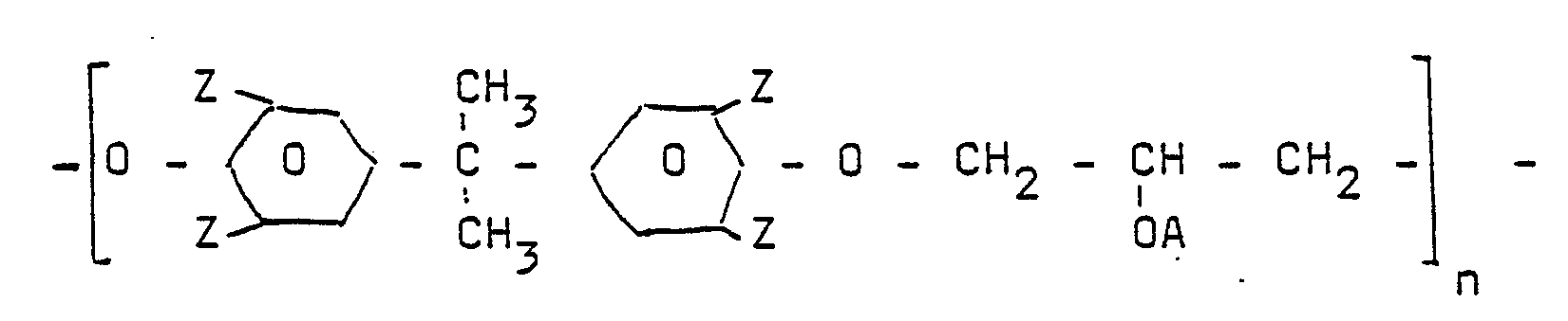
A der Acylrest einer Acrylsäure, vorzugsweise Zimtsäure oder Furanacrylsäure und n eine ganze Zahl bedeutet. Dabei ist n so gewählt, daß die mittlere Molmasse des Polymeren ca. 10.000 Gramm/mol beträgt. Als Nebenkomponente B werden Polyetherpolyacrylate der allgemeinen Strukturen (1), (2) und (3) zugesetzt. - Die aus diesem Polymersystem durch UV-Härtung erhaltenen Harze zeigen ausreichend hohe Glasübergangstemperaturen und niedrige Dielektrizitätskonstanten (kleiner gleich 3,1). Auch gegenüber thermischer Dauerbelastung bei Temperaturen von über 100°C zeigen diese Harze eine hervorragende Beständigkeit und sind daher bestens zur Herstellung von Mikroverdrahtungen geeignet.
- In einem Ausführungsbeispiel wird im folgenden die Darstellung eines erfindungsgemäßen Polymersystems beschrieben und anhand der Figuren 1 und 2 die Anwendung des Polymersystems bei der Herstellung einer Mehrlagenverdrahtung beschrieben. Dabei zeigen
die Figuren 1 und 2 im Schnittbild die wesentlichsten Verfahrensschritte. - Zur Darstellung eines der allgemeinen Struktur (1) entsprechenden Acrylats wird vom entsprechenden Trisepoxid (5) ausgegangen.

- Das bei Raumtemperatur feste Trisepoxid (5) wird in der vierfachen Menge Toluol p.a. gelöst. Dazu gibt man über Nacht bei 50°C über einem Trockenmittel vorgetrocknetes Zimtsäurechlorid in etwa 15 % Überschuß zur Stöchiometrie (entspricht 0,46 Massenteile bezogen auf Epoxid). Darauf wird die Mischung ca. 20 Stunden unter Rückfluß gekocht, wobei sich die Komponenten miteinander umsetzen. Das Rohprodukt wird durch Eingießen in die fünffache Menge Methanol p.a. ausgefällt und nach Abtrennen vom Lösungsmittel bei 50°C im Vakuum getrocknet. Gegebenenfalls wird das Ausfällen zum Erzielen eines höheren Reinheitsgrades wiederholt.
- Das trockene Produkt wird dann zusammen mit 5 Gewichtsprozent Pentaerythritoltetraacrylat in einer der Weiterverarbeitung entsprechenden Menge Toluol gelöst. Man erhält das erfindungsgemäße Polymersystem.
- Figur 1: Als Träger der zukünftigen Mikroverdrahtung wird eine Kupferfolie 1 verwendet, auf die eine Schicht 2 des strahlungsvernetzbaren Polymersystems (nach Zusatz von zum Beispiel Michlers Keton als Sensibilisator) durch Tauchen oder Sprühbelacken, beispielsweise in einer Schichtdicke von 5 bis 20 µm aufgebracht wird. Die Schicht 2 wird in der Weise belichtet und entwickelt, daß die in ihr einzufügenden Durchkontaktierungen, das heißt die Anschlußpunkte der Chips als Durchbrechungen 3 in der Isolierstoffschicht 2 entstehen. Die Bestrahlung der Schicht erfolgt dabei unter Verwendung einer Maske (nicht abgebildet), die den Bereich der Durchbrechungen 3 der Schicht 2 abdeckt (Negativlack). Die abgedeckten Teile 3 werden anschließend mit einem entsprechenden Lösungsmittel herausgelöst, während bei den belichteten Teilen 13 der Schicht 2 eine chemische Vernetzung eingetreten ist, die eine Lösung verhindert, so daß diese Teile 13 als Isolierstoffschicht verbleiben. Nach der Herstellung der Durchbrechungen 3 für die dieser ersten Isolierstoffschicht 2 (13) zugeordneten Durchkontaktierungen werden die Durchbrechungen 3 im Zusammenhang mit der als Träger dienenden Kupferfolie 1 mittels galvanischer Metallisierung mit einem elektrisch gut leitenden Material, beispielsweise Kupfer, ausgefüllt (23 in Figur 2).
- Figur 2: Anschließend wird auf die die Durchkontaktierungen 23 enthaltende Isolierstoffschicht 13 eine weitere Schicht 4 des photovernetzbaren Isolierstoffes nach der Lehre der Erfindung in der gleichen Weise wie bei Figur 1 beschrieben, aufgebracht, in welche Leitungsbahnen 5 und weitere Durchkontaktierungen 6 eingefügt werden. Die Belichtung und Entwicklung der Schicht 4 erfolgt ebenfalls wie bei Figur 1 beschrieben. Außer den Durchbrechungen 6 für die Durchkontaktierung, die mit den Durchkontaktierungen 3 der ersten Isolierstoffschicht 2 (13) zur Auflage kommen, werden in der zweiten Isolierstoffschicht 4 grabenförmige Aussparungen 5 für die gewünschten Leitungsbahnen erzeugt, wobei diese Aussparungen 5 so angeordnet sind, daß min destens eine Durchkontaktierung 23 der ersten Isolierstoffschicht (2, 13) in eine Aussparung 5 hineinragt. Zum Aufbau der Leitungsbahnen werden die Aussparungen 5 durch Galvanisieren mit einer Metallisierung versehen. Weitere Durchkontaktierungen und Leiterbahnen können dann durch entsprechende Wiederholung der vorstehend beschriebenen Herstellungsstufen aufgebracht werden.
- Der neuartige Verdrahtungsaufbau hat gegenüber bekannten Systemen nicht nur den Vorteil einer wesentlich kürzeren Belichtungszeit, sondern erfordert auch keine Zwischen- oder Endtemperungen, durch welche Zersetzungsprodukte entstehen können, die die Struktur verändern. Ebenso erübrigt sich die Verwendung von weiteren Passivierungsschichten. Dadurch vereinfacht sich nicht nur das Verfahren zur Herstellung eines solchen Aufbaus, sondern auch die Zuverlässigkeit in bezug auf die elektrischen Daten.

Claims (12)

und wobei A den Acylrest einer substituierten Acrylsäure darstellt.


Applications Claiming Priority (2)
| Application Number | Priority Date | Filing Date | Title |
|---|---|---|---|
| DE3708057 | 1987-03-12 | ||
| DE3708057 | 1987-03-12 |
Publications (3)
| Publication Number | Publication Date |
|---|---|
| EP0281808A2 true EP0281808A2 (de) | 1988-09-14 |
| EP0281808A3 EP0281808A3 (en) | 1990-05-16 |
| EP0281808B1 EP0281808B1 (de) | 1994-07-20 |
Family
ID=6322925
Family Applications (1)
| Application Number | Title | Priority Date | Filing Date |
|---|---|---|---|
| EP88102309A Expired - Lifetime EP0281808B1 (de) | 1987-03-12 | 1988-02-17 | Strahlungsvernetzbares Polymersystem zur Anwendung als Photoresist und Dielektrikum für Mikroverdrahtungen |
Country Status (4)
| Country | Link |
|---|---|
| EP (1) | EP0281808B1 (de) |
| JP (1) | JPS63243120A (de) |
| AT (1) | ATE108914T1 (de) |
| DE (1) | DE3850689D1 (de) |
Cited By (9)
| Publication number | Priority date | Publication date | Assignee | Title |
|---|---|---|---|---|
| EP0827027A2 (de) * | 1996-08-29 | 1998-03-04 | Xerox Corporation | Härtbare Zusammensetzungen |
| EP0827030A2 (de) * | 1996-08-29 | 1998-03-04 | Xerox Corporation | Verfahren zur direkten Substitution von Hochleistung-Polymeren mit ungesättigten Estergruppen |
| US5945253A (en) * | 1996-08-29 | 1999-08-31 | Xerox Corporation | High performance curable polymers and processes for the preparation thereof |
| US5958995A (en) * | 1996-08-29 | 1999-09-28 | Xerox Corporation | Blends containing photosensitive high performance aromatic ether curable polymers |
| US6117967A (en) * | 1999-06-04 | 2000-09-12 | Xerox Corporation | Arylene ether alcohol polymers |
| US6124372A (en) * | 1996-08-29 | 2000-09-26 | Xerox Corporation | High performance polymer compositions having photosensitivity-imparting substituents and thermal sensitivity-imparting substituents |
| US6139920A (en) * | 1998-12-21 | 2000-10-31 | Xerox Corporation | Photoresist compositions |
| US6174636B1 (en) | 1999-06-04 | 2001-01-16 | Xerox Corporation | Imaging members containing arylene ether alcohol polymers |
| US6177238B1 (en) | 1999-06-04 | 2001-01-23 | Xerox Corporation | Ink jet printheads containing arylene ether alcohol polymers and processes for their formation |
Citations (6)
| Publication number | Priority date | Publication date | Assignee | Title |
|---|---|---|---|---|
| US3738973A (en) * | 1971-01-07 | 1973-06-12 | Powers Chemco Inc | Furoic acid esters of hydroxycontaining polymers |
| FR2259863A1 (en) * | 1974-02-01 | 1975-08-29 | Oce Van Der Grinten Nv | Photo-sensitive polymers for lithographic plates, etc. - consisting of 3-(2-furyl) acrylic acid esters of phenoxy resins |
| FR2440978A1 (fr) * | 1978-11-01 | 1980-06-06 | Coates Brothers & Co | Compositions de revetement et procede de formation d'un revetement a partir de ladite composition |
| EP0167051A1 (de) * | 1984-06-29 | 1986-01-08 | Siemens Aktiengesellschaft | Thermostabiles, durch Bestrahlung vernetzbares Polymersystem auf der Basis von Bisphenolen und Epichlorhydrin sowie Verfahren zu seiner Verwendung |
| EP0174494A2 (de) * | 1984-08-10 | 1986-03-19 | Siemens Aktiengesellschaft | Thermostabiles, durch Bestrahlung vernetzbares Polymersystem für mikroelektronische Anwendung |
| EP0204292A2 (de) * | 1985-06-05 | 1986-12-10 | Siemens Aktiengesellschaft | Verfahren zum Herstellen von gedruckten Schaltungen unter Verwendung eines durch Strahlung vernetzenden Fotopolymersystems |
-
1988
- 1988-02-17 AT AT88102309T patent/ATE108914T1/de not_active IP Right Cessation
- 1988-02-17 DE DE3850689T patent/DE3850689D1/de not_active Expired - Fee Related
- 1988-02-17 EP EP88102309A patent/EP0281808B1/de not_active Expired - Lifetime
- 1988-03-09 JP JP63057321A patent/JPS63243120A/ja active Pending
Patent Citations (6)
| Publication number | Priority date | Publication date | Assignee | Title |
|---|---|---|---|---|
| US3738973A (en) * | 1971-01-07 | 1973-06-12 | Powers Chemco Inc | Furoic acid esters of hydroxycontaining polymers |
| FR2259863A1 (en) * | 1974-02-01 | 1975-08-29 | Oce Van Der Grinten Nv | Photo-sensitive polymers for lithographic plates, etc. - consisting of 3-(2-furyl) acrylic acid esters of phenoxy resins |
| FR2440978A1 (fr) * | 1978-11-01 | 1980-06-06 | Coates Brothers & Co | Compositions de revetement et procede de formation d'un revetement a partir de ladite composition |
| EP0167051A1 (de) * | 1984-06-29 | 1986-01-08 | Siemens Aktiengesellschaft | Thermostabiles, durch Bestrahlung vernetzbares Polymersystem auf der Basis von Bisphenolen und Epichlorhydrin sowie Verfahren zu seiner Verwendung |
| EP0174494A2 (de) * | 1984-08-10 | 1986-03-19 | Siemens Aktiengesellschaft | Thermostabiles, durch Bestrahlung vernetzbares Polymersystem für mikroelektronische Anwendung |
| EP0204292A2 (de) * | 1985-06-05 | 1986-12-10 | Siemens Aktiengesellschaft | Verfahren zum Herstellen von gedruckten Schaltungen unter Verwendung eines durch Strahlung vernetzenden Fotopolymersystems |
Cited By (23)
| Publication number | Priority date | Publication date | Assignee | Title |
|---|---|---|---|---|
| US6124372A (en) * | 1996-08-29 | 2000-09-26 | Xerox Corporation | High performance polymer compositions having photosensitivity-imparting substituents and thermal sensitivity-imparting substituents |
| US7517641B2 (en) | 1996-08-29 | 2009-04-14 | Xerox Corporation | High performance curable polymers and processes for the preparation thereof |
| EP0827027A2 (de) * | 1996-08-29 | 1998-03-04 | Xerox Corporation | Härtbare Zusammensetzungen |
| EP0827027A3 (de) * | 1996-08-29 | 1998-06-17 | Xerox Corporation | Härtbare Zusammensetzungen |
| US5889077A (en) * | 1996-08-29 | 1999-03-30 | Xerox Corporation | Process for direct substitution of high performance polymers with unsaturated ester groups |
| US5945253A (en) * | 1996-08-29 | 1999-08-31 | Xerox Corporation | High performance curable polymers and processes for the preparation thereof |
| US5958995A (en) * | 1996-08-29 | 1999-09-28 | Xerox Corporation | Blends containing photosensitive high performance aromatic ether curable polymers |
| US5994425A (en) * | 1996-08-29 | 1999-11-30 | Xerox Corporation | Curable compositions containing photosensitive high performance aromatic ether polymers |
| US6087414A (en) * | 1996-08-29 | 2000-07-11 | Xerox Corporation | Process for direct substitution of high performance polymers with unsaturated ester groups |
| US6151042A (en) * | 1996-08-29 | 2000-11-21 | Xerox Corporation | High performance polymer compositions |
| EP0827030A3 (de) * | 1996-08-29 | 1998-06-17 | Xerox Corporation | Verfahren zur direkten Substitution von Hochleistung-Polymeren mit ungesättigten Estergruppen |
| EP0827030A2 (de) * | 1996-08-29 | 1998-03-04 | Xerox Corporation | Verfahren zur direkten Substitution von Hochleistung-Polymeren mit ungesättigten Estergruppen |
| US7252927B2 (en) | 1996-08-29 | 2007-08-07 | Xerox Corporation | High performance curable polymers and processes for the preparation thereof |
| US6897267B2 (en) | 1996-08-29 | 2005-05-24 | Xerox Corporation | High performance curable polymers and processes for the preparation thereof |
| EP1219660A3 (de) * | 1996-08-29 | 2003-11-26 | Xerox Corporation | Verfahren zur direkten Substitution von Hochleistungspolymeren mit ungesättigten Estergruppen |
| US6184263B1 (en) | 1996-08-29 | 2001-02-06 | Xerox Corporation | Blends containing photosensitive high performance aromatic ether curable polymers |
| US6323301B1 (en) | 1996-08-29 | 2001-11-27 | Xerox Corporation | High performance UV and heat crosslinked or chain extended polymers |
| US6365323B1 (en) | 1996-08-29 | 2002-04-02 | Xerox Corporation | High performance curable polymers and processes for the preparation thereof |
| EP1219660A2 (de) * | 1996-08-29 | 2002-07-03 | Xerox Corporation | Verfahren zur direkten Substitution von Hochleistungspolymeren mit ungesättigten Estergruppen |
| US6139920A (en) * | 1998-12-21 | 2000-10-31 | Xerox Corporation | Photoresist compositions |
| US6177238B1 (en) | 1999-06-04 | 2001-01-23 | Xerox Corporation | Ink jet printheads containing arylene ether alcohol polymers and processes for their formation |
| US6174636B1 (en) | 1999-06-04 | 2001-01-16 | Xerox Corporation | Imaging members containing arylene ether alcohol polymers |
| US6117967A (en) * | 1999-06-04 | 2000-09-12 | Xerox Corporation | Arylene ether alcohol polymers |
Also Published As
| Publication number | Publication date |
|---|---|
| EP0281808B1 (de) | 1994-07-20 |
| DE3850689D1 (de) | 1994-08-25 |
| EP0281808A3 (en) | 1990-05-16 |
| ATE108914T1 (de) | 1994-08-15 |
| JPS63243120A (ja) | 1988-10-11 |
Similar Documents
| Publication | Publication Date | Title |
|---|---|---|
| DE69937561T2 (de) | Photolithographisch hergestellter, integrierter kondensator mit selbst-ausgerichteten elektroden und dielektrika | |
| DE3687409T2 (de) | Verfahren zur herstellung von schmalen, leitenden linien, von mustern und von verbindern. | |
| EP0167051B1 (de) | Thermostabiles, durch Bestrahlung vernetzbares Polymersystem auf der Basis von Bisphenolen und Epichlorhydrin sowie Verfahren zu seiner Verwendung | |
| EP0101587B1 (de) | Positiv arbeitendes Verfahren zur Herstellung von Reliefbildern oder Resistmustern | |
| DE2342407C3 (de) | Verfahren zur Herstellung von gedruckten Mehrlagen-Schaltungen | |
| EP0008359A2 (de) | Verfahren zum Herstellen einer Dünnfilmstruktur | |
| DE2326314C2 (de) | Verfahren zur Herstellung von Reliefstrukturen | |
| DE3545989C2 (de) | ||
| DE1817434C3 (de) | Verfahren zur Herstellung einer elektrischen Leitungsanordnung | |
| EP0174494B1 (de) | Thermostabiles, durch Bestrahlung vernetzbares Polymersystem für mikroelektronische Anwendung | |
| EP0281808B1 (de) | Strahlungsvernetzbares Polymersystem zur Anwendung als Photoresist und Dielektrikum für Mikroverdrahtungen | |
| EP0549791B1 (de) | Mehrlagenleiterplatte und verfahren zu ihrer herstellung | |
| EP0157930B1 (de) | Verfahren zur Herstellung von Polyimid- und Polyisoindolochinazolindion-Reliefstrukturen | |
| EP0206159B1 (de) | Verfahren zur Herstellung wärmebeständiger strukturierter Schichten und deren Verwendung | |
| EP0259727A2 (de) | Verfahren zur Herstellung wärmebeständiger strukturierter Schichten auf Epoxidharzbasis | |
| EP0259723B1 (de) | Verfahren zur Herstellung wärmebeständiger strukturierter Schichten | |
| DE2618937B2 (de) | Ätzmittel für Polymerisatharze, insbesondere für die Halbleiterherstellung, und Verfahren zur Herstellung von Halbleiterbauelementen unter Verwendung dieses Ätzmittels | |
| EP0013728A1 (de) | Verfahren zur Herstellung von elektrischen Verbindungen zwischen Leiterschichten in Halbleiterstrukturen | |
| DE68915642T2 (de) | Für hochenergetische Strahlung empfindliches Copolymer. | |
| DE2514139A1 (de) | Verfahren zum herstellen eines kondensators | |
| EP0157932A1 (de) | Verfahren zur Herstellung von Polyimidazol- und Polyimidazopyrrolon-Reliefstrukturen | |
| EP0204292B1 (de) | Verfahren zum Herstellen von gedruckten Schaltungen unter Verwendung eines durch Strahlung vernetzenden Fotopolymersystems | |
| EP1238311B1 (de) | Flachspule und lithographisches verfahren zur herstellung von mikrobauteilen | |
| DE69414027T2 (de) | Resistzusammensetzungen für gedruckte Schaltungen | |
| DE69701952T2 (de) | Isolationsschicht und Verfahren zu ihrer Herstellung |
Legal Events
| Date | Code | Title | Description |
|---|---|---|---|
| PUAI | Public reference made under article 153(3) epc to a published international application that has entered the european phase |
Free format text: ORIGINAL CODE: 0009012 |
|
| AK | Designated contracting states |
Kind code of ref document: A2 Designated state(s): AT BE CH DE FR GB IT LI LU NL SE |
|
| PUAL | Search report despatched |
Free format text: ORIGINAL CODE: 0009013 |
|
| AK | Designated contracting states |
Kind code of ref document: A3 Designated state(s): AT BE CH DE FR GB IT LI LU NL SE |
|
| 17P | Request for examination filed |
Effective date: 19901113 |
|
| 17Q | First examination report despatched |
Effective date: 19930319 |
|
| GRAA | (expected) grant |
Free format text: ORIGINAL CODE: 0009210 |
|
| AK | Designated contracting states |
Kind code of ref document: B1 Designated state(s): AT BE CH DE FR GB IT LI LU NL SE |
|
| REF | Corresponds to: |
Ref document number: 108914 Country of ref document: AT Date of ref document: 19940815 Kind code of ref document: T |
|
| REF | Corresponds to: |
Ref document number: 3850689 Country of ref document: DE Date of ref document: 19940825 |
|
| ITF | It: translation for a ep patent filed | ||
| GBT | Gb: translation of ep patent filed (gb section 77(6)(a)/1977) |
Effective date: 19940926 |
|
| ET | Fr: translation filed | ||
| EAL | Se: european patent in force in sweden |
Ref document number: 88102309.7 |
|
| PGFP | Annual fee paid to national office [announced via postgrant information from national office to epo] |
Ref country code: LU Payment date: 19950201 Year of fee payment: 8 |
|
| PLBE | No opposition filed within time limit |
Free format text: ORIGINAL CODE: 0009261 |
|
| STAA | Information on the status of an ep patent application or granted ep patent |
Free format text: STATUS: NO OPPOSITION FILED WITHIN TIME LIMIT |
|
| 26N | No opposition filed | ||
| PGFP | Annual fee paid to national office [announced via postgrant information from national office to epo] |
Ref country code: GB Payment date: 19960122 Year of fee payment: 9 |
|
| PGFP | Annual fee paid to national office [announced via postgrant information from national office to epo] |
Ref country code: AT Payment date: 19960124 Year of fee payment: 9 |
|
| PGFP | Annual fee paid to national office [announced via postgrant information from national office to epo] |
Ref country code: NL Payment date: 19960215 Year of fee payment: 9 |
|
| PGFP | Annual fee paid to national office [announced via postgrant information from national office to epo] |
Ref country code: BE Payment date: 19960216 Year of fee payment: 9 |
|
| PG25 | Lapsed in a contracting state [announced via postgrant information from national office to epo] |
Ref country code: LU Free format text: LAPSE BECAUSE OF NON-PAYMENT OF DUE FEES Effective date: 19960217 |
|
| PGFP | Annual fee paid to national office [announced via postgrant information from national office to epo] |
Ref country code: FR Payment date: 19960221 Year of fee payment: 9 |
|
| PGFP | Annual fee paid to national office [announced via postgrant information from national office to epo] |
Ref country code: SE Payment date: 19960222 Year of fee payment: 9 |
|
| PGFP | Annual fee paid to national office [announced via postgrant information from national office to epo] |
Ref country code: DE Payment date: 19960419 Year of fee payment: 9 |
|
| PGFP | Annual fee paid to national office [announced via postgrant information from national office to epo] |
Ref country code: CH Payment date: 19960520 Year of fee payment: 9 |
|
| PG25 | Lapsed in a contracting state [announced via postgrant information from national office to epo] |
Ref country code: GB Effective date: 19970217 Ref country code: AT Effective date: 19970217 |
|
| PG25 | Lapsed in a contracting state [announced via postgrant information from national office to epo] |
Ref country code: SE Effective date: 19970218 |
|
| PG25 | Lapsed in a contracting state [announced via postgrant information from national office to epo] |
Ref country code: LI Effective date: 19970228 Ref country code: CH Effective date: 19970228 Ref country code: BE Effective date: 19970228 |
|
| BERE | Be: lapsed |
Owner name: SIEMENS A.G. Effective date: 19970228 |
|
| PG25 | Lapsed in a contracting state [announced via postgrant information from national office to epo] |
Ref country code: NL Effective date: 19970901 |
|
| GBPC | Gb: european patent ceased through non-payment of renewal fee |
Effective date: 19970217 |
|
| REG | Reference to a national code |
Ref country code: CH Ref legal event code: PL |
|
| PG25 | Lapsed in a contracting state [announced via postgrant information from national office to epo] |
Ref country code: FR Effective date: 19971030 |
|
| PG25 | Lapsed in a contracting state [announced via postgrant information from national office to epo] |
Ref country code: DE Effective date: 19971101 |
|
| EUG | Se: european patent has lapsed |
Ref document number: 88102309.7 |
|
| NLV4 | Nl: lapsed or anulled due to non-payment of the annual fee |
Effective date: 19970901 |
|
| REG | Reference to a national code |
Ref country code: FR Ref legal event code: ST |
|
| PG25 | Lapsed in a contracting state [announced via postgrant information from national office to epo] |
Ref country code: IT Free format text: LAPSE BECAUSE OF NON-PAYMENT OF DUE FEES;WARNING: LAPSES OF ITALIAN PATENTS WITH EFFECTIVE DATE BEFORE 2007 MAY HAVE OCCURRED AT ANY TIME BEFORE 2007. THE CORRECT EFFECTIVE DATE MAY BE DIFFERENT FROM THE ONE RECORDED. Effective date: 20050217 |