EP0280235A2 - Dreiphasiger Umformermodul mit Brückenschaltung - Google Patents
Dreiphasiger Umformermodul mit Brückenschaltung Download PDFInfo
- Publication number
- EP0280235A2 EP0280235A2 EP19880102573 EP88102573A EP0280235A2 EP 0280235 A2 EP0280235 A2 EP 0280235A2 EP 19880102573 EP19880102573 EP 19880102573 EP 88102573 A EP88102573 A EP 88102573A EP 0280235 A2 EP0280235 A2 EP 0280235A2
- Authority
- EP
- European Patent Office
- Prior art keywords
- lead
- switching means
- terminal
- bonding wire
- control input
- Prior art date
- Legal status (The legal status is an assumption and is not a legal conclusion. Google has not performed a legal analysis and makes no representation as to the accuracy of the status listed.)
- Withdrawn
Links
Images

Classifications
-
- H—ELECTRICITY
- H02—GENERATION; CONVERSION OR DISTRIBUTION OF ELECTRIC POWER
- H02M—APPARATUS FOR CONVERSION BETWEEN AC AND AC, BETWEEN AC AND DC, OR BETWEEN DC AND DC, AND FOR USE WITH MAINS OR SIMILAR POWER SUPPLY SYSTEMS; CONVERSION OF DC OR AC INPUT POWER INTO SURGE OUTPUT POWER; CONTROL OR REGULATION THEREOF
- H02M7/00—Conversion of ac power input into dc power output; Conversion of dc power input into ac power output
- H02M7/42—Conversion of dc power input into ac power output without possibility of reversal
- H02M7/44—Conversion of dc power input into ac power output without possibility of reversal by static converters
- H02M7/48—Conversion of dc power input into ac power output without possibility of reversal by static converters using discharge tubes with control electrode or semiconductor devices with control electrode
-
- H—ELECTRICITY
- H01—ELECTRIC ELEMENTS
- H01L—SEMICONDUCTOR DEVICES NOT COVERED BY CLASS H10
- H01L24/00—Arrangements for connecting or disconnecting semiconductor or solid-state bodies; Methods or apparatus related thereto
- H01L24/01—Means for bonding being attached to, or being formed on, the surface to be connected, e.g. chip-to-package, die-attach, "first-level" interconnects; Manufacturing methods related thereto
- H01L24/42—Wire connectors; Manufacturing methods related thereto
- H01L24/47—Structure, shape, material or disposition of the wire connectors after the connecting process
- H01L24/49—Structure, shape, material or disposition of the wire connectors after the connecting process of a plurality of wire connectors
-
- H—ELECTRICITY
- H01—ELECTRIC ELEMENTS
- H01L—SEMICONDUCTOR DEVICES NOT COVERED BY CLASS H10
- H01L23/00—Details of semiconductor or other solid state devices
- H01L23/48—Arrangements for conducting electric current to or from the solid state body in operation, e.g. leads, terminal arrangements ; Selection of materials therefor
- H01L23/488—Arrangements for conducting electric current to or from the solid state body in operation, e.g. leads, terminal arrangements ; Selection of materials therefor consisting of soldered or bonded constructions
- H01L23/495—Lead-frames or other flat leads
- H01L23/49575—Assemblies of semiconductor devices on lead frames
-
- H—ELECTRICITY
- H01—ELECTRIC ELEMENTS
- H01L—SEMICONDUCTOR DEVICES NOT COVERED BY CLASS H10
- H01L25/00—Assemblies consisting of a plurality of individual semiconductor or other solid state devices ; Multistep manufacturing processes thereof
- H01L25/03—Assemblies consisting of a plurality of individual semiconductor or other solid state devices ; Multistep manufacturing processes thereof all the devices being of a type provided for in the same subgroup of groups H01L27/00 - H01L33/00, or in a single subclass of H10K, H10N, e.g. assemblies of rectifier diodes
- H01L25/04—Assemblies consisting of a plurality of individual semiconductor or other solid state devices ; Multistep manufacturing processes thereof all the devices being of a type provided for in the same subgroup of groups H01L27/00 - H01L33/00, or in a single subclass of H10K, H10N, e.g. assemblies of rectifier diodes the devices not having separate containers
- H01L25/07—Assemblies consisting of a plurality of individual semiconductor or other solid state devices ; Multistep manufacturing processes thereof all the devices being of a type provided for in the same subgroup of groups H01L27/00 - H01L33/00, or in a single subclass of H10K, H10N, e.g. assemblies of rectifier diodes the devices not having separate containers the devices being of a type provided for in group H01L29/00
- H01L25/072—Assemblies consisting of a plurality of individual semiconductor or other solid state devices ; Multistep manufacturing processes thereof all the devices being of a type provided for in the same subgroup of groups H01L27/00 - H01L33/00, or in a single subclass of H10K, H10N, e.g. assemblies of rectifier diodes the devices not having separate containers the devices being of a type provided for in group H01L29/00 the devices being arranged next to each other
-
- H—ELECTRICITY
- H02—GENERATION; CONVERSION OR DISTRIBUTION OF ELECTRIC POWER
- H02M—APPARATUS FOR CONVERSION BETWEEN AC AND AC, BETWEEN AC AND DC, OR BETWEEN DC AND DC, AND FOR USE WITH MAINS OR SIMILAR POWER SUPPLY SYSTEMS; CONVERSION OF DC OR AC INPUT POWER INTO SURGE OUTPUT POWER; CONTROL OR REGULATION THEREOF
- H02M7/00—Conversion of ac power input into dc power output; Conversion of dc power input into ac power output
- H02M7/003—Constructional details, e.g. physical layout, assembly, wiring or busbar connections
-
- H—ELECTRICITY
- H02—GENERATION; CONVERSION OR DISTRIBUTION OF ELECTRIC POWER
- H02M—APPARATUS FOR CONVERSION BETWEEN AC AND AC, BETWEEN AC AND DC, OR BETWEEN DC AND DC, AND FOR USE WITH MAINS OR SIMILAR POWER SUPPLY SYSTEMS; CONVERSION OF DC OR AC INPUT POWER INTO SURGE OUTPUT POWER; CONTROL OR REGULATION THEREOF
- H02M7/00—Conversion of ac power input into dc power output; Conversion of dc power input into ac power output
- H02M7/42—Conversion of dc power input into ac power output without possibility of reversal
- H02M7/44—Conversion of dc power input into ac power output without possibility of reversal by static converters
- H02M7/48—Conversion of dc power input into ac power output without possibility of reversal by static converters using discharge tubes with control electrode or semiconductor devices with control electrode
- H02M7/53—Conversion of dc power input into ac power output without possibility of reversal by static converters using discharge tubes with control electrode or semiconductor devices with control electrode using devices of a triode or transistor type requiring continuous application of a control signal
- H02M7/537—Conversion of dc power input into ac power output without possibility of reversal by static converters using discharge tubes with control electrode or semiconductor devices with control electrode using devices of a triode or transistor type requiring continuous application of a control signal using semiconductor devices only, e.g. single switched pulse inverters
- H02M7/5387—Conversion of dc power input into ac power output without possibility of reversal by static converters using discharge tubes with control electrode or semiconductor devices with control electrode using devices of a triode or transistor type requiring continuous application of a control signal using semiconductor devices only, e.g. single switched pulse inverters in a bridge configuration
-
- H—ELECTRICITY
- H01—ELECTRIC ELEMENTS
- H01L—SEMICONDUCTOR DEVICES NOT COVERED BY CLASS H10
- H01L2224/00—Indexing scheme for arrangements for connecting or disconnecting semiconductor or solid-state bodies and methods related thereto as covered by H01L24/00
- H01L2224/01—Means for bonding being attached to, or being formed on, the surface to be connected, e.g. chip-to-package, die-attach, "first-level" interconnects; Manufacturing methods related thereto
- H01L2224/42—Wire connectors; Manufacturing methods related thereto
- H01L2224/44—Structure, shape, material or disposition of the wire connectors prior to the connecting process
- H01L2224/45—Structure, shape, material or disposition of the wire connectors prior to the connecting process of an individual wire connector
- H01L2224/45001—Core members of the connector
- H01L2224/45099—Material
- H01L2224/451—Material with a principal constituent of the material being a metal or a metalloid, e.g. boron (B), silicon (Si), germanium (Ge), arsenic (As), antimony (Sb), tellurium (Te) and polonium (Po), and alloys thereof
- H01L2224/45117—Material with a principal constituent of the material being a metal or a metalloid, e.g. boron (B), silicon (Si), germanium (Ge), arsenic (As), antimony (Sb), tellurium (Te) and polonium (Po), and alloys thereof the principal constituent melting at a temperature of greater than or equal to 400°C and less than 950°C
- H01L2224/45124—Aluminium (Al) as principal constituent
-
- H—ELECTRICITY
- H01—ELECTRIC ELEMENTS
- H01L—SEMICONDUCTOR DEVICES NOT COVERED BY CLASS H10
- H01L2224/00—Indexing scheme for arrangements for connecting or disconnecting semiconductor or solid-state bodies and methods related thereto as covered by H01L24/00
- H01L2224/01—Means for bonding being attached to, or being formed on, the surface to be connected, e.g. chip-to-package, die-attach, "first-level" interconnects; Manufacturing methods related thereto
- H01L2224/42—Wire connectors; Manufacturing methods related thereto
- H01L2224/47—Structure, shape, material or disposition of the wire connectors after the connecting process
- H01L2224/48—Structure, shape, material or disposition of the wire connectors after the connecting process of an individual wire connector
- H01L2224/481—Disposition
- H01L2224/48151—Connecting between a semiconductor or solid-state body and an item not being a semiconductor or solid-state body, e.g. chip-to-substrate, chip-to-passive
- H01L2224/48221—Connecting between a semiconductor or solid-state body and an item not being a semiconductor or solid-state body, e.g. chip-to-substrate, chip-to-passive the body and the item being stacked
- H01L2224/48245—Connecting between a semiconductor or solid-state body and an item not being a semiconductor or solid-state body, e.g. chip-to-substrate, chip-to-passive the body and the item being stacked the item being metallic
- H01L2224/48247—Connecting between a semiconductor or solid-state body and an item not being a semiconductor or solid-state body, e.g. chip-to-substrate, chip-to-passive the body and the item being stacked the item being metallic connecting the wire to a bond pad of the item
-
- H—ELECTRICITY
- H01—ELECTRIC ELEMENTS
- H01L—SEMICONDUCTOR DEVICES NOT COVERED BY CLASS H10
- H01L2224/00—Indexing scheme for arrangements for connecting or disconnecting semiconductor or solid-state bodies and methods related thereto as covered by H01L24/00
- H01L2224/01—Means for bonding being attached to, or being formed on, the surface to be connected, e.g. chip-to-package, die-attach, "first-level" interconnects; Manufacturing methods related thereto
- H01L2224/42—Wire connectors; Manufacturing methods related thereto
- H01L2224/47—Structure, shape, material or disposition of the wire connectors after the connecting process
- H01L2224/49—Structure, shape, material or disposition of the wire connectors after the connecting process of a plurality of wire connectors
- H01L2224/491—Disposition
- H01L2224/4912—Layout
- H01L2224/49171—Fan-out arrangements
-
- H—ELECTRICITY
- H01—ELECTRIC ELEMENTS
- H01L—SEMICONDUCTOR DEVICES NOT COVERED BY CLASS H10
- H01L24/00—Arrangements for connecting or disconnecting semiconductor or solid-state bodies; Methods or apparatus related thereto
- H01L24/01—Means for bonding being attached to, or being formed on, the surface to be connected, e.g. chip-to-package, die-attach, "first-level" interconnects; Manufacturing methods related thereto
- H01L24/42—Wire connectors; Manufacturing methods related thereto
- H01L24/44—Structure, shape, material or disposition of the wire connectors prior to the connecting process
- H01L24/45—Structure, shape, material or disposition of the wire connectors prior to the connecting process of an individual wire connector
-
- H—ELECTRICITY
- H01—ELECTRIC ELEMENTS
- H01L—SEMICONDUCTOR DEVICES NOT COVERED BY CLASS H10
- H01L24/00—Arrangements for connecting or disconnecting semiconductor or solid-state bodies; Methods or apparatus related thereto
- H01L24/01—Means for bonding being attached to, or being formed on, the surface to be connected, e.g. chip-to-package, die-attach, "first-level" interconnects; Manufacturing methods related thereto
- H01L24/42—Wire connectors; Manufacturing methods related thereto
- H01L24/47—Structure, shape, material or disposition of the wire connectors after the connecting process
- H01L24/48—Structure, shape, material or disposition of the wire connectors after the connecting process of an individual wire connector
-
- H—ELECTRICITY
- H01—ELECTRIC ELEMENTS
- H01L—SEMICONDUCTOR DEVICES NOT COVERED BY CLASS H10
- H01L2924/00—Indexing scheme for arrangements or methods for connecting or disconnecting semiconductor or solid-state bodies as covered by H01L24/00
- H01L2924/0001—Technical content checked by a classifier
- H01L2924/00014—Technical content checked by a classifier the subject-matter covered by the group, the symbol of which is combined with the symbol of this group, being disclosed without further technical details
-
- H—ELECTRICITY
- H01—ELECTRIC ELEMENTS
- H01L—SEMICONDUCTOR DEVICES NOT COVERED BY CLASS H10
- H01L2924/00—Indexing scheme for arrangements or methods for connecting or disconnecting semiconductor or solid-state bodies as covered by H01L24/00
- H01L2924/01—Chemical elements
- H01L2924/01006—Carbon [C]
-
- H—ELECTRICITY
- H01—ELECTRIC ELEMENTS
- H01L—SEMICONDUCTOR DEVICES NOT COVERED BY CLASS H10
- H01L2924/00—Indexing scheme for arrangements or methods for connecting or disconnecting semiconductor or solid-state bodies as covered by H01L24/00
- H01L2924/01—Chemical elements
- H01L2924/01013—Aluminum [Al]
-
- H—ELECTRICITY
- H01—ELECTRIC ELEMENTS
- H01L—SEMICONDUCTOR DEVICES NOT COVERED BY CLASS H10
- H01L2924/00—Indexing scheme for arrangements or methods for connecting or disconnecting semiconductor or solid-state bodies as covered by H01L24/00
- H01L2924/01—Chemical elements
- H01L2924/01015—Phosphorus [P]
-
- H—ELECTRICITY
- H01—ELECTRIC ELEMENTS
- H01L—SEMICONDUCTOR DEVICES NOT COVERED BY CLASS H10
- H01L2924/00—Indexing scheme for arrangements or methods for connecting or disconnecting semiconductor or solid-state bodies as covered by H01L24/00
- H01L2924/01—Chemical elements
- H01L2924/01023—Vanadium [V]
-
- H—ELECTRICITY
- H01—ELECTRIC ELEMENTS
- H01L—SEMICONDUCTOR DEVICES NOT COVERED BY CLASS H10
- H01L2924/00—Indexing scheme for arrangements or methods for connecting or disconnecting semiconductor or solid-state bodies as covered by H01L24/00
- H01L2924/01—Chemical elements
- H01L2924/01029—Copper [Cu]
-
- H—ELECTRICITY
- H01—ELECTRIC ELEMENTS
- H01L—SEMICONDUCTOR DEVICES NOT COVERED BY CLASS H10
- H01L2924/00—Indexing scheme for arrangements or methods for connecting or disconnecting semiconductor or solid-state bodies as covered by H01L24/00
- H01L2924/01—Chemical elements
- H01L2924/01039—Yttrium [Y]
-
- H—ELECTRICITY
- H01—ELECTRIC ELEMENTS
- H01L—SEMICONDUCTOR DEVICES NOT COVERED BY CLASS H10
- H01L2924/00—Indexing scheme for arrangements or methods for connecting or disconnecting semiconductor or solid-state bodies as covered by H01L24/00
- H01L2924/01—Chemical elements
- H01L2924/0105—Tin [Sn]
-
- H—ELECTRICITY
- H01—ELECTRIC ELEMENTS
- H01L—SEMICONDUCTOR DEVICES NOT COVERED BY CLASS H10
- H01L2924/00—Indexing scheme for arrangements or methods for connecting or disconnecting semiconductor or solid-state bodies as covered by H01L24/00
- H01L2924/01—Chemical elements
- H01L2924/01051—Antimony [Sb]
-
- H—ELECTRICITY
- H01—ELECTRIC ELEMENTS
- H01L—SEMICONDUCTOR DEVICES NOT COVERED BY CLASS H10
- H01L2924/00—Indexing scheme for arrangements or methods for connecting or disconnecting semiconductor or solid-state bodies as covered by H01L24/00
- H01L2924/01—Chemical elements
- H01L2924/01074—Tungsten [W]
-
- H—ELECTRICITY
- H01—ELECTRIC ELEMENTS
- H01L—SEMICONDUCTOR DEVICES NOT COVERED BY CLASS H10
- H01L2924/00—Indexing scheme for arrangements or methods for connecting or disconnecting semiconductor or solid-state bodies as covered by H01L24/00
- H01L2924/013—Alloys
- H01L2924/014—Solder alloys
-
- H—ELECTRICITY
- H01—ELECTRIC ELEMENTS
- H01L—SEMICONDUCTOR DEVICES NOT COVERED BY CLASS H10
- H01L2924/00—Indexing scheme for arrangements or methods for connecting or disconnecting semiconductor or solid-state bodies as covered by H01L24/00
- H01L2924/10—Details of semiconductor or other solid state devices to be connected
- H01L2924/11—Device type
- H01L2924/13—Discrete devices, e.g. 3 terminal devices
- H01L2924/1301—Thyristor
-
- H—ELECTRICITY
- H01—ELECTRIC ELEMENTS
- H01L—SEMICONDUCTOR DEVICES NOT COVERED BY CLASS H10
- H01L2924/00—Indexing scheme for arrangements or methods for connecting or disconnecting semiconductor or solid-state bodies as covered by H01L24/00
- H01L2924/10—Details of semiconductor or other solid state devices to be connected
- H01L2924/11—Device type
- H01L2924/13—Discrete devices, e.g. 3 terminal devices
- H01L2924/1304—Transistor
- H01L2924/1305—Bipolar Junction Transistor [BJT]
-
- H—ELECTRICITY
- H01—ELECTRIC ELEMENTS
- H01L—SEMICONDUCTOR DEVICES NOT COVERED BY CLASS H10
- H01L2924/00—Indexing scheme for arrangements or methods for connecting or disconnecting semiconductor or solid-state bodies as covered by H01L24/00
- H01L2924/10—Details of semiconductor or other solid state devices to be connected
- H01L2924/11—Device type
- H01L2924/13—Discrete devices, e.g. 3 terminal devices
- H01L2924/1304—Transistor
- H01L2924/1306—Field-effect transistor [FET]
- H01L2924/13091—Metal-Oxide-Semiconductor Field-Effect Transistor [MOSFET]
-
- H—ELECTRICITY
- H01—ELECTRIC ELEMENTS
- H01L—SEMICONDUCTOR DEVICES NOT COVERED BY CLASS H10
- H01L2924/00—Indexing scheme for arrangements or methods for connecting or disconnecting semiconductor or solid-state bodies as covered by H01L24/00
- H01L2924/19—Details of hybrid assemblies other than the semiconductor or other solid state devices to be connected
- H01L2924/1901—Structure
- H01L2924/1904—Component type
- H01L2924/19043—Component type being a resistor
-
- H—ELECTRICITY
- H01—ELECTRIC ELEMENTS
- H01L—SEMICONDUCTOR DEVICES NOT COVERED BY CLASS H10
- H01L2924/00—Indexing scheme for arrangements or methods for connecting or disconnecting semiconductor or solid-state bodies as covered by H01L24/00
- H01L2924/30—Technical effects
- H01L2924/301—Electrical effects
- H01L2924/30107—Inductance
Definitions
- This invention relates to a 3-phase bridge converting circuit module sealed in a single in-line package (SIP) type package, and more particularly to a 3-phase bridge converting circuit module which can be mounted on a printed circuit (PC) board with a desired arrangement of outer leads.
- SIP single in-line package
- PC printed circuit
- a 3-phase bridge converting circuit module such as a 3-phase bridge inverter circuit includes six transistors. Any set of two out of the six transistors makes a pair to form three inverter circuits.
- the six transistors are mounted on a lead frame and sealed in a package.
- the six transistors mounted on the lead frame are arranged in the order of first, fourth, second, fifth, third and sixth transistors. That is, the outer leads connected to the respective transistors are not arranged to correspond to the order of generation of the output signals or the output stages.
- the first to sixth transistors are arranged in the order as described above in order to simplify the internal connection in the package. With this construction, the pattern of the lead frame can be simplified and the lead frame can be easily formed, and therefore this type of construction is widely used. In addition to the 3-phase bridge inverter circuit, this also applies to other 3-phase bridging converting circuit modules.
- the SIP type package is often directly soldered on the PC board in order to reduce the number of manufacturing steps, thus attaining a low manufacturing cost and reduce the size of the device.
- the SIP package of the 3-phase bridge inverter circuit is directly soldered on the PC board.
- the outer leads of the SIP type package are not arranged in the order of generation of the output signals. Therefore, when the SIP package is mounted on the PC board, the circuit pattern on the PC board will be complicated. Further, if the circuit pattern on the PC board cannot satisfy the circuit connection it becomes necessary to additionally form a wiring connection using jumper lines such as short lead lines in addition to the circuit pattern on the PC board. Thus, the step for mounting the module on the PC board will be complicated.
- the first to sixth transistors are large power elements in which a large current will flow
- An object of this invention is to provide a 3-phase bridge converting circuit module which can be used for large power elements and in which the circuit pattern on the PC board can be simplified and the mounting process can be simplified by properly modifying the arrangement of the outer leads of the SIP type package.
- a 3-phase bridge converting circuit module which comprises a first lead; a first switching circuit connected at one terminal to the first lead; a second lead BU connected to a control input terminal of the first switching circuit; a third lead U connected to the other terminal of the first switching circuit; a second switching circuit connected at one terminal to the first lead; a fourth lead BV connected to a control input terminal of the second switching circuit; a fifth lead V connected to the other terminal of the second switching circuit; a third switching circuit connected at one terminal to the first lead; a sixth lead BW connected to a control input terminal of the third switching circuit; a seventh lead W connected to the other terminal of the third switching circuit; a fourth switching circuit connected at one terminal to the third lead U; an eighth lead BX connected to a control input terminal of the fourth switching circuit; a fifth switching circuit connected at one terminal to the fifth lead V; a ninth lead BY connected to a control input terminal of the fifth switching circuit; a sixth switching circuit connected at one terminal to the seventh lead W
- a 3-phase bridge converting circuit module which comprises a first lead; a first switching circuit connected at one terminal to the first lead; a second lead BU connected to a control input terminal of the first switching circuit; a third lead U connected to the other terminal of the first switching circuit; a second switching circuit connected at one terminal to the first lead; a fourth lead BV connected to a control input terminal of the second switching circuit; a fifth lead V connected to the other terminal of the second switching circuit; a third switching circuit connected at one terminal to the first lead; a sixth lead BW connected to a control input terminal of the third switching circuit; a seventh lead W connected to the other terminal of the third switching circuit; a fourth switching circuit connected at one terminal to the third lead U; an eighth lead BX connected to a control input terminal of the fourth switching circuit; a fifth switching circuit connected at one terminal to the fifth lead V; a ninth lead BY connected to a control input terminal of the fifth switching circuit; a sixth switching circuit connected at one terminal to the seventh lead W
- the circuit pattern on the PC board can be simplified. Therefore, it is not necessary to effect the wiring connection using jumper lines or the like and the mounting step can be simplified. Further, the circuit pattern can be made wide due to the simplification of the circuit pattern on the PC board, and therefore the 3-phase bridge converting circuit module can be used for large power elements.
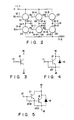
- Fig. 1A is a plan view of a semiconductor structure obtained in an assembling step of a 3-phase bridge converting circuit module according to one embodiment of this invention
- Fig. 1B is a side view of the 3-phase bridge converting circuit module shown in Fig. 1A.
- Lead frame 11 is formed of, for example, copper by punching a metal sheet with a thickness of 0.8 mm. Portion of lead frame 11 which is hatched in Fig. 1A is removed at the time of completion of the module.
- Switching circuits are formed on semiconductor chips Q1 to Q6.
- Outer lead 11-1 of lead frame 11 has mounting portion 11-1A for the semiconductor chips.
- Semiconductor chips Q1 to Q3 are mounted on mounting portion 11-1A by solder of Pb-Sb or the like.
- the first electrode (one terminal) of each of semiconductor chips Q1 to Q3 is connected to outer lead 11-1.
- Outer lead BU of lead frame 11 and the second electrode (control input terminal) of semiconductor chip Q1 are connected together by bonding wire 12-1 of A1 or the like.
- the wire bonding is attained by, for example, pressure bonding (US bonding).
- Outer lead U of lead frame 11 and the third electrode (the other terminal) of semiconductor chip Q1 are connected together by bonding wire 12-2.
- Outer lead BV of lead frame 11 and the second electrode of semiconductor chip Q2 are connected together by bonding wire 12-3.
- Outer lead V of lead frame 11 and the third electrode of semiconductor chip Q1 are connected together by bonding wire 12-4.
- Outer lead BW of lead frame 11 and the second electrode of semiconductor chip Q3 are connected together by bonding wire 12-5.
- Outer lead W of lead frame 11 and the third electrode of semiconductor chip Q3 are connected together by bonding wire 12-6.
- Semiconductor chip Q4 is mounted on lead 13-1 which is not externally derived.
- Lead 13-1 and the third electrode of semiconductor chip Q1 are connected together by bonding wire 12-7. Therefore, the first electrode of semiconductor chip Q4 is connected to outer lead U via lead 13-1, bonding wire 12-7, and bonding wire 12-2.
- Outer lead BX and the second electrode of semiconductor chip Q4 are connected together by bonding wire 12-8.
- Outer lead 11-2 and the third electrode of semiconductor chip Q4 are connected together by bonding wire 12-9.
- Semiconductor chip Q5 is mounted on lead 13-2 which is not externally derived. Lead 13-2 and the third electrode of semiconductor chip Q2 are connected together by bonding wire 12-10. Therefore, the first electrode of semiconductor chip Q5 is connected to outer lead V via lead 13-2, bonding wire 12-10, and bonding wire 12-4. Outer lead BY and the second electrode of semiconductor chip Q5 are connected together by bonding wire 12-11. Outer lead 11-2 and the third electrode of semiconductor chip Q5 are connected together by bonding wire 12-12. Semiconductor chip Q6 is mounted on lead 13-3 which is not externally derived. Lead 13-3 and the third electrode of semiconductor chip Q3 are connected together by bonding wire 12-13.
- the first electrode of semiconductor chip Q6 is connected to outer lead W via lead 13-3, bonding wire 12-13, and bonding wire 12-6.
- Outer lead BZ and the second electrode of semiconductor chip Q6 are connected together by bonding wire 12-14.
- Outer lead 11-2 and the third electrode of semiconductor chip Q6 are connected together by bonding wire 12-15.
- SIP type package 14 (shown by broken lines).
- outer lead 12-3 is cut off inside package 14 and is not used for the circuit operation.
- Fig. 2 is a circuit diagram of the module shown in Figs. 1A and 1B and formed to function as a 3-phase bridge inverting circuit.
- a positive DC power source + is connected to outer lead 11-1 and the ground terminal is connected to outer lead 11-2.
- Outer leads U, V and W are used as 3-phase output terminals.
- Outer leads BU, BV, BW, BX, BY and BZ are used as control input terminals.
- 3-phase signals are output from outer leads U, V and W according to control signals from outer leads BU, BV, BW, BX, BY and BZ.
- Figs. 3 to 5 shown the construction of switching circuits formed in semiconductor chips Q1 to Q6 shown in Fig. 2.
- Fig. 3 shows the switching circuit formed of NPN type bipolar transistor 15.
- collector terminals (corresponding to the first electrode described above) 16 of transistors 15 are commonly connected to outer lead 11-1
- base terminals (corresponding to the second electrode described above) 17 are respectively connected to outer leads BU, BV and BW
- emitter terminals (corresponding to the third electrode described above) 18 are respectively connected to outer leads U, V and W.
- collector terminals 16 of transistor 15 are respectively connected to outer leads U, V and W, base terminals 17 are respectively connected to outer leads BX, BY and BZ, and emitter terminals 18 are commonly connected to outer lead 11-2.
- Fig. 4 shows another construction of the switching circuit described above.
- protection diode 19 is connected to NPN type bipolar transistor 15 shown in Fig. 3.
- the anode of diode 19 is connected to the emitter of transistor 15 and the cathode is connected to the collector.
- the switching circuit of Fig. 4 is preferably used in the case where the inductance load is driven by 3-phase signals generated from outer leads U, V and W.
- a counter electromotive force is generated at the time of interruption of current supply.
- diode 19 permits the counter electromotive force to be transmitted from the positive terminal + to the ground therethrough, thus protecting transistor 15.
- Resistor 20 connected between the base and emitter of transistor 15 can be obtained as a parasitic resistance at the time of manufacturing the semiconductor chip.
- terminals 16, 17 and 18 are connected in the same manner as described with reference to the circuit of Fig. 3.
- NPN type bipolar transistor 21 is additionally connected to NPN type bipolar transistor 15 in the circuit of Fig. 4 in a Darlington fashion.
- Resistor 20A connected between the base and emitter of transistor 15, and resistor 20B connected between the base and emitter of transistor 21 can be obtained as a parasitic resistance at the time of manufacturing the semiconductor chip.
- the control signal amplified by Darlington connected transistors 21 and 15 so that a sufficiently large driving ability can be attained.
- terminals 16, 17 and 18 are connected in the same manner as described with reference to the circuits of Figs. 3 and 4.
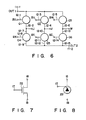
- Fig. 6 shows the construction of a circuit obtained in the case where the module shown in Figs. 1A and 1B is used as a 3-phase bridge converting circuit for AC-DC conversion.
- outer leads 11-1 and 11-2 are used as DC output terminals OUT1 and OUT2.
- Outer leads U, V and W are used as input terminals for 3-phase signals.
- Outer leads BU, BV, BW, BX, BY and BZ are used as control input terminals.
- Figs. 7 and 8 show the construction of switching circuits formed in semiconductor chips of Fig. 6.
- Fig. 7 shows the switching circuit formed of MOSFET 22.
- source terminals 16 of the MOSFET are commonly connected to outer lead 11-1
- gate terminals 17 are respectively connected to outer leads BU, BV and BW
- drain terminals 18 are respectively connected to outer leads U, V and W.
- drain terminals 18 of MOSFET 22 are respectively connected to outer leads U, V and W
- gate terminals 17 are respectively connected to outer leads BX, BY and BZ
- source terminals 16 are commonly connected to outer lead 11-2.
- Fig. 8 shows the switching circuits formed to function as thyristor 23.
- semiconductor chips Q1 to Q3 cathode terminals 16 of thyristor 23 are commonly connected to outer lead 11-1
- gate terminals 17 are respectively connected to outer leads BU, BV and BW
- anode terminals 18 are respectively connected to outer leads U, V and W.
- cathode terminals 16 of thyristor 23 are respectively connected to outer leads U, V and W
- gate terminals 17 are respectively connected to outer leads BX, BY and BZ
- anode terminals 18 are commonly connected to outer lead 11-2.
- a complicated wiring of the 3-phase bridge converting circuit module is arranged on the bridge wiring side or in the module.
- outer leads U, V and W are arranged in the order of generation of output signals, the circuit pattern on the PC board can be simplified. It is not necessary to additionally provide a wiring using jumper lines or the like and the mounting step can be simplified. Further, the circuit pattern can be made wide due to the simplification of the circuit pattern on the PC board, and therefore the 3-phase bridge converting circuit module can be used for large power elements.
- outer leads BU, U, BV, V, BW and W it is not always necessary to arrange outer leads BU, U, BV, V, BW and W in the order described above, and it is only necessary to arrange to make pairs of outer leads BU and U; BV and V; and BW and W. Further, it is not necessary to arrange outer leads BX, BY, BZ and 11-2 in the order described above, but it is necessary to arrange outer leads BX, BY, BW and 11-2 together in one place. Since voltage applied to outer leads BX, BY, BZ and 11-2 is low, the outer leads can be arranged with a small distance from one another in order to reduce the size of the SIP package.
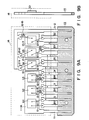
- Figs. 9A and 9B are plan and side views of a semiconductor structure obtained in an assembling step of a 3-phase bridge converting circuit module according to another embodiment of this invention.
- those portions which correspond to portions of Figs. 1A and 1B are denoted by the same numerals.
- the semiconductor structure of Figs. 9A and 9B is simpler to that of Figs. 1A and 1B except the form of the pattern of lead frame 11 and the wiring pattern.
- the arrangement of outer leads 11-1, BU, U, BV, V, BW, W, BX, BY and BZ is the same as in Figs. 1A and 1B.
- lead 13-1 and outer lead U are connected together by means of bonding wire 24-1 instead of using lead 13-1 and bonding wire 12-7, 12-2 to connect one terminal of semiconductor chip Q4 and outer lead U together.
- Lead 13-2 and outer lead V are connected together by means of bonding wire 24-2 instead of using lead 13-2 and bonding wire 12-10, 12-4 to connect one terminal of semiconductor chip Q5 and outer lead V together.
- lead 13-3 and outer lead W are connected together by means of bonding wire 24-3 instead of using lead 13-3 and bonding wire 12-13, 12-6 to connect one terminal of semiconductor chip Q6 and outer lead W together. Connections between leads 13-1 to 13-3 and outer leads U, V and W are effected inside package 14.
- the circuit pattern on the PC board can be simplified. Since it is not necessary to additionally provide a wiring using jumper lines or the like, the mounting step can be simplified. Further, the circuit pattern can be made wide due to the simplification of the circuit pattern on the PC board, and therefore the 3-phase bridge converting circuit module can be used for large power elements.
- connection is made by means of bonding wires 24-1 to 24-3.
- bonding wires 24-1 to 24-3 it is possible to weld a jumper wiring board to attain the same connection.
Landscapes
- Engineering & Computer Science (AREA)
- Power Engineering (AREA)
- Microelectronics & Electronic Packaging (AREA)
- Computer Hardware Design (AREA)
- Physics & Mathematics (AREA)
- Condensed Matter Physics & Semiconductors (AREA)
- General Physics & Mathematics (AREA)
- Inverter Devices (AREA)
Applications Claiming Priority (2)
| Application Number | Priority Date | Filing Date | Title |
|---|---|---|---|
| JP37781/87 | 1987-02-23 | ||
| JP62037781A JPH0740790B2 (ja) | 1987-02-23 | 1987-02-23 | 大電力パワ−モジユ−ル |
Publications (2)
| Publication Number | Publication Date |
|---|---|
| EP0280235A2 true EP0280235A2 (de) | 1988-08-31 |
| EP0280235A3 EP0280235A3 (de) | 1989-03-15 |
Family
ID=12507030
Family Applications (1)
| Application Number | Title | Priority Date | Filing Date |
|---|---|---|---|
| EP19880102573 Withdrawn EP0280235A3 (de) | 1987-02-23 | 1988-02-22 | Dreiphasiger Umformermodul mit Brückenschaltung |
Country Status (5)
| Country | Link |
|---|---|
| US (1) | US4862344A (de) |
| EP (1) | EP0280235A3 (de) |
| JP (1) | JPH0740790B2 (de) |
| KR (1) | KR960000799B1 (de) |
| CN (1) | CN1005673B (de) |
Cited By (5)
| Publication number | Priority date | Publication date | Assignee | Title |
|---|---|---|---|---|
| EP0443044A1 (de) * | 1989-09-12 | 1991-08-28 | Kabushiki Kaisha Toshiba | Leitergitter für halbleiteranordnung und halbleiteranordnung mit diesem leitergitter |
| EP0578991A1 (de) * | 1992-07-13 | 1994-01-19 | Asea Brown Boveri Ag | Bidirektionaler Halbleiterschalter |
| WO1996008842A1 (en) * | 1994-09-15 | 1996-03-21 | National Semiconductor Corporation | Electronic system circuit package |
| EP0696818A3 (de) * | 1994-08-12 | 1997-07-02 | Siemens Ag | Halbleiterbauelement mit isolierendem Gehäuse |
| EP1818983A2 (de) * | 2006-01-17 | 2007-08-15 | International Rectifier Corporation | Dreiphasen-Wechselrichterleistungsstufe und Montage |
Families Citing this family (14)
| Publication number | Priority date | Publication date | Assignee | Title |
|---|---|---|---|---|
| US5043859A (en) * | 1989-12-21 | 1991-08-27 | General Electric Company | Half bridge device package, packaged devices and circuits |
| JPH0834709B2 (ja) * | 1990-01-31 | 1996-03-29 | 株式会社日立製作所 | 半導体集積回路及びそれを使つた電動機制御装置 |
| US5184291A (en) * | 1991-06-13 | 1993-02-02 | Crowe Lawrence E | Converter and inverter support module |
| US5170337A (en) * | 1992-01-29 | 1992-12-08 | General Electric Company | Low-inductance package for multiple paralleled devices operating at high frequency |
| FR2687513B1 (fr) * | 1992-02-18 | 1995-11-24 | Int Rectifier Corp | Alimentation resonnante a auto-generation et procede de production d'energie pour un circuit de commutation a transistors. |
| JP3352840B2 (ja) * | 1994-03-14 | 2002-12-03 | 株式会社東芝 | 逆並列接続型双方向性半導体スイッチ |
| JPH0855956A (ja) * | 1994-08-10 | 1996-02-27 | Fuji Electric Co Ltd | 駆動回路装置モジュール |
| US6452254B2 (en) * | 2000-05-01 | 2002-09-17 | Agere Systems Guardian Corp. | Optical package with dual interconnect capability |
| US8120161B2 (en) * | 2007-04-10 | 2012-02-21 | Infineon Technologies Ag | Semiconductor module including semiconductor chips coupled to external contact elements |
| DE102007016901B4 (de) * | 2007-04-10 | 2012-01-26 | Infineon Technologies Ag | Halbleiterbauelement und elektronisches Modul |
| US8227908B2 (en) * | 2008-07-07 | 2012-07-24 | Infineon Technologies Ag | Electronic device having contact elements with a specified cross section and manufacturing thereof |
| JP5407674B2 (ja) * | 2009-09-02 | 2014-02-05 | サンケン電気株式会社 | 半導体装置 |
| JP5097797B2 (ja) * | 2010-05-31 | 2012-12-12 | 日立オートモティブシステムズ株式会社 | 電力変換装置及びそれを備えた移動体 |
| CN107112317B (zh) * | 2014-12-24 | 2019-07-05 | 日本精工株式会社 | 功率半导体模块以及使用其的电动助力转向装置 |
Citations (5)
| Publication number | Priority date | Publication date | Assignee | Title |
|---|---|---|---|---|
| DE2940148A1 (de) * | 1978-10-05 | 1980-04-24 | Aizu Toko K K | Variable kapazitaetsdiodenanordnung |
| EP0058852A2 (de) * | 1981-02-20 | 1982-09-01 | Siemens Aktiengesellschaft | Halbleiteranordnung mit aus Blech ausgeschnittenen Anschlussleitern |
| EP0064856A2 (de) * | 1981-05-12 | 1982-11-17 | LUCAS INDUSTRIES public limited company | Multiphasen-Brückenanordnung |
| DE3336979A1 (de) * | 1982-10-12 | 1984-04-26 | Mitsubishi Denki K.K., Tokio/Tokyo | Abschalt-thyristor modul |
| DE3516995A1 (de) * | 1984-05-11 | 1985-11-14 | Mitsubishi Denki K.K., Tokio/Tokyo | Halbleitereinrichtung |
Family Cites Families (5)
| Publication number | Priority date | Publication date | Assignee | Title |
|---|---|---|---|---|
| US3081424A (en) * | 1960-01-11 | 1963-03-12 | Ite Circuit Breaker Ltd | Semi-conductor rectifier bridge construction |
| JPS5715442A (en) * | 1980-07-02 | 1982-01-26 | Fujitsu Ltd | Production of semiconductor device |
| JPS6157540U (de) * | 1984-09-19 | 1986-04-17 | ||
| JPH0758748B2 (ja) * | 1984-12-25 | 1995-06-21 | 株式会社東芝 | 半導体装置 |
| JPS622587A (ja) * | 1985-06-28 | 1987-01-08 | 電気化学工業株式会社 | ハイパワ−用混成集積回路 |
-
1987
- 1987-02-23 JP JP62037781A patent/JPH0740790B2/ja not_active Expired - Fee Related
-
1988
- 1988-02-22 US US07/158,714 patent/US4862344A/en not_active Expired - Lifetime
- 1988-02-22 EP EP19880102573 patent/EP0280235A3/de not_active Withdrawn
- 1988-02-23 CN CN88101051.0A patent/CN1005673B/zh not_active Expired
- 1988-02-23 KR KR1019880001875A patent/KR960000799B1/ko not_active IP Right Cessation
Patent Citations (5)
| Publication number | Priority date | Publication date | Assignee | Title |
|---|---|---|---|---|
| DE2940148A1 (de) * | 1978-10-05 | 1980-04-24 | Aizu Toko K K | Variable kapazitaetsdiodenanordnung |
| EP0058852A2 (de) * | 1981-02-20 | 1982-09-01 | Siemens Aktiengesellschaft | Halbleiteranordnung mit aus Blech ausgeschnittenen Anschlussleitern |
| EP0064856A2 (de) * | 1981-05-12 | 1982-11-17 | LUCAS INDUSTRIES public limited company | Multiphasen-Brückenanordnung |
| DE3336979A1 (de) * | 1982-10-12 | 1984-04-26 | Mitsubishi Denki K.K., Tokio/Tokyo | Abschalt-thyristor modul |
| DE3516995A1 (de) * | 1984-05-11 | 1985-11-14 | Mitsubishi Denki K.K., Tokio/Tokyo | Halbleitereinrichtung |
Non-Patent Citations (1)
| Title |
|---|
| PATENT ABSTRACTS OF JAPAN, vol. 6, no. 77 (E-106)[955], 14th May 1982; & JP-A-57 015 452 (MITSUBISHI DENKI K.K.) 26-01-1982 * |
Cited By (7)
| Publication number | Priority date | Publication date | Assignee | Title |
|---|---|---|---|---|
| EP0443044A1 (de) * | 1989-09-12 | 1991-08-28 | Kabushiki Kaisha Toshiba | Leitergitter für halbleiteranordnung und halbleiteranordnung mit diesem leitergitter |
| EP0443044A4 (en) * | 1989-09-12 | 1993-04-14 | Kabushiki Kaisha Toshiba | Lead frame for semiconductor device and semiconductor device using the lead frame |
| EP0578991A1 (de) * | 1992-07-13 | 1994-01-19 | Asea Brown Boveri Ag | Bidirektionaler Halbleiterschalter |
| EP0696818A3 (de) * | 1994-08-12 | 1997-07-02 | Siemens Ag | Halbleiterbauelement mit isolierendem Gehäuse |
| WO1996008842A1 (en) * | 1994-09-15 | 1996-03-21 | National Semiconductor Corporation | Electronic system circuit package |
| EP1818983A2 (de) * | 2006-01-17 | 2007-08-15 | International Rectifier Corporation | Dreiphasen-Wechselrichterleistungsstufe und Montage |
| EP1818983A3 (de) * | 2006-01-17 | 2009-07-29 | Siliconix Technology C.V. | Dreiphasen-Wechselrichterleistungsstufe und Montage |
Also Published As
| Publication number | Publication date |
|---|---|
| JPH0740790B2 (ja) | 1995-05-01 |
| KR880010549A (ko) | 1988-10-10 |
| US4862344A (en) | 1989-08-29 |
| KR960000799B1 (ko) | 1996-01-12 |
| CN1005673B (zh) | 1989-11-01 |
| CN88101051A (zh) | 1988-09-21 |
| EP0280235A3 (de) | 1989-03-15 |
| JPS63206166A (ja) | 1988-08-25 |
Similar Documents
| Publication | Publication Date | Title |
|---|---|---|
| US4862344A (en) | 3-phase bridge converting circuit module | |
| US5942797A (en) | Power semiconductor module | |
| US8115294B2 (en) | Multichip module with improved system carrier | |
| US6166464A (en) | Power module | |
| US7880288B2 (en) | Semiconductor module with semiconductor chips and method for producing it | |
| US7095099B2 (en) | Low profile package having multiple die | |
| US7592688B2 (en) | Semiconductor package | |
| JP6455364B2 (ja) | 半導体装置、インテリジェントパワーモジュールおよび電力変換装置 | |
| US20030107120A1 (en) | Intelligent motor drive module with injection molded package | |
| US9468087B1 (en) | Power module with improved cooling and method for making | |
| JP2002110905A (ja) | 半導体装置 | |
| EP0697732A2 (de) | Steuerschaltungsmodul | |
| US5541453A (en) | Power semiconductor module | |
| US7177128B2 (en) | Snubber module and power conversion device | |
| JP2008218688A (ja) | 半導体装置 | |
| US10083935B2 (en) | Semiconductor device and a manufacturing method of the semiconductor device | |
| JP2006165322A (ja) | 半導体モジュール | |
| JP4246040B2 (ja) | 半導体装置の実装体 | |
| JP2006294973A (ja) | 半導体装置 | |
| JP2001102518A (ja) | 電力用半導体装置 | |
| US10855274B2 (en) | Semiconductor device | |
| CN220569660U (zh) | 一种基于覆铜陶瓷基板的igbt封装结构 | |
| US20230307430A1 (en) | Semiconductor device | |
| US20230230940A1 (en) | Semiconductor device | |
| KR100344225B1 (ko) | 전력 반도체 모듈의 수분침투 방지장치 |
Legal Events
| Date | Code | Title | Description |
|---|---|---|---|
| PUAI | Public reference made under article 153(3) epc to a published international application that has entered the european phase |
Free format text: ORIGINAL CODE: 0009012 |
|
| 17P | Request for examination filed |
Effective date: 19880318 |
|
| AK | Designated contracting states |
Kind code of ref document: A2 Designated state(s): DE FR GB IT |
|
| PUAL | Search report despatched |
Free format text: ORIGINAL CODE: 0009013 |
|
| AK | Designated contracting states |
Kind code of ref document: A3 Designated state(s): DE FR GB IT |
|
| 17Q | First examination report despatched |
Effective date: 19910422 |
|
| STAA | Information on the status of an ep patent application or granted ep patent |
Free format text: STATUS: THE APPLICATION IS DEEMED TO BE WITHDRAWN |
|
| 18D | Application deemed to be withdrawn |
Effective date: 19930330 |