EP0277828A2 - Composé formant un film mince pour masque - Google Patents
Composé formant un film mince pour masque Download PDFInfo
- Publication number
- EP0277828A2 EP0277828A2 EP88300920A EP88300920A EP0277828A2 EP 0277828 A2 EP0277828 A2 EP 0277828A2 EP 88300920 A EP88300920 A EP 88300920A EP 88300920 A EP88300920 A EP 88300920A EP 0277828 A2 EP0277828 A2 EP 0277828A2
- Authority
- EP
- European Patent Office
- Prior art keywords
- coating layer
- light
- copper
- layer
- graphic artwork
- Prior art date
- Legal status (The legal status is an assumption and is not a legal conclusion. Google has not performed a legal analysis and makes no representation as to the accuracy of the status listed.)
- Granted
Links
- 239000010409 thin film Substances 0.000 title claims abstract description 8
- 150000001875 compounds Chemical class 0.000 title description 3
- 239000011247 coating layer Substances 0.000 claims abstract description 69
- NLXLAEXVIDQMFP-UHFFFAOYSA-N Ammonia chloride Chemical compound [NH4+].[Cl-] NLXLAEXVIDQMFP-UHFFFAOYSA-N 0.000 claims abstract description 26
- RYGMFSIKBFXOCR-UHFFFAOYSA-N Copper Chemical compound [Cu] RYGMFSIKBFXOCR-UHFFFAOYSA-N 0.000 claims abstract description 25
- 229910052802 copper Inorganic materials 0.000 claims abstract description 21
- 239000010949 copper Substances 0.000 claims abstract description 21
- QPLDLSVMHZLSFG-UHFFFAOYSA-N Copper oxide Chemical compound [Cu]=O QPLDLSVMHZLSFG-UHFFFAOYSA-N 0.000 claims abstract description 18
- 239000005751 Copper oxide Substances 0.000 claims abstract description 17
- 229910000431 copper oxide Inorganic materials 0.000 claims abstract description 17
- MHAJPDPJQMAIIY-UHFFFAOYSA-N Hydrogen peroxide Chemical compound OO MHAJPDPJQMAIIY-UHFFFAOYSA-N 0.000 claims abstract description 15
- 235000019270 ammonium chloride Nutrition 0.000 claims abstract description 13
- 238000005530 etching Methods 0.000 claims abstract description 10
- 239000000203 mixture Substances 0.000 claims abstract description 10
- 239000000758 substrate Substances 0.000 claims description 25
- 239000010410 layer Substances 0.000 claims description 19
- 238000004544 sputter deposition Methods 0.000 claims description 18
- 238000000034 method Methods 0.000 claims description 16
- 230000005855 radiation Effects 0.000 claims description 14
- 229910052751 metal Inorganic materials 0.000 claims description 13
- 239000002184 metal Substances 0.000 claims description 13
- 230000036961 partial effect Effects 0.000 claims description 12
- 239000000463 material Substances 0.000 claims description 9
- 230000003287 optical effect Effects 0.000 claims description 9
- QVGXLLKOCUKJST-UHFFFAOYSA-N atomic oxygen Chemical compound [O] QVGXLLKOCUKJST-UHFFFAOYSA-N 0.000 claims description 7
- 239000002923 metal particle Substances 0.000 claims description 7
- 239000001301 oxygen Substances 0.000 claims description 7
- 229910052760 oxygen Inorganic materials 0.000 claims description 7
- 230000005540 biological transmission Effects 0.000 claims description 6
- BERDEBHAJNAUOM-UHFFFAOYSA-N copper(I) oxide Inorganic materials [Cu]O[Cu] BERDEBHAJNAUOM-UHFFFAOYSA-N 0.000 claims description 6
- KRFJLUBVMFXRPN-UHFFFAOYSA-N cuprous oxide Chemical compound [O-2].[Cu+].[Cu+] KRFJLUBVMFXRPN-UHFFFAOYSA-N 0.000 claims description 6
- 239000010408 film Substances 0.000 claims description 2
- 238000004519 manufacturing process Methods 0.000 claims description 2
- 230000000903 blocking effect Effects 0.000 claims 7
- 238000002834 transmittance Methods 0.000 claims 6
- 238000009501 film coating Methods 0.000 abstract description 2
- 239000011248 coating agent Substances 0.000 description 15
- 238000000576 coating method Methods 0.000 description 15
- XKRFYHLGVUSROY-UHFFFAOYSA-N Argon Chemical compound [Ar] XKRFYHLGVUSROY-UHFFFAOYSA-N 0.000 description 6
- 239000007789 gas Substances 0.000 description 6
- 150000002739 metals Chemical class 0.000 description 4
- 230000000007 visual effect Effects 0.000 description 4
- 229910052786 argon Inorganic materials 0.000 description 3
- 239000003518 caustics Substances 0.000 description 3
- 229910016553 CuOx Inorganic materials 0.000 description 2
- MYMOFIZGZYHOMD-UHFFFAOYSA-N Dioxygen Chemical compound O=O MYMOFIZGZYHOMD-UHFFFAOYSA-N 0.000 description 2
- HCHKCACWOHOZIP-UHFFFAOYSA-N Zinc Chemical compound [Zn] HCHKCACWOHOZIP-UHFFFAOYSA-N 0.000 description 2
- 239000011195 cermet Substances 0.000 description 2
- 238000000151 deposition Methods 0.000 description 2
- 229910001882 dioxygen Inorganic materials 0.000 description 2
- 238000001755 magnetron sputter deposition Methods 0.000 description 2
- 230000000873 masking effect Effects 0.000 description 2
- 229920006267 polyester film Polymers 0.000 description 2
- 238000005546 reactive sputtering Methods 0.000 description 2
- 238000000411 transmission spectrum Methods 0.000 description 2
- XLYOFNOQVPJJNP-UHFFFAOYSA-N water Substances O XLYOFNOQVPJJNP-UHFFFAOYSA-N 0.000 description 2
- 229910052725 zinc Inorganic materials 0.000 description 2
- 239000011701 zinc Substances 0.000 description 2
- 229910052782 aluminium Inorganic materials 0.000 description 1
- XAGFODPZIPBFFR-UHFFFAOYSA-N aluminium Chemical compound [Al] XAGFODPZIPBFFR-UHFFFAOYSA-N 0.000 description 1
- 238000012512 characterization method Methods 0.000 description 1
- BGTFCAQCKWKTRL-YDEUACAXSA-N chembl1095986 Chemical compound C1[C@@H](N)[C@@H](O)[C@H](C)O[C@H]1O[C@@H]([C@H]1C(N[C@H](C2=CC(O)=CC(O[C@@H]3[C@H]([C@@H](O)[C@H](O)[C@@H](CO)O3)O)=C2C=2C(O)=CC=C(C=2)[C@@H](NC(=O)[C@@H]2NC(=O)[C@@H]3C=4C=C(C(=C(O)C=4)C)OC=4C(O)=CC=C(C=4)[C@@H](N)C(=O)N[C@@H](C(=O)N3)[C@H](O)C=3C=CC(O4)=CC=3)C(=O)N1)C(O)=O)=O)C(C=C1)=CC=C1OC1=C(O[C@@H]3[C@H]([C@H](O)[C@@H](O)[C@H](CO[C@@H]5[C@H]([C@@H](O)[C@H](O)[C@@H](C)O5)O)O3)O[C@@H]3[C@H]([C@@H](O)[C@H](O)[C@@H](CO)O3)O[C@@H]3[C@H]([C@H](O)[C@@H](CO)O3)O)C4=CC2=C1 BGTFCAQCKWKTRL-YDEUACAXSA-N 0.000 description 1
- 239000003086 colorant Substances 0.000 description 1
- 238000007796 conventional method Methods 0.000 description 1
- 230000008021 deposition Effects 0.000 description 1
- 230000005684 electric field Effects 0.000 description 1
- 229910052732 germanium Inorganic materials 0.000 description 1
- GNPVGFCGXDBREM-UHFFFAOYSA-N germanium atom Chemical compound [Ge] GNPVGFCGXDBREM-UHFFFAOYSA-N 0.000 description 1
- 239000011261 inert gas Substances 0.000 description 1
- 238000009413 insulation Methods 0.000 description 1
- 239000007788 liquid Substances 0.000 description 1
- 230000001590 oxidative effect Effects 0.000 description 1
- 229920002120 photoresistant polymer Polymers 0.000 description 1
- 239000002985 plastic film Substances 0.000 description 1
- 229920006255 plastic film Polymers 0.000 description 1
- 229920000728 polyester Polymers 0.000 description 1
- 210000004994 reproductive system Anatomy 0.000 description 1
- 238000007789 sealing Methods 0.000 description 1
- 238000000926 separation method Methods 0.000 description 1
- 229910001220 stainless steel Inorganic materials 0.000 description 1
- 239000010935 stainless steel Substances 0.000 description 1
Images

Classifications
-
- H—ELECTRICITY
- H05—ELECTRIC TECHNIQUES NOT OTHERWISE PROVIDED FOR
- H05K—PRINTED CIRCUITS; CASINGS OR CONSTRUCTIONAL DETAILS OF ELECTRIC APPARATUS; MANUFACTURE OF ASSEMBLAGES OF ELECTRICAL COMPONENTS
- H05K3/00—Apparatus or processes for manufacturing printed circuits
-
- G—PHYSICS
- G03—PHOTOGRAPHY; CINEMATOGRAPHY; ANALOGOUS TECHNIQUES USING WAVES OTHER THAN OPTICAL WAVES; ELECTROGRAPHY; HOLOGRAPHY
- G03F—PHOTOMECHANICAL PRODUCTION OF TEXTURED OR PATTERNED SURFACES, e.g. FOR PRINTING, FOR PROCESSING OF SEMICONDUCTOR DEVICES; MATERIALS THEREFOR; ORIGINALS THEREFOR; APPARATUS SPECIALLY ADAPTED THEREFOR
- G03F1/00—Originals for photomechanical production of textured or patterned surfaces, e.g., masks, photo-masks, reticles; Mask blanks or pellicles therefor; Containers specially adapted therefor; Preparation thereof
- G03F1/54—Absorbers, e.g. of opaque materials
-
- G—PHYSICS
- G03—PHOTOGRAPHY; CINEMATOGRAPHY; ANALOGOUS TECHNIQUES USING WAVES OTHER THAN OPTICAL WAVES; ELECTROGRAPHY; HOLOGRAPHY
- G03F—PHOTOMECHANICAL PRODUCTION OF TEXTURED OR PATTERNED SURFACES, e.g. FOR PRINTING, FOR PROCESSING OF SEMICONDUCTOR DEVICES; MATERIALS THEREFOR; ORIGINALS THEREFOR; APPARATUS SPECIALLY ADAPTED THEREFOR
- G03F1/00—Originals for photomechanical production of textured or patterned surfaces, e.g., masks, photo-masks, reticles; Mask blanks or pellicles therefor; Containers specially adapted therefor; Preparation thereof
- G03F1/68—Preparation processes not covered by groups G03F1/20 - G03F1/50
- G03F1/80—Etching
-
- H—ELECTRICITY
- H05—ELECTRIC TECHNIQUES NOT OTHERWISE PROVIDED FOR
- H05K—PRINTED CIRCUITS; CASINGS OR CONSTRUCTIONAL DETAILS OF ELECTRIC APPARATUS; MANUFACTURE OF ASSEMBLAGES OF ELECTRICAL COMPONENTS
- H05K3/00—Apparatus or processes for manufacturing printed circuits
- H05K3/0002—Apparatus or processes for manufacturing printed circuits for manufacturing artworks for printed circuits
Definitions
- the present invention relates to thin film compounds or coating layers which are opaque to ultraviolet light radiation, methods of etching such coating layers or compounds to produce masking patterns, resultant graphic artworks created thereby, and patterned products produced using such graphic artworks.
- thin film coatings for producing graphic artworks such as masks for printed circuits or photo tools for graphic printing have suffered from a variety of known disadvantages.
- germanium is a well known pound which is opaque to ultraviolet light and hence useful for producing patterned graphic artworks, but has an inherent disadvantage due to its high cost.
- Metals such as zinc or aluminum could be used for the production of graphic artworks since they are also opaque to ultraviolet light, but an accompanying disadvantage is that rather strong caustic solutions are required to appropriately etch these metals.
- Zinc has an additional disadvantage in that it is soft.
- metals are not transparent at visible light wavelengths and hence it is difficult to align a mask or graphic artwork using metals if the product being masked requires several superimposed pattern layers.
- a substrate including a coating layer which includes copper oxide, the coating layer consisting essentially of the copper oxide Cu2O according to one embodiment, and consisting essentially of a copper oxide plus unoxidized copper atoms according to another embodiment, the coating layer being deposited on a substrate as a thin film having a thickness less than 3000 angstroms for example, a patterned resist material being disposed over the coating layer so as to form a predetermined pattern on the coating layer, exposed portions of the coating layer thereafter being etched.
- the coating layer is etched using ammonium chloride when the coating layer consists essentially of copper oxide, and for the embodiment where the coating layer consists essentially of a copper oxide plus unoxidized copper atoms, ammonium chloride mixed with hydrogen peroxide is used for etching, the hydrogen peroxide oxidizing any non-oxidized copper atoms or molecules.
- the coating layer is deposited by planar magnetron reactive sputtering whereby a target being sputtered comprising essentially pure copper metal, with oxygen being introduced into the sputtering chamber as a gas.
- Optimum optical properties of the coating layer are determined by varying a sputtering power and an oxygen partial pressure within the sputtering chamber while measuring the resultant optical properties of the coating layers so produced using feedback control.
- the coating layer can be tailored so as to have a transmission to light having a wavelength between 300 and 400 nanometers which is less than 10%, preferably less than 1%, more preferably less than 0.1%, and optimally less than 0.01%.
- the coating layer can be tailored so as to have a transmission to visible light, e.g. light having a wavelength between 600 and 700 nanometers, which is greater than 20%, preferably greater than 40%, optimally greater than 60%.
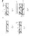
- Figure 1 illustrates a substrate 1 on which has been formed a coating layer 2
- Figure 2 illustrates the article of Figure 1 subsequent to a resist material 3 being formed on top of the coating layer 2 in a predetermined pattern.
- the substrate 1, the coating layer 2, and the pattern resist material 3 are exposed to an etching solution which selectively etches exposed portions 4 of the coating 2 rather than the resist material 3 so as to form the predetermined pattern on the substrate 1 and also on the coating layer 2, as illustrated in Figure 3.
- the graphic artwork 15 so produced is then used to transfer the predetermined pattern onto an appropriate medium, such as a printed circuit board 9 illustrated in Figure 4 so as to print circuit paths and circuit features corresponding to the predetermined pattern onto conducting layer 12 of the board 9.
- the printing is accomplished by disposing the graphic artwork or mask 15 over the printed circuit board 9 and exposing both the graphic artwork 15 and the printed circuit board 9 to ultraviolet light radiation 8.
- the radiation is transmitted through the graphic artwork 15 at all areas thereof where the coating layer 2 has previously been etched away thereby exposing an upper ultraviolet sensitive layer 13 of the printed circuit board along these areas, the ultraviolet light radiation being blocked by the graphic artwork at all locations where the coating layer 2 has not been previously removed.
- exposed portions of the ultraviolet sensitive layer 13 of the printed circuit board 9 are removed by conventional techniques, and portions of the metal layer 12 so exposed are then etched away so as to form the predetermined pattern within the metal layer 12 of the printed circuit board.
- a printed circuit board In practice, it is not atypical for a printed circuit board to have a plurality of stacked metal layers thereon each individually patterned in a preselected way, the plurality of layers being interconnected by vias or vertical circuit lines. Accordingly, it can be appreciated that for producing such multilayer printed circuit boards it is advantageous that the graphic artworks or masks used for printing the circuits on the various board layers be at least partially transparent at visual light wavelengths so as to assist in aligning the masks with alignment markings on the board or other patterns of a set of masks.
- the graphic artworks of the invention can be used in additional applications as well.
- masks are used for producing color printing plates. Since a plurality of such masks and associated plates need to be used to superimpose a plurality of colors for a single image to achieve good color resolution, it is particularly advantageous that the masks used to create these plates be semitransparent at visual wavelengths so as to allow the masks associated with any one image to be stacked to insure a partial image of each mask appropriately registers with partial images of each of the other masks.
- the coating layer 2 of the graphic artwork 15 comprises a copper oxide thin film, optimally having a thickness of between 300 and 3000 angstroms, preferably between 500 and 2000 angstroms, e.g. between 600 and 1200 angstroms, the copper oxide essentially corresponding to Cu2O.
- the oxide Cu2O is known to be formed according to the first embodiment since a color of the coating is yellowish, it is conceivable that the other oxide of copper, CuO, may also exist in small amounts in the coating layer of the first embodiment.
- the coating layer 2 comprises a copper oxide plus unoxidized copper metal particles, the coating layer having a volume average composition Cu2O x where x is less than 2.0, preferably less than 1.0.
- the coating layer of the second embodiment of the invention e.g., as a suboxide or as a cermet, due to its extremely thin layer structure and an inevitable random nature in which it must be deposited.
- the characterization of the coating layer as only one of a suboxide and a cermet is actually of only academic concern, the important characteristic of the coating being that unoxidized copper does exist, and hence the volume average composition of the coating layer compri ses CuO x where x is less than 1.0, and preferably less than 0.5.
- Preferred materials for the substrate include polyester and other types of thin plastic films.
- resist materials include Riston® manufactured by DuPont and AZ1350 liquid photoresist manufactured by Shipley.
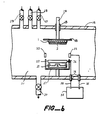
- a preferred method for forming the coating layer 2 on the substrate 1 is by planar magnetron reactive sputtering using an apparatus such as that illustrated in Figure 6.
- a target 2 which comprises a cathode, consists essentially of copper metal, and is located directly above a magnet 21 utilized for confining ionized gases in a region of the target 22, the gases to be ionized being injected into a sputtering chamber 31 via any one of inlet ports 27-29.
- An outlet port 30 is provided for evacuating the sputtering chamber 31.
- the copper is deposited onto the substrate 1 as the layer 2 by maintaining a voltage differential between the cathode copper target 22 and an anode 33 while introducing at least one inert gas such as argon into the sputtering chamber which is ionized by electric fields created within the sputtering chamber 1.
- the ionized gas causes metal particles to be knocked off the target 22 and to be sputter deposited onto the substrate 1.
- Figure l further shows a substrate holder 23, 24, a seal 25 for sealing between the holder portion 24 and a wall 26 of the sputtering chamber 31, a D.C. high voltage power source 35, insulation 36, a shielding box 37 disposed around the copper cathode target 22, and electrical connection cables 38 connected to the power source 35.
- An important embodiment of the invention is that oxygen is introduced into the sputtering chamber 31 via any one of the inlet ports 27-29 so that the copper metal particles are deposited onto the substrate as an oxide or suboxide, depending upon the partial pressure of oxygen within the sputtering chamber 31 and the sputtering power. Accordingly, if the substrate 1 is continuously transported across a sputtering region within the sputtering chamber 31 while a partial pressure of oxygen within the sputtering chamber 31 and/or a sputtering power is varied, it is possible to deposit various different coating layer positions onto the substrate 1 so as to obtain optimum optical properties. In addition, if the opaqueness or transparency of the coated substrate 1 is measured soon after sputtering at various light wavelengths, feedback control can also be incorporated so as to continuously vary various deposition parameters until an optimum coating layer composition is achieved.
- a pure copper oxide composition such as Cu2O
- a coating layer is essentially opaque to ultraviolet light having a wavelength from approximately 300 nanometers to 400 nanometers, and yet such a coating layer is also partially transparent at visible light wavelengths and in fact appears visually as yellowish.
- Such a coating layer is extremely advantageous where at least partial visual light transparency is required for a graphic artwork such as for example where registration at a particular location on a printed circuit board or other article to be produced is required.
- a coating layer further including unoxidized copper oxide is more desirous since the resultant coating layer is even more opaque to ultraviolet light radiation, though in general a copper oxide including nonoxidized copper is also more opaque at visual light wavelengths hence making registering difficult if necessary.
- the copper oxide and copper oxide including nonoxidized copper of the invention have several significant advantages over prior art coating layers used for masks and other types of graphic artworks.
- these coating layers are extremely environmentally stable, second they are easily produced and optimized using reactive magnetron sputtering tech niques, and third it is possible to etch such coating layers with materials that are non-caustic and relatively environmentally benign.
- the coating layers of the invention can be produced as extremely thin layers, as mentioned typically between 300 and 3000 angstroms thick, preferably between 500 and 1500 angstroms thick, optimally between 600 and 1200 angstroms thick, and are very fine grained, so that they can be etched to form extremely fine line patterns.
- optical properties of these coating layers can be readily adapted to meet optimum requirements for any particular photo reproductive system.
- the invention further includes a novel method for etching coating layers of the invention, these coating layers being etched by using a solution of ammonium chloride and hydrogen peroxide.
- ammonium chloride is sufficient to etch the coating layer completely.
- the coating layer also comprises unoxidized copper
- ammonium chloride is not capable of etching the unoxidized copper metal particles, and accordingly the use of hydrogen peroxide in conjunction with the ammonium chloride results in the copper being fully oxidizible and hence fully removable in the solution.
- An eighteen inch diameter stainless steel bell jar vacuum chamber was fitted with a planar magnetron sputtering source with an 8 ⁇ ⁇ 3 ⁇ target surface and a 12 ⁇ diameter rotating drum substrate holder around which a substrate of flexible film would be wrapped.
- the target to substrate separation was 21 ⁇ 2 ⁇ .
- the planar magnetron source was filled with a 99.9% pure copper target, and a substrate of 4 mil thick PET polyester film substrate was wrapped around the drum.
- the chamber was evacuated to a pressure of 1.8 ⁇ 10 ⁇ 5 Torr, then the following coating conditions were met: partial pressure of argon gas, 2.0 mTorr; partial pressure of oxygen gas, 0.30 mTorr; sputtering power, 500 watts; drum speed, 0.19 rpm; coating time, 25 sec.
- the resulting coating had a composition consisting essentially of Cu2O, a visible light transmission of 60%, a yellow color, and a transmission spectrum as shown in Figure 7. It was less than 1% transparent to ultraviolet radiation of wavelengths less than 400 mm.
- This coating could be completely removed by immersing it for 20 sec. in a solution of 27% (by weight) of ammonium chloride in water at 20 degrees for 20 seconds.
- the coating was however quite stable, and showed no change in properties after extended periods in air, at 80 degrees dry heat, and at 60 degrees C, 95% RH environments.
- Example 1 The apparatus used in Example 1 was used to coat a piece of 4 mil thick PET polyester film in the same manner as was used in Example 1, using the following conditions.
- the chamber was evacuated to a pressure of 1.8 ⁇ 10 ⁇ 5 Torr, then backfilled with argon gas to a partial pressure of 2.0 mTorr and oxygen gas to a partial pressure of 0.8 mTorr.
- the target was then sputtered in this atmosphere at a power of 1000 watts for twelve minutes, while the substrate drum was rotated at a speed of 0.5 rpm.
- the resulting coating had a composition CuO x where x was less than 0.5, had an optical density of 2.67 for visible light, and a transmission spectrum as shown in Figure 2. It was less than 0.1% transparent to ultraviolet radiation of wavelengths less than 400 mm.
- This coating could be completely removed by immersing it for 20 seconds in a solution of 27% ammonium chloride in water plus 7 ml of 3% hydrogen peroxide solution per 100 ml of ammonium chloride solution, at 20 degrees C.
- the coating was however quite stable, and showed no change in properties after extended periods in air, 80 degrees C dry heat and 60 degrees C 95% RH, environments.
Landscapes
- Physics & Mathematics (AREA)
- General Physics & Mathematics (AREA)
- Engineering & Computer Science (AREA)
- Manufacturing & Machinery (AREA)
- Microelectronics & Electronic Packaging (AREA)
- Manufacturing Of Printed Circuit Boards (AREA)
- Laminated Bodies (AREA)
- Physical Vapour Deposition (AREA)
- Materials For Photolithography (AREA)
- Photosensitive Polymer And Photoresist Processing (AREA)
- Surface Treatment Of Glass (AREA)
- Preparing Plates And Mask In Photomechanical Process (AREA)
Priority Applications (1)
| Application Number | Priority Date | Filing Date | Title |
|---|---|---|---|
| AT88300920T ATE75860T1 (de) | 1987-02-04 | 1988-02-03 | Duennschicht-zusammensetzungen fuer maske. |
Applications Claiming Priority (2)
| Application Number | Priority Date | Filing Date | Title |
|---|---|---|---|
| US10873 | 1987-02-04 | ||
| US07/010,873 US4911785A (en) | 1987-02-04 | 1987-02-04 | The method of forming a thin film artwork compounds |
Publications (3)
| Publication Number | Publication Date |
|---|---|
| EP0277828A2 true EP0277828A2 (fr) | 1988-08-10 |
| EP0277828A3 EP0277828A3 (en) | 1988-09-14 |
| EP0277828B1 EP0277828B1 (fr) | 1992-05-06 |
Family
ID=21747821
Family Applications (1)
| Application Number | Title | Priority Date | Filing Date |
|---|---|---|---|
| EP88300920A Expired - Lifetime EP0277828B1 (fr) | 1987-02-04 | 1988-02-03 | Composé formant un film mince pour masque |
Country Status (7)
| Country | Link |
|---|---|
| US (1) | US4911785A (fr) |
| EP (1) | EP0277828B1 (fr) |
| JP (1) | JPS63239453A (fr) |
| KR (1) | KR880010640A (fr) |
| AT (1) | ATE75860T1 (fr) |
| CA (1) | CA1308293C (fr) |
| DE (1) | DE3870638D1 (fr) |
Cited By (1)
| Publication number | Priority date | Publication date | Assignee | Title |
|---|---|---|---|---|
| WO1990008347A1 (fr) * | 1989-01-13 | 1990-07-26 | Andus Corporation | Traitement de surface pour revetements minces d'oxydes metalliques ou semi-conducteurs |
Families Citing this family (3)
| Publication number | Priority date | Publication date | Assignee | Title |
|---|---|---|---|---|
| US5011569A (en) * | 1987-02-04 | 1991-04-30 | Andus Corporation | Thin film artwork compounds |
| US6120693A (en) * | 1998-11-06 | 2000-09-19 | Alliedsignal Inc. | Method of manufacturing an interlayer via and a laminate precursor useful for same |
| US6707152B1 (en) * | 1999-04-16 | 2004-03-16 | Micron Technology, Inc. | Semiconductor device, electrical conductor system, and method of making |
Family Cites Families (26)
| Publication number | Priority date | Publication date | Assignee | Title |
|---|---|---|---|---|
| US2825687A (en) * | 1952-04-04 | 1958-03-04 | Nat Res Dev | Transparent conducting films |
| DE946588C (de) * | 1954-01-25 | 1956-08-02 | Wenczler & Heidenhain | Verfahren zum Aufbringen von Kopien auf beliebiges Material |
| US3705061A (en) * | 1971-03-19 | 1972-12-05 | Southern California Chem Co In | Continuous redox process for dissolving copper |
| US4123309A (en) * | 1973-11-29 | 1978-10-31 | Minnesota Mining And Manufacturing Company | Transfer letter system |
| US3822155A (en) * | 1973-01-22 | 1974-07-02 | Rca Corp | Method of making a semitransparent photomask |
| JPS50902A (fr) * | 1973-05-04 | 1975-01-08 | ||
| JPS5230848B2 (fr) * | 1973-10-09 | 1977-08-11 | ||
| US3919100A (en) * | 1974-04-24 | 1975-11-11 | Enthone | Alkaline etchant compositions |
| US4039698A (en) * | 1976-01-23 | 1977-08-02 | Bell Telephone Laboratories, Incorporated | Method for making patterned platinum metallization |
| US4319955A (en) * | 1980-11-05 | 1982-03-16 | Philip A. Hunt Chemical Corp. | Ammoniacal alkaline cupric etchant solution for and method of reducing etchant undercut |
| US4379040A (en) * | 1981-01-29 | 1983-04-05 | Ppg Industries, Inc. | Method of and apparatus for control of reactive sputtering deposition |
| US4336119A (en) * | 1981-01-29 | 1982-06-22 | Ppg Industries, Inc. | Method of and apparatus for control of reactive sputtering deposition |
| US4387156A (en) * | 1981-02-04 | 1983-06-07 | Minnesota Mining And Manufacturing Company | Imageable film containing a metal oxide opacifying layer |
| US4451327A (en) * | 1982-12-17 | 1984-05-29 | Psi Star, Inc. | Process and structure for etching copper |
| JPS59150453A (ja) * | 1982-12-23 | 1984-08-28 | Toshiba Corp | 半導体モジユ−ル用基板の製造方法 |
| US4419183A (en) * | 1983-01-18 | 1983-12-06 | Shipley Company Inc. | Etchant |
| US4469777A (en) * | 1983-12-01 | 1984-09-04 | E. I. Du Pont De Nemours And Company | Single exposure process for preparing printed circuits |
| US4567129A (en) * | 1984-07-27 | 1986-01-28 | E. I. Du Pont De Nemours And Company | Process for image formation utilizing chemically soluble pigments |
| DE3433251A1 (de) * | 1984-08-16 | 1986-02-27 | Robert Bosch Gmbh, 7000 Stuttgart | Verfahren zur herstellung von galvanischen lotschichten auf anorganischen substraten |
| US4652336A (en) * | 1984-09-20 | 1987-03-24 | Siemens Aktiengesellschaft | Method of producing copper platforms for integrated circuits |
| US4636282A (en) * | 1985-06-20 | 1987-01-13 | Great Lakes Chemical Corporation | Method for etching copper and composition useful therein |
| US4717439A (en) * | 1985-10-24 | 1988-01-05 | Enthone, Incorporated | Process for the treatment of copper oxide in the preparation of printed circuit boards |
| US4673521A (en) * | 1986-01-21 | 1987-06-16 | Enthone, Incorporated | Process for regenerating solder stripping solutions |
| US4732649A (en) * | 1986-06-18 | 1988-03-22 | Macdermid, Incorporated | Method for manufacture of printed circuit boards |
| GB8614868D0 (en) * | 1986-06-18 | 1986-07-23 | Ciba Geigy Ag | Metallic patterns |
| US4687545A (en) * | 1986-06-18 | 1987-08-18 | Macdermid, Incorporated | Process for stripping tin or tin-lead alloy from copper |
-
1987
- 1987-02-04 US US07/010,873 patent/US4911785A/en not_active Expired - Lifetime
-
1988
- 1988-02-03 CA CA000558086A patent/CA1308293C/fr not_active Expired - Fee Related
- 1988-02-03 EP EP88300920A patent/EP0277828B1/fr not_active Expired - Lifetime
- 1988-02-03 DE DE8888300920T patent/DE3870638D1/de not_active Expired - Fee Related
- 1988-02-03 AT AT88300920T patent/ATE75860T1/de not_active IP Right Cessation
- 1988-02-04 JP JP63026415A patent/JPS63239453A/ja active Pending
- 1988-02-04 KR KR1019880000992A patent/KR880010640A/ko not_active Withdrawn
Cited By (2)
| Publication number | Priority date | Publication date | Assignee | Title |
|---|---|---|---|---|
| WO1990008347A1 (fr) * | 1989-01-13 | 1990-07-26 | Andus Corporation | Traitement de surface pour revetements minces d'oxydes metalliques ou semi-conducteurs |
| WO1990009034A3 (fr) * | 1989-01-13 | 1990-10-18 | Andus Corp | Traitement de surface pour revetements minces d'oxydes de metal ou de semiconducteur |
Also Published As
| Publication number | Publication date |
|---|---|
| EP0277828A3 (en) | 1988-09-14 |
| DE3870638D1 (de) | 1992-06-11 |
| JPS63239453A (ja) | 1988-10-05 |
| EP0277828B1 (fr) | 1992-05-06 |
| KR880010640A (ko) | 1988-10-10 |
| US4911785A (en) | 1990-03-27 |
| ATE75860T1 (de) | 1992-05-15 |
| CA1308293C (fr) | 1992-10-06 |
Similar Documents
| Publication | Publication Date | Title |
|---|---|---|
| US4964945A (en) | Lift off patterning process on a flexible substrate | |
| US5066615A (en) | Photolithographic processes using thin coatings of refractory metal silicon nitrides as antireflection layers | |
| US5460922A (en) | Method for fabricating electrode patterns | |
| EP1084445B1 (fr) | Procédé pour améliorer la conductivité d'électrodes de substrat d'affichage pourvues de couches metalliques complementaires | |
| US4004044A (en) | Method for forming patterned films utilizing a transparent lift-off mask | |
| CA1161787A (fr) | Gravure a sec de reseaux en cuivre | |
| JPS6140757B2 (fr) | ||
| JP5113879B2 (ja) | 干渉カラーフィルターのパターンを作製する方法 | |
| US3681227A (en) | Microcircuit mask and method | |
| US3925677A (en) | Platinum oxide lithographic masks | |
| JPH01214074A (ja) | 超伝導性酸化物材料薄膜の製造方法 | |
| US4911785A (en) | The method of forming a thin film artwork compounds | |
| US4940627A (en) | Thin film artwork compounds | |
| JPS5851412B2 (ja) | 半導体装置の微細加工方法 | |
| US5011569A (en) | Thin film artwork compounds | |
| US5561009A (en) | Blanks for phase shift photomasks, and phase shift photomasks | |
| GB962015A (en) | Improvements in or relating to the fabrication of a pattern of a film-forming metal on a substrate | |
| JPS59195832A (ja) | エツチング装置 | |
| JPH04263490A (ja) | 薄膜回路の製造方法 | |
| US3532540A (en) | Differential adhesion process for making high resolution thin film patterns | |
| JPS61268028A (ja) | ホトレジスト中にマスク像を現像する方法 | |
| JP2982854B2 (ja) | 寸法安定性を有する基材フィルム及びそれを用いた感光性写真材料 | |
| Orlovic et al. | Photochromic Spiropyran Resists | |
| JPS6217744B2 (fr) | ||
| JPS57130429A (en) | Formation of electrode wiring |
Legal Events
| Date | Code | Title | Description |
|---|---|---|---|
| PUAI | Public reference made under article 153(3) epc to a published international application that has entered the european phase |
Free format text: ORIGINAL CODE: 0009012 |
|
| PUAL | Search report despatched |
Free format text: ORIGINAL CODE: 0009013 |
|
| 17P | Request for examination filed |
Effective date: 19880210 |
|
| AK | Designated contracting states |
Kind code of ref document: A2 Designated state(s): AT BE CH DE ES FR GB IT LI NL SE |
|
| AK | Designated contracting states |
Kind code of ref document: A3 Designated state(s): AT BE CH DE ES FR GB IT LI NL SE |
|
| 17Q | First examination report despatched |
Effective date: 19900830 |
|
| GRAA | (expected) grant |
Free format text: ORIGINAL CODE: 0009210 |
|
| AK | Designated contracting states |
Kind code of ref document: B1 Designated state(s): AT BE CH DE ES FR GB IT LI NL SE |
|
| PG25 | Lapsed in a contracting state [announced via postgrant information from national office to epo] |
Ref country code: IT Free format text: LAPSE BECAUSE OF FAILURE TO SUBMIT A TRANSLATION OF THE DESCRIPTION OR TO PAY THE FEE WITHIN THE PRE;WARNING: LAPSES OF ITALIAN PATENTS WITH EFFECTIVE DATE BEFORE 2007 MAY HAVE OCCURRED AT ANY TIME BEFORE 2007. THE CORRECT EFFECTIVE DATE MAY BE DIFFERENT FROM THE ONE RECORDED.SCRIBED TIME-LIMIT Effective date: 19920506 Ref country code: ES Free format text: THE PATENT HAS BEEN ANNULLED BY A DECISION OF A NATIONAL AUTHORITY Effective date: 19920506 Ref country code: AT Effective date: 19920506 Ref country code: BE Effective date: 19920506 Ref country code: CH Effective date: 19920506 Ref country code: SE Effective date: 19920506 Ref country code: NL Effective date: 19920506 Ref country code: LI Effective date: 19920506 |
|
| REF | Corresponds to: |
Ref document number: 75860 Country of ref document: AT Date of ref document: 19920515 Kind code of ref document: T |
|
| REF | Corresponds to: |
Ref document number: 3870638 Country of ref document: DE Date of ref document: 19920611 |
|
| REG | Reference to a national code |
Ref country code: CH Ref legal event code: PL |
|
| ET | Fr: translation filed | ||
| RAP2 | Party data changed (patent owner data changed or rights of a patent transferred) |
Owner name: COURTAULDS PERFORMANCE FILMS, INC. |
|
| NLV1 | Nl: lapsed or annulled due to failure to fulfill the requirements of art. 29p and 29m of the patents act | ||
| PG25 | Lapsed in a contracting state [announced via postgrant information from national office to epo] |
Ref country code: GB Effective date: 19930203 |
|
| PLBE | No opposition filed within time limit |
Free format text: ORIGINAL CODE: 0009261 |
|
| STAA | Information on the status of an ep patent application or granted ep patent |
Free format text: STATUS: NO OPPOSITION FILED WITHIN TIME LIMIT |
|
| 26N | No opposition filed | ||
| REG | Reference to a national code |
Ref country code: FR Ref legal event code: CD Ref country code: FR Ref legal event code: TP |
|
| REG | Reference to a national code |
Ref country code: GB Ref legal event code: 732E |
|
| GBPC | Gb: european patent ceased through non-payment of renewal fee |
Effective date: 19930203 |
|
| PG25 | Lapsed in a contracting state [announced via postgrant information from national office to epo] |
Ref country code: FR Effective date: 19931029 |
|
| REG | Reference to a national code |
Ref country code: FR Ref legal event code: ST |
|
| PG25 | Lapsed in a contracting state [announced via postgrant information from national office to epo] |
Ref country code: DE Effective date: 19940201 |